蔡觉平老师西电Verilog HDL上机大作业(硬件描述语言)_微电子学院
- 格式:doc
- 大小:197.53 KB
- 文档页数:14
verilog hdl语言100例详解Verilog HDL语言是一种硬件描述语言,用于描述数字电路和系统的行为和结构。
它是硬件设计工程师在数字电路设计中的重要工具。
本文将介绍100个例子,详细解释Verilog HDL语言的应用。
1. 基本门电路:Verilog HDL可以用于描述基本门电路,如与门、或门、非门等。
例如,下面是一个描述与门电路的Verilog HDL代码:```verilogmodule and_gate(input a, input b, output y);assign y = a & b;endmodule```2. 多路选择器:Verilog HDL也可以用于描述多路选择器。
例如,下面是一个描述2:1多路选择器的Verilog HDL代码:```verilogmodule mux_2to1(input a, input b, input sel, output y);assign y = sel ? b : a;endmodule```3. 寄存器:Verilog HDL可以用于描述寄存器。
例如,下面是一个描述8位寄存器的Verilog HDL代码:```verilogmodule register_8bit(input [7:0] d, input clk, input reset, output reg [7:0] q);always @(posedge clk or posedge reset)if (reset)q <= 0;elseq <= d;endmodule```4. 计数器:Verilog HDL可以用于描述计数器。
例如,下面是一个描述8位计数器的Verilog HDL代码:```verilogmodule counter_8bit(input clk, input reset, output reg [7:0] count);always @(posedge clk or posedge reset)if (reset)count <= 0;elsecount <= count + 1;endmodule```5. 加法器:Verilog HDL可以用于描述加法器。
![[工学]西安电子科技大学verilog教程1-2](https://uimg.taocdn.com/7e9aa877240c844768eaeea1.webp)
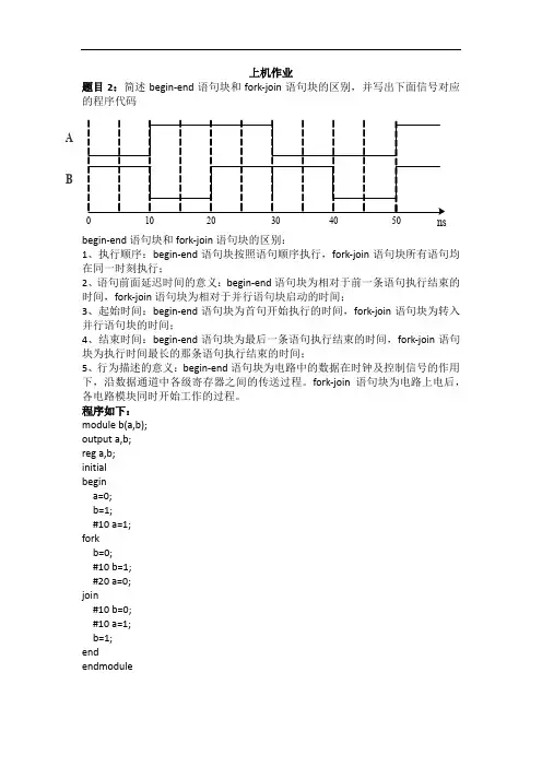
上机作业题目2:简述begin-end 语句块和fork-join 语句块的区别,并写出下面信号对应的程序代码begin-end 语句块和fork-join 语句块的区别:1、执行顺序:begin-end 语句块按照语句顺序执行,fork-join 语句块所有语句均在同一时刻执行;2、语句前面延迟时间的意义:begin-end 语句块为相对于前一条语句执行结束的时间,fork-join 语句块为相对于并行语句块启动的时间;3、起始时间:begin-end 语句块为首句开始执行的时间,fork-join 语句块为转入并行语句块的时间;4、结束时间:begin-end 语句块为最后一条语句执行结束的时间,fork-join 语句块为执行时间最长的那条语句执行结束的时间;5、行为描述的意义:begin-end 语句块为电路中的数据在时钟及控制信号的作用下,沿数据通道中各级寄存器之间的传送过程。
fork-join 语句块为电路上电后,各电路模块同时开始工作的过程。
程序如下: module b(a,b); output a,b; reg a,b; initial begin a=0; b=1; #10 a=1; fork b=0; #10 b=1; #20 a=0; join#10 b=0; #10 a=1; b=1; endendmoduleA B题目3.分别用阻塞和非阻塞赋值语句描述如下图所示移位寄存器的电路图。
D Q D Q dinclk D Q D Qout3out2out1out0程序如下:module block1(din,clk,out0,out1,out2,out3); input din,clk;output out0,out1,out2,out3;reg out0,out1,out2,out3;always@(posedge clk)beginout3=out2;out2=out1;out1=out0;out0=din;endendmodulemodule non_block1(din,clk,out0,out1,out2,out3); input din,clk;output out0,out1,out2,out3;reg out0,out1,out2,out3;always@(posedge clk)beginout0<=din;out1<=out0;out2<=out1;out3<=out2;endendmodule题目4:设计16位同步计数器要求:(1)分析16位同步计数器结构和电路特点;(2)用硬件描述语言进行设计;(3)编写测试仿真并进行仿真。
《数字集成电路》上机实验姓名:***班级:***学号:***第一次实验一、实验目的:掌握HSPICES软件的使用方法,用于分析二极管及CMOS反相器的直流特性,通过改变电源电压及MOS管的宽长比得到一组CMOS反相器的电压传输特性曲线,从而理解CMOS反相器电压传输特性曲线的影响因素和调整方法。
二、实验内容:1. 由上图所示,令(1)I S=10-14A,T=300K;(2) I S=10-16A,T=300K;(3) I S=10-14A,T=350K,利用SPICE求解V D1、V D2和I D。
【仿真代码】.TITLE amplifierSHU.LIB 'D:\Digital\lib\csmc06.LIB' TT.TEMP temvalueR1 1 2 2kR2 3 4 2kD1 2 3 DMODD2 4 0 DMOD.MODEL DMOD D Is=isvalue.PARAM temvalue=27 isvalue=1E-14 V1 1 0 DC 2.5.OP.ALTER.PARAM temvalue=27 isvalue=1E-16 .ALTER.PARAM temvalue=77 isvalue=1E-14 .OPIONS LIST NODE POST=2.END【结果】【分析】V D1=525.4463mv、V D2=525.4463mv和I D=362.2768uA2. (1)由下图所示,令Vin从0V变化到2.5V,步长为0.5V,利用SPICE求M1管电流变化的曲线,判断管子的工作状态;当M1的尺寸变化为W/L=4u/1u时,求I M1,并解释两条曲线存在误差的原因。
【仿真代码】.TITLE amplifierSHU.LIB 'D:\Digital\lib\mix025_1.lib' TT.PARAM dd=2.5Vdd 1 0 DC ddVin 2 0 DCM_M1 0 2 1 1 pch L=1U W=4U.DC Vin 0 2.5 0.5.PRINT I(2).OP.OPTION NODE LIST POST.END.TITLE amplifierSHU.LIB 'D:\Digital\lib\mix025_1.lib' TT.PARAM dd=2.5Vdd 1 0 DC ddVin 2 0 DCM_M1 0 2 1 1 pch L=0.25U W=1U .DC Vin 0 2.5 0.5.PRINT I(2).OP.OPTION NODE LIST POST.END【结果】【分析】在1.5V之前是工作在线性区,1.5-2V之间是可变电阻区,2V以后工作在饱和区。
《Verilog HDL硬件描述语言》实验教学大纲
课程代码:MICR3001
课程名称:Verilog HDL硬件描述语言
英文名称:Verilog HDL
实验室名称:微电子实验室
课程学时:72实验学时:18
一、本课程实验教学目的与要求
通过实验要求学生掌握用Verilog HDL硬件描述语言进行集成电路设计的流程和方法。
学会使用Max+plusⅡ,QuartusⅡ设计软件,掌握从HDL源代码的输入→编译→仿真→管脚锁定→下载全过程。
学会用ModelSim设计软件,用Verilog HDL编写测试码对设计模块进行仿真。
二、主要仪器设备及现有台套数
PC,现有35台; EDA实验箱,25套;
1、实验报告:有设计代码,仿真结果,管脚排列,验证结果。
2、考核方式:
(1)实验课的考核方式:教师验收评定成绩。
(2)实验课考核成绩:根据实验完成情况和实验报告是否完整确定,实验课成绩占课程总成绩的10%。
五、实验教材、参考书
1、教材:在编
2、参考书:J.Bhasker著,夏宇闻等译《Verilog HDL入门》.北京航空航天大学出版社.2008出版。

基于V e r i l o g H D L的自动售货机设计Pleasure Group Office【T985AB-B866SYT-B182C-BS682T-STT18】密级:NANCHANG UNIVERSITY学士学位论文THESIS OF BACHELOR(2012 —2016年)题目基于Verilog HDL的自动售货机设计学院:信息工程学院系电子信息工程系专业班级:学生姓名:学号:指导教师:职称:教授起讫日期:基于Verilog HDL的自动售货机设计学生姓名:田启泽指导教师:陶凌摘要自动售货机是商业自动化的常用设备,它不受地点和时间的限制,能够支持线上,线下多种支付方式,出货迅速,并且操作简单方便,因此受到了社会各群体的欢迎。
现目前自动售货机多为单片机设计,常出现因功能单一不能满足顾客需求,性能不稳定带来各种售货出错等现象。
本文将论述采用EDA方法,以QuartusⅡ为软件开发平台,使用Verilog HDL 语言设计,经过仿真后,在FPGA器件中实现自动售货机系统的详细流程。
经过仿真验证设计可以实现投币计次,两种售价均为两元的商品选择,购物操作无条件取消,按键消抖,以及投币退币数量显示功能。
硬件电路用一个按键电路实现投币功能,以led的点亮的数量指示投币的数量和商品出货情况,并以七段数码管显示退币的数量。
关键词:自动售货机;Verilog HDL;FPGA;EDA;Quartus ⅡDesign of Vending Machine Based on VHDLAbstractVending machines are commonly used as commercial automated equipment, it is not restricted some trouble aspects,such as place,time and so on. It support online, offline payment methods, fast shipping, and easy operation, therefore has been welcomed by all social groups. Vending machines are currently a mostly single-chip design, often due to a single function can not meet customer needs, bring a variety of sales performance problems due to unstable capability.This article will discusses the selling process of the vending machine by using QuartusⅡas software development platform, with the EDA method and through Verilog HDL language designing, after simulating, complying vending machine system in FPGA devices. After simulation designed it can be achieved coin metering and selection of commodities both are priced at two yuan, unconditionally canceled, key debounce and coin-coin number display. Hardware circuit using a function key circuits replays coin-operated,the number of led lights indicates the number of shipments of goods and coin, and using seven-segment LED to display the number of coin return.Keywords: vending machine;Verilog HDL;FPGA;EDA;Quartus Ⅱ目录14683 4 5 6第一章绪论自动售货机研究背景中国产业调研网发布的2016年版中国自动售货机市场现状调研与发展趋势趋势分析报告认为,居民收入水平显步攀升,自动售货机的迅猛发展得益于消费群体追逐灵活、智能、高效以及自助式服务。
verilog hdl 习题答案Verilog HDL 习题答案Verilog HDL(硬件描述语言)是一种用于描述数字电路的硬件描述语言,它被广泛应用于数字系统的设计和验证。
在学习Verilog HDL的过程中,练习题是非常重要的,通过解答习题可以加深对Verilog HDL语言的理解,并提高设计和编程的能力。
下面我们将为您提供一些Verilog HDL习题的答案,希望能够帮助您更好地掌握这门语言。
1. 请编写一个Verilog HDL模块,实现一个4位全加器。
module full_adder(input wire a, b, cin,output wire sum, cout);assign sum = a ^ b ^ cin;assign cout = (a & b) | (b & cin) | (a & cin);endmodule2. 请编写一个Verilog HDL模块,实现一个4位加法器。
module adder_4bit(input wire [3:0] a, b,output wire [3:0] sum);wire c0, c1, c2;full_adder fa0(a[0], b[0], 1'b0, sum[0], c0);full_adder fa1(a[1], b[1], c0, sum[1], c1);full_adder fa2(a[2], b[2], c1, sum[2], c2);full_adder fa3(a[3], b[3], c2, sum[3], );endmodule3. 请编写一个Verilog HDL模块,实现一个4位移位寄存器。
module shift_register(input wire clk, rst, shift,input wire [3:0] in,output wire [3:0] out);reg [3:0] reg_data;always @(posedge clk or posedge rst) beginif(rst)reg_data <= 4'b0;else if(shift)reg_data <= {reg_data[2:0], in[0]};elsereg_data <= in;endassign out = reg_data;endmodule以上是一些常见的Verilog HDL习题的答案,通过这些习题的练习,相信您对Verilog HDL语言的掌握会更加深入。
2013届本科生毕业设计题目:基于STC89C52单片机的数控直流恒流源设计作者姓名:蔡付平学号: 2009080347系 (院): 机械与电子工程学院专业:电子信息工程指导教师姓名: 邵毅指导教师职称:讲师2012年11月15日SuZhou UniversityYear 2013Bachelor Graduationl ssignmentTitle:Based on the 51 microcontroller numerical DC power supplydesignAuthor: Cai FupingStudent ID: 2009080347Department: College of mechianical and Electronical Engineering Major: Electrical Information EngineeringInstructotr: Shao YiProfessional Title: LecturerNov ember 15, 2012摘要该数控直流恒流源基于STC89C52单片机为核心控制器,采用模块化设计, 提高了恒流源的输出精度和稳定度。
本系统由单片机程序控制设定电流值,经过D/A转换器(TLC5618)输出模拟量,再经过运算放大器隔离放大,控制输出功率管的栅极,随着功率管栅极电压的变化而输出不同的电流。
同时单片机系统还兼顾对恒流源进行实时监控,输出电流经过电流/电压转换后,再通过A/D转换芯片(TLC2543),实时把模拟量转化为数据量,提供给单片机进行数据处理,通过数字量形式的闭环反馈环节,使电流更加稳定,这样便构成稳定的压控电流源。
由于系统采用负反馈闭环控制系统进行稳流,可最终实现精度高、稳定性好、输出范围宽的要求。
该数控电流源实现输出电流范围0~2000mA范围内任意设定(0~10Ω负载下);输出电流调整采用步进式(Step:±1mA)输出电流调整率≤2%(0~10Ω负载下);按键显示控制输出电流大小;断电后可以保持最后一次设定电流值;而且还有过压报警、温度检测保护模块。
实验报告课程名称:HDL及系统设计授课班级:学号:姓名:指导老师:目录目录 (2)实验一Modelsim 仿真软件的使用 (3)实验二简单组合电路设计 (8)实验三二进制全加器设计 (10)实验四二进制计数器设计 (12)参考文献 (15)实验一Modelsim 仿真软件的使用一、实验目的(1)熟悉Modelsim 软件;(2)掌握Modelsim 软件的编译、仿真方法(3)熟练运用Modelsim 软件进行HDL 程序设计开发二、实验步骤附1、建立工程运行Modelsim软件,选择菜单File > New >Project,设置工程相关信息,如图1.1所示。
图1.1 modelsim新建工程附2、添加文件到工程点击ok,产生图1.2,添加文件到工程。
图1.2 添加文件到工程如果测试文件testio.v和t_testio.v没有事先编写,则选择Create New File,并输入以下程序:module testio(key1,led1);input key1;output led1;assign led1 = ~ key1;endmodulemodule t_testio;reg data_in;wire data_out;initialbegindata_in = 0;#50 data_in = 1;#50 data_in = 0;#50 data_in = 0;$stop;endtestio test(.key1(data_in),.led1(data_out));endmodule注:两个程序两个文件附3、编译文件选择菜单 Compile > Compile All附4、查看编译后的设计单元如图1.3所示,双击t_testio。
得到编译环境图1.4。
图1.3 库文件显示图图1.4 编译环境图附5、将信号加入波形窗口a 右键点击t_testiob 选择菜单Add > Add to Wave附6、运行仿真在VSIM >下输入run 500二、实验结果三、实验内容用 Verilog HDL 程序实现一个异或门,Modelsim 仿真,观察效果。
《Verilog HDL 数字集成电路设计原理与应用》上机作业班级:******* 学号:******* 姓名:*******题目1:数字集成电路的verilog HDL 描述与仿真。
要求:(1)学习使用Modelsim 设计和仿真软件; (2)练习教材7.2.1中的例子;(3)掌握设计代码和测试代码的编写; (4)掌握测试仿真流程;(5)掌握Modelsim 软件的波形验证方式。
解答:题目2: 简述begin-end 语句块和fork-join 语句块的区别,并写出下面信号对应的程序代码A B解答:(1)begin-end语句块和fork-join语句块的区别:1、执行顺序:begin-end语句块按照语句顺序执行,fork-join语句块所有语句均在同一时刻执行;2、语句前面延迟时间的意义:begin-end语句块为相对于前一条语句执行结束的时间,fork-join语句块为相对于并行语句块启动的时间;3、起始时间:begin-end语句块为首句开始执行的时间,fork-join语句块为转入并行语句块的时间;4、结束时间:begin-end语句块为最后一条语句执行结束的时间,fork-join语句块为执行时间最长的那条语句执行结束的时间;5、行为描述的意义:begin-end语句块为电路中的数据在时钟及控制信号的作用下,沿数据通道中各级寄存器之间的传送过程。
fork-join语句块为电路上电后,各电路模块同时开始工作的过程。
(2)程序代码:Begin-end语句:module initial_tb1;reg A,B;initialbeginA=0;B=1;#10 A=1;B=0;#10 B=1;#10 A=0;#10 B=0;#10 A=1;B=1;endendmoduleFrk-join语句:module wave_tb2;reg A,B;parameter T=10;initialforkA=0;B=1;#T A=1;B=0;#(2*T) B=1;#(3*T) A=0;#(4*T) B=0;#(5*T) A=1;B=1;joinendmodule题目3. 分别用阻塞和非阻塞赋值语句描述如下图所示移位寄存器的电路图。
解答:(1)阻塞赋值语句module block2(din,clk,out0,out1,out2,out3);input din,clk;output out0,out1,out2,out3;reg out0,out1,out2,out3;always@(posedge clk)beginout0=din;out1=out0;out2=out1;out3=out2;endendmodule(2)非阻塞赋值语句module non_block1 (din,clk,out0,out1,out2,out3);input din,clk;output out0,out1,out2,out3;reg out0,out1,out2,out3;always@(posedge clk)beginout0<=din;out1<=out0;out2<=out1;out3<=out2;endendmodule题目4:设计16位同步计数器要求:(1)分析16位同步计数器结构和电路特点;(2)用硬件描述语言进行设计;(3)编写测试仿真并进行仿真。
解答:(1)电路特点:同步计数器的时间信号是同步的;每当到达最高计数后就会重新计数。
(2)程序代码:module comp_16 (count, clk, rst );output [15:0] count;input clk,rst;reg [15:0] count;always @ (posedge clk)if (rst)count<=16'b0000000000000000;elseif (count==16'b1111111111111111)count<=16'b0000000000000000;elsecount<=count+1;endmodule(3)仿真代码:module comp_16_tb;wire [15:0] count;reg clk,rst;comp_16 U1 (count, clk, rst );always #1 clk=~clk;initialbeginclk=0;rst=0;#1 rst=1;#10 rst=0;#10 rst=1;#10 rst=0;#99999 $finish;endendmodule题目5. 试用Verilog HDL门级描述方式描述如下图所示的电路。
解答:module zy(D0,D1,D2,D3,S1,S2,T0,T1,T2,T3,Z); output Z;input D0,D1,D2,D3,S1,S2; wire T0,T1,T2,T3,wire1,wire2; not U1(wire1,S1), U2(wire2,S2);and U3(T0,D0,wire2,wire1), U4(T1,D1,S1,wire1), U5(T2,D2,S1,wire2), U6(T3,D3,S1,S2); or U7(Z,T0,T1,T2,T3,); endmodule题目6. 试用查找真值表的方式实现真值表中的加法器,写出Verilog HDL 代码:Z解答:module homework6(SUM,COUT,A,B,CIN);output SUM,COUT;input A,B,CIN;reg SUM,COUT;always@(A or B or CIN)case({A,B,CIN})3'b000:SUM<=0;3'b000:COUT<=0;3'b001:SUM<=1;3'b001:COUT<=0;3'b010:SUM<=1;3'b010:COUT<=0;3'b011:SUM<=0;3'b011:COUT<=1;3'b100:SUM<=1;3'b100:COUT<=0;3'b101:SUM<=0;3'b101:COUT<=1;3'b110:SUM<=0;3'b110:COUT<=1;3'b111:SUM<=1;3'b111: COUT<=1;endcaseendmodule题目7:设计16位同步加法器和乘法器要求:(1)分析16位同步加法器和乘法器结构和电路特点;(2)用硬件描述语言进行设计;(3)编写测试仿真并进行仿真。
解答:(1)16位同步加法器和乘法器结构和电路特点:加法器的进位只用考虑一位,但是乘法器的进位要考虑到32位才行。
(2)程序代码:16位同步加法器:module adder(a,b,c,sum,cout);output [15:0]sum;output cout;input [15:0]a,b;input c;assign {cout,sum}=a+b+c;endmodule16位同步乘法器:module multiplier(a,b,mul);input [15:0]a,b;output [31:0]mul;assign mul=a*b;endmodule(3)仿真代码:16位同步加法器:module adder_tb;reg [15:0]a,b;reg c;wire [15:0]sum;wire cout;initialbegina=8;b=8;c=1;endinitialbegin#10 a=16'b1111111111111111;#10 b=1;endadder U2(.a (a),.b (b),.c(c),.cout(cout),.sum(sum));endmodule16位同步乘法器:module multiplier_tb;reg [15:0]a,b;wire [31:0]mul;initialbegina=3;b=8;endinitialbegin#10 a=100;#15 b=100;endmultiplier U1(.a(a),.b(b),.mul(mul));endmodule仿真截图:加法器:乘法器:题目8. 将下面的状态转移图用Verilog HDL描述。
在图中,状态机的输入只与状态的跳转有关,与状态机的输出无关,因此该状态机为摩尔型状态机。
下面为三段式描述方式。
解答:程序代码:module homework8(clk,out,step,clr);output [2:0]out;input step,clk,clr;reg [2:0]out;reg [1:0]state,next_state;always @(posedge clk)state<=next_state;always @(state or clr)if(clr)next_state<=0;elsecase(state)2'b00:case(step)1'b0:begin next_state<=2'b00;out<=3'b001;end1'b1:begin next_state<=2'b01;out<=3'b001;endendcase2'b01:beginout<=3'b010;next_state<=2'b10;end2'b10:case(step)1'b0:begin next_state<=2'b00;out<=3'b100;end1'b1:begin next_state<=2'b11;out<=3'b100;endendcase2'b11:case(step)1'b0:begin next_state<=2'b11;out<=3'b111;end1'b1:begin next_state<=2'b00;out<=3'b111;endendcaseendcaseendmodule仿真代码:module homework8_tb;reg clk,step,clr;wire [3:0]out;always#5 clk=~clk;initialbegin clk=0;clr=1;step=1;endinitialbegin#5clr=0;#10 step=0;#10step=1;endhomework8 U1(clk,out,step,clr);endmodule仿真截图:题目9. 如下图所示电路,若其延迟时间设定如表所示,试写Verilog HDL程序设计该电路。