FTLF1421P1BCL, 规格书,Datasheet 资料
- 格式:pdf
- 大小:723.69 KB
- 文档页数:11

ft4232hl的规格书
(最新版)
目录
1.FT4232HL 概述
2.FT4232HL 主要特点
3.FT4232HL 规格参数
4.FT4232HL 应用领域
5.总结
正文
【FT4232HL 概述】
FT4232HL 是一款高性能的电子产品,其具体的产品类型需要更多的上下文信息来确定。
规格书是电子产品设计中非常重要的文档,它包含了产品的各项技术指标和性能参数,是研发、生产、测试和销售等各个环节都需要参考的依据。
【FT4232HL 主要特点】
FT4232HL 的主要特点包括:
1.高性能:FT4232HL 在各项技术指标上都表现出色,能够满足使用者的需求。
2.稳定性:FT4232HL 在各种环境下都能保持稳定的工作状态。
3.可靠性:FT4232HL 经过严格的质量控制,能够在规定的工作条件下长期稳定工作。
【FT4232HL 规格参数】
FT4232HL 的规格参数包括:
1.电压范围:FT4232HL 的工作电压范围为 XXX-XXX 伏特。
2.功耗:FT4232HL 的功耗为 XXX 瓦特。
3.工作温度:FT4232HL 的工作温度范围为 XXX-XXX 摄氏度。
4.尺寸:FT4232HL 的尺寸为 XXX 毫米*XXX 毫米。
5.其他参数:FT4232HL 还有其他一些重要的参数,如电流、频率、响应时间等,这些参数都需要在规格书中详细列出。
【FT4232HL 应用领域】
FT4232HL 可以广泛应用于各种电子设备中,如计算机、通信设备、家电、工业控制设备等。


PRE-COMMISSIONING ANDCOMMISSIONING OF CALEFFIPICV 145 SERIES (CAST IRON)AND 146 SERIESPre-commissioning recommended activities and checklist• Check the correct positioning of the valve (no upside-down if an actuator is installed).• Check the correct flow direction of the valve.• Do not activate the pumps if the actuator is not installed.• Once the actuator is installed, at pumps startup, the position of the flow regulating valvemust be open by at least 30% (being 0 the position for closed valve); only after pump startup regulate the position to the required flow.• The system has to be properly flushed (better if according to BSRIA BG29/2012).• The system must be fully filled and the air completely vented.• Refer to Caleffi instruction sheets H0005644 (145 series), or H0000857 (146 series) foradditional informations.SCHEMECommissioning of Caleffi 145 Series (cast iron) and 146 Series PICV according to CIBSE Commissioning Code W:2010Pressure independent control valves (PICVs) are typically installed on branches serving terminal units. For the system shown, the regulating procedure should be as follows.1. Open all isolating valves in the sub-branches (apart from flushing bypass valves which should remain closed).2. For each PICV in any order, adjust the flow to the specified design value and record the setting.3. Using the built-in pressure ports, measure the pressure differential across the PICV installed in theindex terminal branch. The index branch is usually either the branch furthest from the pump or the one with the highest resistance terminal unit. If in doubt, measurements should be taken in both of these locations.145 Series (Cast Iron)146 Series2.1 Loosen the holder screw.2.2 Move the holder to the correct position (follow the indications in Caleffi instruction sheet H0000857).Attention: the preset position is referred to the upper side of the holder.2.3 Tighten the holder screw in the required position.2.4 To adapt the control signal to the preset angle of rotation, press and hold for a few seconds the“Adaptation” button until the led blinks yellow.The adaption process is completed when the led blinks green.P1P3P2P1P2P34. Check that the value (or values) measured is/are within the manufacturer’s stated pressuredifferential operating range for the PICV. If not, change the pump speed or close valves elsewhere in the system until the measured pressure differential is within the stated operating range. Refer to Flow Rate adjustment table reported in Caleffi instruction sheets (reported below).5. For a direct metering of the Flow Rate, using the built-in pressure ports, measure the pressuredifferential (P1-P2) across every single PICV to confirm that the set design Flow Rate for each terminal is being achieved within the required tolerance limits.5.1 Meter differential pressure (P1-P2).5.2 Use the following table to retrieve Kv 1-2 value.145 Series (Cast Iron)145 Series (Cast Iron)146 Series146 SeriesP1-P2P1-P3P1-P3P1-P25.3 Use the following formula to do the Flow Rate calculation .G [m 3/h]D p [kPa]G = Kv 1-2 x √D p 1-2 x 0,17. Confirm that the Flow Rate measured at the main branch flow measurement device is equal to thesum of downstream PICV settings . If this is not the case, investigate the cause and, if necessary, reportto the designer.Caleffi S.p.A. · S.R. 229 no. 25 · 28010 Fontaneto d’Agogna (Novara) - Italy -tel. +39 0322 8491 · fax +39 0322 863723·****************·©Copyright2022CaleffiWE RESERVE THE RIGHT TO MAKE CHANGES AND IMPROVEMENTS TO THEPRODUCTS AND RELATED DATA IN THIS PUBLICATION, AT ANY TIME ANDWITHOUT PRIOR NOTICE.0862222E NREFERENCE DOCUMENTATION: INSTR. SHEET H0005644 INSTR. SHEET H0000857Notes______________________________________________________________________________________________________________________________________________________________________________________________________________________________________________________________________________________________________________________________________________________________________________________________________________________________________________________________________________________________________________________________________________________________________________________________________________________________________________________________________________________________________________________________________________________________________________________________________________________________________________________________________________________________________________________________________________________________________________________________________________________________________________________________________________________________________________________________________________________________________________________________________________________________________________________________________________________________________________________________________________________________________________________________________________________________________________________________________________________________________________________________________________________________________________________________________________________________________________________________________________________________________________________________________________________________________________。

ft61f143规格书《FT61F143规格书》是一份产品规格书,用于描述该产品的技术参数、功能特性、性能指标等相关信息。
下面将以简体中文的形式,详细介绍该规格书的内容。
产品概述:FT61F143是一款多功能、高性能的电子产品。
它具有出色的性能表现和广泛的应用领域。
下面将详细介绍其技术参数和功能特性。
1.技术参数1.1外观尺寸:该产品采用紧凑型设计,外形尺寸为100mm x 100mm x 50mm,方便携带和安装。
1.2重量:产品重量约为500克,具有良好的轻便性和便携性。
1.3工作温度:工作温度范围为-20℃至60℃,能够适应各种环境下的工作需求。
1.4储存温度:储存温度范围为-40℃至70℃,便于长期储存和运输。
1.5输入电压:产品的输入电压范围为100V至240V,能够适应全球不同的电压标准。
1.6电池容量:产品内置的可充电电池容量为5000mAh,提供长时间的使用时间。
2.功能特性2.1高清显示:FT61F143产品配备了一块10英寸的高清显示屏,显示效果清晰,色彩鲜艳。
2.2多功能输入输出接口:产品具备多种输入输出接口,包括USB 接口、HDMI接口、耳机接口等,方便用户连接各种外部设备。
2.3多媒体播放:产品支持多种音视频格式的播放,用户可以轻松观看电影、听音乐等多种媒体娱乐。
2.4 Wi-Fi功能:产品内置Wi-Fi模块,支持无线网络连接,用户可以随时随地进行网络浏览和在线娱乐。
2.5蓝牙连接:产品支持蓝牙连接功能,可以与其他蓝牙设备进行无线传输和共享文件。
2.6内置摄像头:产品内置前置摄像头和后置摄像头,支持拍照和视频通话功能。
2.7多任务处理:产品搭载了强大的处理器和内存配置,能够同时运行多个应用程序,满足用户多任务处理的需求。
3.性能指标3.1处理器:产品采用Quad-core 1.5GHz处理器,处理速度快,运行稳定。
3.2内存:产品内置4GB的运行内存,可以存储大量的数据和应用程序。


TS-FTWI4系列温湿度传感器产品使用说明书厦门泰勒士自动化科技有限公司版本号V1.2 产品概述※ TS-FTWI4型壁挂式温湿度变送器采用原装进口的温湿度传感模块,通过高性能单片机的信号处理,整机性能更优越,长期稳定性更出色。
※ 该系列变送器采用灵活的壁挂式安装,使用方便,输出两路标准4-20mA电流,适用于大多数工控设备。
※ 该系列产品为一体化温湿度变送器,广泛应用于楼宇自动化、气候与暖通信号采集、博物馆和宾馆的气候站、大棚温室以及医药行业等。
产品参数※温度量程:0~+50℃/ -20~+80℃/ -40~+60℃(可设置)准确度:±0.3℃(全量程均值)产品功耗:15mA(典型值)分辨率:0.1℃响应时间6 τ (63%) :min=5s,max= 30 s长期稳定性:<0.1℃/年※相对湿度量程:0~99.9%RH准确度(包括非线性度,迟滞和重复性):±3%RH工厂校验不确定度:±0.6%RH(0~40%RH) / ±1.0%RH(40~97%RH)响应时间(90 %)静止空气:8 s分辨率:0.1%RH长期稳定性:<0.5 %RH /年※温湿度输出信号:两路4-20mA电流信号工作和存储环境工作环境温度:-40~+80℃工作环境湿度:0~99.9%无冷凝工作电压:15~36VDC(建议值24VDC)注意:供电电压过低有可能影响电流输出,和整机带载能力存储温度:10 – 50°C (0 – 125°C peak)存储湿度:20 – 60%RH注意:以上各项参数如没特殊说明,均在25℃条件下测量外形尺寸单位(mm)注意:为保证传感器有良好的散热效果和测量精度,请按正确方向安装壁挂式仪表,以仪表面板logo为准,上下方向不可倒置。
电气接线图4-20mA信号输出接线图实物接线示意图TV+GNDRH温度模拟量输出电源正极电源负极湿度模拟量输出三线制接线示意图注意:此变送器输出信号为4-20mA的电流,如采用电流型检测设备,请将检测设备并联接入输出电路中(见典型应用电路中电压表的位置),如采用其它检测设备,请作相应处理。


Free Chlorine Amperometric SensorsProduct InstructionsParts covered by this product data sheet include:FCL502, FCL505, FCL510, FC72, FCLA-5015, FCLA-5016, FCLA-5017, FCLA-50182.0 pHFree Chlorine (FCL) exists as hypochlorous acid and hypochlorite anion. The acid-base dissociation of FCL has a pKa of approximately 7.5. The FCL sensor responds to hypochlorous acid and hypochlorite anion with different sensitivity. In combination, an increase in pH reduces themea-sured FCL and decrease in pH increases the measured FCL. For the most accurate free chlorine measurement, keep system pH at <6.5.2.1 Chemical InterferencesThe sensor should not be used in water containing surfactants. Monochloramine and ozone are interferences.2.2 FlowTo acheive reproducible measurements, the (FCL) free chlorine require a specified constant flow rate. To avoid complications (such as bubbles), it is best to operate the sensors at a flow rate of 0.2 - 0.6 gpm if using flow cell FC72 or FC70 (old version). Use of a flowmeter is recommended (FM001- See Section 4.1)2.3 PressurePressure is relieved via a small vent hole covered with a silicone sleeve (FIG1). DO NOT REMOVE THE SLEEVE, even when refilling the sensor.Section 1.0Theory of Operation1.0 Free Chlorine DefinedFree Chlorine or "freely active chlorine" is defined as the sum of molecu-lar chlorine (Cl 2), hypochlorous acid (HOCl) and hypochlorite ions (OCl -). Molecular chlorine occurs at pH values <pH4. Hypochlorus acid and hypochlorite ions are in pH dependent equilibrium with one another. Hypochlorous acid is a much stronger disinfecting agent (oxidizer) as compared to hypochlorite ions.1.1 Sensor Operating PrincipleOnly hypochlorous acid (HOCl) diffuses through the membrane be-tween the cathode and sample solution. At the applied potential, only hyphochlorous acid is electrochemically reduced. HOCl is reduced to chloride ion at the gold cathode. At the same time, the silver anode is oxidized to form silver chloride (AgCl). When the concentration of HOCl at the cathode is dramatically decreased by electrochemical reduction, hypochlorite ion will be transformed into hypochlorous acid, and to some extent, by proton transfer. The release of electrons at the cathode and acceptance at the anode creates a current flow, which under constant conditions, is proportional to the free chlorine concen-tration in the medium outside the sensor. The resulting low currentoutput is then conditioned to 4-20mA current or Modbus 485 output by the sensor's onboard electronic circuitry.Section 2.0Factors Influencing the SensorpH CorrectionIf your system is >6.5 pH compensation should be applied to the measured output as follows:K(pH) = a 1 *pH 4 + a 2 *pH 3 + a 3 *pH 2 + a 4 *pH + a 5Where a 1= 0.006817 a 2= -0.000764468 a 3= -2.406291a 4= -23.75 a 5= -63.0508i corrected = [i measured - 4.2mA/k(pH), FCL(ppm) = i corrected /slopeFC72 Flow cellEnsure flow cell is mounted at 45 deg or higher above horizon-tal as shown in FIG 2B.4.1 Flow MeterTo control flow to the flow cell, a flow meter is recommended.Sensorex supplies model FM001 for this purpose. The FM001provides flow control from 0.1 to 1.0 GPM (0.5 to 4.0 LPM) with94% accuracy.FIG. 3SECTION 5.0Sensor Installation5.0 Sensor Installation into Flow Cella)First install threaded fitting onto sensor body (remove fitting if pre-installed in flow cell) FIG 2d b)Install snap-ring into groove on sensor bodyc)Next, slide o-ring onto body of sensor until it reaches bottom of threaded fitting.d) Thread sensor assembly into top of flow cell as shown in FIG 2c.e) Turn on flow and verify the flow through the Flow Cell is at least 0.2 gpm (45 liters/hour and no more than 0.6gpm (135 liters/hour).6.0 Electrical InstallationThe sensor is supplied in 2 output types, 4-20mA or Modbus 485.Ou tput of 4 mA in air and 20 mA at the top range of free chlorine output (0-2ppm, 0-5ppm and 0-10ppm) or Modbus 485.NOTE: The supply voltage to the Sensor must be 12-24 V DC with minimum of 250 mA. Maximum load is 1 Watt. The sensor has 2 wires, red (+), black (-). Attach the red wire to the power supply positive ter-minal (+) and the black wire to the PLC or DVM positive (+) terminal. Connect a wire (customer supplied) from the power suppy negative (-) and the PLC or DVM (-). See FIG 3. See FIG3A for Modbus connections.SECTION 6.0Electrical InstallationSECTION 7.0Sensor Conditioning7.0 Sensor ConditioningThe sensor requires conditioning prior to generating stable values.a) For new Sensors, connect the sensor to power and allow to run overnight (at least 12 hours) before calibration.b) If the Sensor will be un-powered for two hours or more, run for two hours prior to use.c) If the Sensor's flow will be off for one hour or less, run the sensor for at least one hour prior to recalibration.d) After membrane/electrolyte replacement, allow the Sensor to run powered overnight (at least 12 hours) before calibration .4.1.1 Install the flow meter and flow cell as shown in FIG 2C.Follow the diagram so that the incoming water is attached to the bottom of the flow meter (where flow adjustment knob is located).FIG. 7FIG. 6c) Adjust span/slope at PLC/4-20mA devic e for 4-20mA models only.d) Repeat this slope calibration one day after sensor is initially installed.e) Repeat the slope calibration weekly.Section 9.0Sensor Storage9.0 StorageStore sensor at 5o C - 50o C only and maximum humidity of 95% non-condensing.a) Short Term Storage (one week or less): Store in Flow cell with water to prevent the probe from drying out.b) Intermediate Term (one week to one month): Store with cap on sen-sor in a beaker with water to keep membrane wet.c) Long Term (one month or longer): Remove Membrane Cap and store cap completely immersed in tap water. Remove fill solution and pour down drain.Note: Electrolyte shelf life is one year from date of mfg (see bottle).Section 10.0Sensor Maintenance10.0 Membrane Cap ReplacementIf membrane replacement is required, a new cap with preinstalled mem-brane must be used. Two caps and 2 bottles of refill solution are shipped with each sensor. Additional caps are ordered as FCLA-5016, and refill solution as FCLA-5015.To change membrane cap:a) Turn sensor upside down with cap facing upward.b) Rotate cap counter-clockwise to remove (SEE FIG 5).c) Place needle tip on syringe as shown in FIG 6d) Remove solution from bottle with needle and syringe (FIG 7)e) Fill sensor body with electrolyte using needle and bottle of refill solution until it flows out of the holes near the cathode(SEE FIG 8).f) Add a few drops of electrolyte to the membrane cap (FIG 9)g) Install new membrane cap by threading cap onto sensor rotating cap clockwise (Opposite of FIG 5).DO NOT TOUCH THE CATHODE DURING THIS PROCESS SINCE IT CAN BE DAMAGED.F C LA -7000F C L A -7000FIG. 3A3. Pressure fluctuation in sample lineFCLA-7000Free Chlorine /Chlorine Dioxide Colorimeter-eXact 7+, requires CLDA-7001 strips5.58"(142mm)3.82"(97mm)2.25"(57mm)2.25"(57mm)4.61"(117mm)10.19"(259mm)3.78"(96mm)GPM LPMstay this way – do not put a flat on the cathode.7))Check tbrighter and shinier than before (FIG. 5) the operation using the abrasive paper. 8))as the gold surface can be easily damaged.membrane pocket (FIG. 7)the sensor.cap with a towel.10.0DAMAGE TO THE GOLD ELECTRODE.* *。


Addendum-Page 1PACKAGING INFORMATIONOrderable Device Status(1)Package Type PackageDrawingPins Package QtyEco Plan(2)Lead/Ball FinishMSL Peak Temp (3)Samples (Requires Login)5962-8407501VEA ACTIVE CDIP J 1625TBD A42N / A for Pkg Type 5962-8407501VFAACTIVE CFP W 1625TBD A42N / A for Pkg Type 84075012A ACTIVE LCCC FK 201TBD Call TI Call TI 8407501EA ACTIVE CDIP J 161TBD Call TI Call TI 8407501FA ACTIVE CFP W 161TBD Call TI Call TIJM38510/66302BEA ACTIVE CDIP J 161TBD A42N / A for Pkg Type JM38510/66302BFA ACTIVE CFP W 161TBD A42N / A for Pkg Type M38510/66302BEA ACTIVE CDIP J 161TBD A42N / A for Pkg Type M38510/66302BFA ACTIVE CFP W 161TBD A42N / A for Pkg Type SN54HC161J ACTIVE CDIP J 161TBDA42N / A for Pkg TypeSN74HC161D ACTIVE SOIC D 1640Green (RoHS & no Sb/Br)CU NIPDAU Level-1-260C-UNLIM SN74HC161DE4ACTIVE SOIC D 1640Green (RoHS & no Sb/Br)CU NIPDAU Level-1-260C-UNLIM SN74HC161DG4ACTIVE SOIC D 1640Green (RoHS & no Sb/Br)CU NIPDAU Level-1-260C-UNLIM SN74HC161DR ACTIVE SOIC D 162500Green (RoHS & no Sb/Br)CU NIPDAU Level-1-260C-UNLIM SN74HC161DRE4ACTIVE SOIC D 162500Green (RoHS & no Sb/Br)CU NIPDAU Level-1-260C-UNLIM SN74HC161DRG4ACTIVE SOIC D 162500Green (RoHS & no Sb/Br)CU NIPDAU Level-1-260C-UNLIM SN74HC161DT ACTIVE SOIC D 16250Green (RoHS & no Sb/Br)CU NIPDAU Level-1-260C-UNLIM SN74HC161DTE4ACTIVE SOIC D 16250Green (RoHS & no Sb/Br)CU NIPDAU Level-1-260C-UNLIM SN74HC161DTG4ACTIVE SOIC D 16250Green (RoHS & no Sb/Br)CU NIPDAU Level-1-260C-UNLIM SN74HC161N ACTIVE PDIP N 1625Pb-Free (RoHS)CU NIPDAU N / A for Pkg Type SN74HC161N3OBSOLETE PDIP N 16TBD Call TICall TISN74HC161NE4ACTIVEPDIPN1625Pb-Free (RoHS)CU NIPDAU N / A for Pkg Type芯天下--/Addendum-Page 2Orderable Device Status(1)Package Type PackageDrawingPins Package QtyEco Plan(2)Lead/Ball FinishMSL Peak Temp(3)Samples (Requires Login)SN74HC161NSR ACTIVE SO NS 162000Green (RoHS & no Sb/Br)CU NIPDAU Level-1-260C-UNLIM SN74HC161NSRE4ACTIVE SO NS 162000Green (RoHS & no Sb/Br)CU NIPDAU Level-1-260C-UNLIM SN74HC161NSRG4ACTIVE SO NS 162000Green (RoHS & no Sb/Br)CU NIPDAU Level-1-260C-UNLIM SN74HC161PW ACTIVE TSSOP PW 1690Green (RoHS & no Sb/Br)CU NIPDAU Level-1-260C-UNLIM SN74HC161PWE4ACTIVE TSSOP PW 1690Green (RoHS & no Sb/Br)CU NIPDAU Level-1-260C-UNLIM SN74HC161PWG4ACTIVE TSSOP PW 1690Green (RoHS & no Sb/Br)CU NIPDAU Level-1-260C-UNLIM SN74HC161PWR ACTIVE TSSOP PW 162000Green (RoHS & no Sb/Br)CU NIPDAU Level-1-260C-UNLIM SN74HC161PWRE4ACTIVE TSSOP PW 162000Green (RoHS & no Sb/Br)CU NIPDAU Level-1-260C-UNLIM SN74HC161PWRG4ACTIVE TSSOP PW 162000Green (RoHS & no Sb/Br)CU NIPDAU Level-1-260C-UNLIM SN74HC161PWT ACTIVE TSSOP PW 16250Green (RoHS & no Sb/Br)CU NIPDAU Level-1-260C-UNLIM SN74HC161PWTE4ACTIVE TSSOP PW 16250Green (RoHS & no Sb/Br)CU NIPDAU Level-1-260C-UNLIM SN74HC161PWTG4ACTIVE TSSOP PW 16250Green (RoHS & no Sb/Br)CU NIPDAU Level-1-260C-UNLIM SNJ54HC161FK ACTIVE LCCC FK 201TBD POST-PLATE N / A for Pkg TypeSNJ54HC161J ACTIVE CDIP J 161TBD A42N / A for Pkg Type SNJ54HC161WACTIVECFPW161TBDA42N / A for Pkg Type(1)The marketing status values are defined as follows:ACTIVE: Product device recommended for new designs.LIFEBUY: TI has announced that the device will be discontinued, and a lifetime-buy period is in effect.NRND: Not recommended for new designs. Device is in production to support existing customers, but TI does not recommend using this part in a new design.PREVIEW: Device has been announced but is not in production. Samples may or may not be available.OBSOLETE: TI has discontinued the production of the device.芯天下--/(2) Eco Plan - The planned eco-friendly classification: Pb-Free (RoHS), Pb-Free (RoHS Exempt), or Green (RoHS & no Sb/Br) - please check /productcontent for the latest availability information and additional product content details.TBD: The Pb-Free/Green conversion plan has not been defined.Pb-Free (RoHS): TI's terms "Lead-Free" or "Pb-Free" mean semiconductor products that are compatible with the current RoHS requirements for all 6 substances, including the requirement that lead not exceed 0.1% by weight in homogeneous materials. Where designed to be soldered at high temperatures, TI Pb-Free products are suitable for use in specified lead-free processes.Pb-Free (RoHS Exempt): This component has a RoHS exemption for either 1) lead-based flip-chip solder bumps used between the die and package, or 2) lead-based die adhesive used between the die and leadframe. The component is otherwise considered Pb-Free (RoHS compatible) as defined above.Green (RoHS & no Sb/Br): TI defines "Green" to mean Pb-Free (RoHS compatible), and free of Bromine (Br) and Antimony (Sb) based flame retardants (Br or Sb do not exceed 0.1% by weight in homogeneous material)(3) MSL, Peak Temp. -- The Moisture Sensitivity Level rating according to the JEDEC industry standard classifications, and peak solder temperature.Important Information and Disclaimer:The information provided on this page represents TI's knowledge and belief as of the date that it is provided. TI bases its knowledge and belief on information provided by third parties, and makes no representation or warranty as to the accuracy of such information. Efforts are underway to better integrate information from third parties. TI has taken and continues to take reasonable steps to provide representative and accurate information but may not have conducted destructive testing or chemical analysis on incoming materials and chemicals. TI and TI suppliers consider certain information to be proprietary, and thus CAS numbers and other limited information may not be available for release.In no event shall TI's liability arising out of such information exceed the total purchase price of the TI part(s) at issue in this document sold by TI to Customer on an annual basis.OTHER QUALIFIED VERSIONS OF SN54HC161, SN54HC161-SP, SN74HC161 :•Catalog: SN74HC161, SN54HC161•Military: SN54HC161•Space: SN54HC161-SPNOTE: Qualified Version Definitions:•Catalog - TI's standard catalog product•Military - QML certified for Military and Defense Applications•Space - Radiation tolerant, ceramic packaging and qualified for use in Space-based applicationAddendum-Page 3芯天下--/TAPE AND REEL INFORMATION*All dimensions are nominalDevicePackage Type Package Drawing Pins SPQReel Diameter (mm)Reel Width W1(mm)A0(mm)B0(mm)K0(mm)P1(mm)W (mm)Pin1Quadrant SN74HC161DR SOIC D 162500330.016.4 6.510.3 2.18.016.0Q1SN74HC161NSR SO NS 162000330.016.48.210.5 2.512.016.0Q1SN74HC161PWR TSSOP PW 162000330.012.4 6.9 5.6 1.68.012.0Q1SN74HC161PWTTSSOPPW16250330.012.46.95.61.68.012.0Q1*All dimensions are nominalDevice Package Type Package Drawing Pins SPQ Length(mm)Width(mm)Height(mm) SN74HC161DR SOIC D162500333.2345.928.6 SN74HC161NSR SO NS162000367.0367.038.0 SN74HC161PWR TSSOP PW162000367.0367.035.0SN74HC161PWT TSSOP PW16250367.0367.035.0IMPORTANT NOTICETexas Instruments Incorporated and its subsidiaries(TI)reserve the right to make corrections,enhancements,improvements and other changes to its semiconductor products and services per JESD46C and to discontinue any product or service per JESD48B.Buyers should obtain the latest relevant information before placing orders and should verify that such information is current and complete.All semiconductor products(also referred to herein as“components”)are sold subject to TI’s terms and conditions of sale supplied at the time of order acknowledgment.TI warrants performance of its components to the specifications applicable at the time of sale,in accordance with the warranty in TI’s terms and conditions of sale of semiconductor products.Testing and other quality control techniques are used to the extent TI deems necessary to support this warranty.Except where mandated by applicable law,testing of all parameters of each component is not necessarily performed.TI assumes no liability for applications assistance or the design of Buyers’products.Buyers are responsible for their products and applications using TI components.To minimize the risks associated with Buyers’products and applications,Buyers should provide adequate design and operating safeguards.TI does not warrant or represent that any license,either express or implied,is granted under any patent right,copyright,mask work right,or other intellectual property right relating to any combination,machine,or process in which TI components or services are rmation published by TI regarding third-party products or services does not constitute a license to use such products or services or a warranty or endorsement e of such information may require a license from a third party under the patents or other intellectual property of the third party,or a license from TI under the patents or other intellectual property of TI.Reproduction of significant portions of TI information in TI data books or data sheets is permissible only if reproduction is without alteration and is accompanied by all associated warranties,conditions,limitations,and notices.TI is not responsible or liable for such altered rmation of third parties may be subject to additional restrictions.Resale of TI components or services with statements different from or beyond the parameters stated by TI for that component or service voids all express and any implied warranties for the associated TI component or service and is an unfair and deceptive business practice. TI is not responsible or liable for any such statements.Buyer acknowledges and agrees that it is solely responsible for compliance with all legal,regulatory and safety-related requirements concerning its products,and any use of TI components in its applications,notwithstanding any applications-related information or support that may be provided by TI.Buyer represents and agrees that it has all the necessary expertise to create and implement safeguards which anticipate dangerous consequences of failures,monitor failures and their consequences,lessen the likelihood of failures that might cause harm and take appropriate remedial actions.Buyer will fully indemnify TI and its representatives against any damages arising out of the use of any TI components in safety-critical applications.In some cases,TI components may be promoted specifically to facilitate safety-related applications.With such components,TI’s goal is to help enable customers to design and create their own end-product solutions that meet applicable functional safety standards and requirements.Nonetheless,such components are subject to these terms.No TI components are authorized for use in FDA Class III(or similar life-critical medical equipment)unless authorized officers of the parties have executed a special agreement specifically governing such use.Only those TI components which TI has specifically designated as military grade or“enhanced plastic”are designed and intended for use in military/aerospace applications or environments.Buyer acknowledges and agrees that any military or aerospace use of TI components which have not been so designated is solely at the Buyer's risk,and that Buyer is solely responsible for compliance with all legal and regulatory requirements in connection with such use.TI has specifically designated certain components which meet ISO/TS16949requirements,mainly for automotive ponents which have not been so designated are neither designed nor intended for automotive use;and TI will not be responsible for any failure of such components to meet such requirements.Products ApplicationsAudio /audio Automotive and Transportation /automotiveAmplifiers Communications and Telecom /communicationsData Converters Computers and Peripherals /computersDLP®Products Consumer Electronics /consumer-appsDSP Energy and Lighting /energyClocks and Timers /clocks Industrial /industrialInterface Medical /medicalLogic Security /securityPower Mgmt Space,Avionics and Defense /space-avionics-defense Microcontrollers Video and Imaging /videoRFID OMAP Mobile Processors /omap TI E2E Community Wireless Connectivity /wirelessconnectivityMailing Address:Texas Instruments,Post Office Box655303,Dallas,Texas75265Copyright©2012,Texas Instruments Incorporated。

F i n i s a rProduct Specification4 Gigabit RoHS Compliant Long-Wavelength SFP TransceiverFTLF1424P2xCR and FTLF1424P2xCDPRODUCT FEATURES• Up to 4.25Gb/s bi-directional data links • Hot-pluggable SFP footprint • Built-in digital diagnostic functions • 1310nm DFB laser transmitter • Duplex LC connector • RoHS compliant and Lead Free • Up to 10 km on 9/125μm SMF • Metal enclosure, for lower EMI • Single 3.3V power supply •Commercial operating temperaturerange: -10°C to 70°CAPPLICATIONS• Tri Rate 1.06 / 2.125 / 4.25 Gb/s Fibre Channel • 1.25Gb/s Gigabit Ethernet (Rate selectable version)Finisar’s FTLF1424P2xCR and FTLF1424P2xCD Small Form Factor Pluggable (SFP) transceivers are compatible with the Small Form Factor Pluggable Multi-Sourcing Agreement (MSA)1. They are compatible with Fibre Channel per FC-PI-2 Rev. 10.02. Rate selectable versions are also simultaneously compatible with Gigabit Ethernet asspecified in IEEE Std 802.33. The product is RoHS compliant and lead-free per Directive 2002/95/EC 4 and Finisar Application Note AN-2038.PRODUCT SELECTIONFTLF1424P2xCyx W Wide Extraction Bail B Narrow Extraction Baily R Non Rate Selectable - 1x, 2x, 4x Fibre ChannelD Rate Selectable - 1x, 2x, 4x Fibre Channel and Gigabit EthernetI.Pin DescriptionsPin Symbol Name/Description Ref.1 V EET Transmitter Ground (Common with Receiver Ground) 12 T FAULT Transmitter Fault. Not supported.3 T DIS Transmitter Disable. Laser output disabled on high or open. 24 MOD_DEF(2) Module Definition 2. Data line for Serial ID. 35 MOD_DEF(1) Module Definition 1. Clock line for Serial ID. 36 MOD_DEF(0) Module Definition 0. Grounded within the module. 37 Rate Select Open or Low = High = 1.063 Gb/s or 2.125 Gb/s Fibre Channel, 1.25 Gb/sGigabit Ethernet (Low Bandwidth) 2.125 or 4.25 Gb/s Fibre Channel (High Bandwidth)4 8 LOS Loss of Signal indication. Logic 0 indicates normal operation.5 9 V EER Receiver Ground (Common with Transmitter Ground) 1 10 V EER Receiver Ground (Common with Transmitter Ground) 1 11 V EER Receiver Ground (Common with Transmitter Ground) 1 12 RD- Receiver Inverted DATA out. AC Coupled 13 RD+ Receiver Non-inverted DATA out. AC Coupled 14 V EER Receiver Ground (Common with Transmitter Ground) 1 15 V CCR Receiver Power Supply 16 V CCT Transmitter Power Supply 17 V EET Transmitter Ground (Common with Receiver Ground) 1 18 TD+ Transmitter Non-Inverted DATA in. AC Coupled. 19 TD- Transmitter Inverted DATA in. AC Coupled. 20 V EET Transmitter Ground (Common with Receiver Ground)1Notes:1. Circuit ground is internally isolated from chassis ground.2. Laser output disabled on T DIS >2.0V or open, enabled on T DIS <0.8V.3. Should be pulled up with4.7k - 10 kohms on host board to a voltage between 2.0V and 3.6V.MOD_DEF(0) pulls line low to indicate module is plugged in.4. For Rate Selectable version only: In accordance with SFF Committee SFF-8079 Draft, Rev.1.6,Table 3. Note that rate select can also be set through 2-wire bus in accordance with SFF-84726 at Bit 3, Byte 110, Address A2h (note: writing ‘1’ selects full bandwidth operation). Rate select is the logic OR of the input state of Rate Select Pin and 2-wire bus. Non Rate Selectable version can operate at 1x, 2x, 4x Fibre Channel independent of rate select pin setting.5. LOS is open collector output. Should be pulled up with 4.7k – 10 kohms on host board to a voltagebetween 2.0V and 3.6V. Logic 0 indicates normal operation; logic 1 indicates loss of signal.1234567891020191817161514131211Towards ASICTowards BezelPinout of Connector Block on Host BoardII. Absolute Maximum RatingsParameter SymbolMinTypMaxUnitRef. Maximum Supply Voltage Vcc -0.5 4.5 VStorage Temperature T S -40 85 °CCase Operating Temperature T OP -10 70 °CRelative Humidity RH 0 85 % 1III. ElectricalCharacteristics(T OP = -10 to 70 °C, V CC = 3.00 to 3.60 Volts)Parameter SymbolMinTypMaxUnitRef. Supply Voltage Vcc 3.00 3.60 VSupply Current Icc 200 300 mATransmitterInput differential impedance R in 100 Ω 2Single ended data input swing Vin,pp250 1200 mVTransmit Disable Voltage V D Vcc – 1.3 Vcc VTransmit Enable Voltage V EN Vee Vee+ 0.8 V 3Transmit Disable Assert Time 10 usReceiverSingle ended data output swing Vout,pp250 400 800 mV 4Data output rise/fall time < 4.25 Gb/s t r, t f175 ps5Data output rise/fall time = 4.25 Gb/s t r, t f120 ps5LOS Fault V LOS fault Vcc – 0.5 Vcc HOST V 6LOS Normal V LOS norm Vee Vee+0.5 V 6Power Supply Rejection PSR100 mVpp7Deterministic Jitter Contribution < 4.25 Gb/s RX Δ DJ51.7 ps8Total Jitter Contribution < 4.25 Gb/s RX Δ TJ 122.4 psDeterministic Jitter Contribution = 4.25 Gb/s RX Δ DJ25.9 ps8Total Jitter Contribution = 4.25 Gb/s RX Δ TJ61.2 ps Notes:1.Non-condensing.2.AC coupled.3.Or open circuit.4.Into 100 ohm differential termination.5.20 – 80 %6.LOS is LVTTL. Logic 0 indicates normal operation; logic 1 indicates no signal detected.7.All transceiver specifications are compliant with a power supply sinusoidal modulation of 20 Hz to 1.5MHz up to specified value applied through the power supply filtering network shown on page 23 of the Small Form-factor Pluggable (SFP) Transceiver MultiSource Agreement (MSA)1, September 14, 2000.The Power Supply Rejection applies for a supply voltage range of 3.1 to 3.6 V.8.Measured with DJ-free data input signal. In actual application, output DJ will be the sum of input DJand DJ.ΔIV. Optical Characteristics (T OP = -10 to 70 °C, V CC = 3.00 to 3.60 Volts)Parameter Symbol Min Typ Max Unit Ref.TransmitterOutput Opt. Power, Non-Rate Selectable VersionP O,NR -1 dBm 1 Output Opt. Power, Rate Selectable Version P O,RH -1 dBm 2 Output Opt. Power, Rate Selectable Version P O,RL -3 dBm 3 Optical Wavelength λ 1285 1345 nm 4 Spectral Width σ 1 nm 4 Optical Modulation Amplitude OMA 290 μW 4,5Optical Modulation Amplitude ≤ 2.125 Gb/sOMA 174 μW 4,5 Optical Rise/Fall Time = 4.25 Gb/s t r / t f 90 ps 6Optical Rise/Fall Time ≤ 2.125 Gb/st r / t f 160 ps 7 RIN -118 dB/Hz Deterministic Jitter Contribution = 4.25 Gb/s TX Δ DJ 28.2 ps 8 Total Jitter Contribution = 4.25 Gb/s TX Δ TJ59.8 ps Deterministic Jitter Contribution ≤ 2.125 Gb/s TX Δ DJ56.5 ps 8 Total Jitter Contribution ≤ 2.125 Gb/s TX Δ TJ119 ps Optical Extinction Ratio = 1.25 Gb/s ER 9 dB 9ReceiverReceiver Sensitivity = 4.25 Gb/s R SENSr 0.029 -18 mW dBm 1011Receiver Sensitivity = 2.125 Gb/s R SENS2 0.015 -21 mW dBm 1011Receiver Sensitivity = 1.06 Gb/s R SENS1 0.015 -22 mW dBm 1011Receiver Sensitivity = 1.25 Gb/s R SENS1 -22 dBm 12,13 Stressed RX sens. = 1.25 Gb/s -14.5 dBm Average Received Power Rx MAX 0 dBm Receiver Elec. 3 dB cutoff freq. 1500 MHz 13 Receiver Elec. 3 dB cutoff freq. 2500 MHz 14 Optical Center Wavelength λC 1260 1600 nm Return Loss 12 dB LOS De-Assert LOS D -19 dBm LOS Assert LOS A -30 dBm LOS Hysteresis0.5 dBNotes:1. Class 1 Laser Safety per FDA/CDRH and EN (IEC) 60825 regulations.2. High Bandwidth Mode. Class 1 Laser Safety per FDA/CDRH and EN (IEC) 60825 regulations.3. Low Bandwidth Mode. Class 1 Laser Safety per FDA/CDRH and EN (IEC) 60825 regulations.4. Also specified to meet curves in FC-PI-2 Rev 10.0 Figures 18, 19, and 20, which allow trade-offbetween wavelength, spectral width and OMA.5. Equivalent extinction ratio specification for Fibre Channel. Allows smaller ER at higher averagepower.6. Unfiltered, 20-80%. Complies with FC 4x eye mask when filtered.7. Unfiltered, 20-80%. Complies with IEEE 802.3 (Gig. E), FC 1x and 2x eye masks when filtered. 8. Measured with DJ-free data input signal. In actual application, output DJ will be the sum of input DJand DJ.Δ9. Applicable for Rate Selectable version only in low bandwidth mode.10.Measured with conformance signals defined in FC-PI-2 Rev. 10.0 specifications. Value in OMA.Measured with PRBS 27-1 at 10-12 BER11.Measured with conformance signals defined in FC-PI-2 Rev. 10.0 specifications. Representssensitivity based on OMA spec, as corrected to incoming Extinction Ratio of 13 dB (for example, at5.75dB incoming extinction ratio, an OMA of 0.029 mW corresponds to -16 dBm sensitivity).Measured with PRBS 27-1 at 10-12 BER .12.Rate Selectable version in low bandwidth mode with minimum 9dB extinction ratio.13.Rate Selectable version in low bandwidth mode.14.Rate Selectable version in high bandwidth mode.V. General SpecificationsParameter SymbolMinTypMaxUnitsRef. Data Rate BR 1062 4250 Mb/sec 1Bit Error Rate BER 10-12 2Max. Supported Link Length on9/125 μm SMF @ 4X Fibre Channel L MAX110 km3Max. Supported Link Length on9/125μm SMF @ 1X and 2X Fibre Channel L MAX210 km3Max. Supported Link Length on 9/125μm SMF @ Gigabit Ethernet L MAX310 km3Notes:1.Gigabit Ethernet and 1x/2x/4x Fibre Channel compliant.2.Tested with a PRBS 27-1 test pattern.3.Distances are based on FC-PI-2 Rev. 10.0 and IEEE 802.3 standards.VI. Environmental SpecificationsThese Finisar 1310nm Commercial Temperature SFP transceivers have an operating temperature range from –10°C to +70°C case temperature.Parameter SymbolMinTypMaxUnitsRef.Case Operating Temperature T op -10 70 °C Storage Temperature T sto -40 85 °CVII. Regulatory ComplianceFinisar transceivers are Class 1 Laser Products and comply with US FDA regulations. These products are certified by TÜV and CSA to meet the Class 1 eye safetyrequirements of EN (IEC) 60825 and the electrical safety requirements of EN (IEC) 60950. Copies of certificates are available at Finisar Corporation upon request.VIII. Digital Diagnostic FunctionsFinisar FTLF1424P2xCR and FTLF1424P2xCD SFP transceivers support the 2-wire serial communication protocol as defined in the SFP MSA1. It is very closely related to the E2PROM defined in the GBIC standard, with the same electrical specifications.The standard SFP serial ID provides access to identification information that describes the transceiver’s capabilities, standard interfaces, manufacturer, and other information. Additionally, Finisar SFP transceivers provide a unique enhanced digital diagnostic monitoring interface, which allows real-time access to device operating parameters such as transceiver temperature, laser bias current, transmitted optical power, received optical power and transceiver supply voltage. It also defines a sophisticated system of alarm and warning flags, which alerts end-users when particular operating parameters are outside of a factory set normal range.The SFP MSA defines a 256-byte memory map in E2PROM that is accessible over a2-wire serial interface at the 8 bit address 1010000X (A0h). The digital diagnostic monitoring interface makes use of the 8 bit address 1010001X (A2h), so the originally defined serial ID memory map remains unchanged. The interface is identical to, and is thus fully backward compatible with both the GBIC Specification and the SFP Multi Source Agreement. The complete interface is described in Finisar Application Note AN-2030: “Digital Diagnostics Monitoring Interface for SFP Optical Transceivers”.The operating and diagnostics information is monitored and reported by a Digital Diagnostics Transceiver Controller (DDTC) inside the transceiver, which is accessed through a 2-wire serial interface. When the serial protocol is activated, the serial clock signal (SCL, Mod Def 1) is generated by the host. The positive edge clocks data into the SFP transceiver into those segments of the E2PROM that are not write-protected. The negative edge clocks data from the SFP transceiver. The serial data signal (SDA, Mod Def 2) is bi-directional for serial data transfer. The host uses SDA in conjunction with SCL to mark the start and end of serial protocol activation. The memories are organized as a series of 8-bit data words that can be addressed individually or sequentially.For more information, please see the SFP MSA documentation1,5 or Finisar Application Note AN-2030.FTLF1424P2xCR and FTLF1424P2xCD transceivers can be used in host systems that require either internally or externally calibrated digital diagnostics.Please note that evaluation board FDB-1018 is available with Finisar ModDEMO software that allows simple to use communication over the 2-wire serial interface.IX. Mechanical SpecificationsFinisar’s Small Form Factor Pluggable (SFP) transceivers are compatible with the dimensions defined by the SFP Multi-Sourcing Agreement (MSA) 3.FTLF1424P2BCyFTLF1424P2WCyX. PCB Layout and Bezel Recommendations元器件交易网FTLF1424P2xCR and FTLF1424P2xCD SFP Product Specification – August 2006 F i n i s a rXI. References1.Small Form-factor Pluggable (SFP) Transceiver Multi-source Agreement (MSA),September 14, 2000.2.“Fibre Channel Draft Physical Interface Specification (FC-PI-2 Rev. 10.0)”.American National Standard for Information Systems.3.IEEE Std 802.3, 2002 Edition, Clause 38, PMD Type 1000BASE-LX.IEEE Standards Department, 2002.4.Directive 2002/95/EC of the European Council Parliament and of the Council,“on the restriction of the use of certain hazardous substances in electrical andelectronic equipment.” January 27, 2003.5.“Digital Diagnostics Monitoring Interface for Optical Transceivers”. SFFDocument Number SFF-8472, Revision 9.3.XII.For More InformationFinisar Corporation1389 Moffett Park DriveSunnyvale, CA 94089-1133Tel. 1-408-548-1000Fax 1-408-541-6138sales@© Finisar Corporation August 31, 2006 Rev D Page 11。
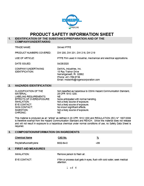
PRODUCT SAFETY INFORMATION SHEET1. IDENTIFICATION OF THE SUBSTANCE/PREPARATION AND OF THECOMPANY/UNDERTAKINGTRADENAME: SkivedPTFEPRODUCT NUMBERS COVERED: DW 200, DW 201, DW 218, DW 219USE OF ARTICLE: PTFE Film used in industrial, mechanical and electrical applications. DATEISSUED: 04/28/2020COMPANY/UNDERTAKING IDENTIFICATION: DeWAL Industries, Inc.15 Ray Trainor DriveNarrangansett, RI 02882Phone: 401-789-9736Email:******************************2. HAZARDS IDENTIFICATIONCLASSIFICATION OF THE MATERIAL: Not classified as hazardous to OSHA Hazard Communication Standard, 29 CFR 1910.1200.LABELINGREQUIREMENTS: NEEFFECTS OF OVEREXPOSURE: None anticipated with normal handling.INHALATION: Not a likely source of exposure.EYE CONTACT: Not a likely source of exposure.SKIN CONTACT: No known significant effects.INGESTION: Not a likely source of exposure.CHRONIC: NEThis material is produced as an “article” as defined in 20 CFR 1910.1200 and REGULATION (EC) N° 1907/2006 is therefore exempt from the Hazard Communication Standard and REACH. Since this material does not release and will not result in exposure to a hazardous chemical under normal conditions of use, no Safety Data Sheet is required.3. COMPOSITION/INFORMATION ON INGREDIENTSChemicalName CAS No. %Polytetrafluoroethylene 9002-84-0 >994. FIRST-AID MEASURESINHALATION: Remove person to fresh air.EYE CONTACT: If film or process dust gets in eyes, flush with cold water, seek medicalattention.1 of 6SKIN CONTACT: Not a likely medical issue, unless cut by the film, then treat as youwould a normal cut.INGESTION: Not a likely medical issue.5. FIRE-FIGHTING MEASURESFLASHPOINT: Noneo C (o F)FlammableLimits:LEL NA UEL NA AUTOIGNITIONTEMPERATURE: NEo C (o F)EXTINGUISHINGMEDIA: X WaterSprayX Foam X CO2X DryChemical X Other–SPECIAL FIRE FIGHTING PROCEDURES: When conditions are severe and thermal decomposition is possible, wear full protective clothing, including helmet, self-contained positive pressure breathing apparatus, bunker coat and pants, bands around arms and legs, full face mask and protective covering for any exposed areas of the head.UNUSUAL FIRE AND EXPLOSIONHAZARDS:Exposure to extreme heat may give rise to thermal decomposition.6. ACCIDENTAL RELEASE MEASURESPERSONALPRECAUTIONS: Observecautions from other sections of PSIS. Non-hazardous solid.ENVIRONMENTAL PRECAUTIONS: None known.CLEANING METHODS: Sweep or shovel into normal trash. Avoid creation of nuisance dust. 7. HANDLING AND STORAGEHANDLING: When working with this film, it is recommended that you wash yourhands thoroughly before smoking; dust created during processing canget into tobacco products and possibly lead to hazardousdecomposition products.STORAGE: Use normal storage procedures.8. EXPOSURE CONTROLS/PERSONAL PROTECTION8.1 Occupational Exposure Limits (OEL’s)Ingredient CAS # Agency Limit TypePolytetrafluoroethylene 9002-84-0 CMRG TWA(respirable dust): 5 mg/m3;2 of 6ACGIH : American Conference of Governmental Industrial HygienistsAIHA : American Industrial Hygiene AssociationCMRG : Chemical Manufacturer's Recommended GuidelinesOSHA : United States Department of Labor - Occupational Safety and Health AdministrationTWA: Time-Weighted-AverageSTEL: Short Term Exposure LimitCEIL: Ceiling8.2 Exposure ControlsFor any situation where the material might be exposed to extreme overheating, use appropriate local exhaust ventilation to reduce any possible thermal decomposition products. If local ventilation is not possible, userespiratory protection equipment.PROTECTION: None needed under normal conditions. If material is heated and odors RESPIRATORYare noticeable and/or irritating a respirator meeting NIOSHrequirements should be used. A qualified individual should evaluateeach situation.VENTILATIONLOCAL: Recommended for all industrial operations.GENERAL: Recommended for all industrial operations.PERSONALPROTECTIONHAND: Gloves would be recommended to help prevent abrasions and cutsfrom handling the film.EYE: Safety glasses with side-shields are recommended in all industrialoperations.SKIN: Gloves would be recommended to help prevent abrasions and cutsfrom handling the film.THERMAL HAZARDS Unlikely exposure.OTHER: Safety shower/eyewash in the area.9. PHYSICAL AND CHEMICAL PROPERTIESwhitefilmAPPEARANCE: SolidODOR: OdorlessSTATE: SolidPHYSICALo C (o F)BOILINGPOINT: NAMELTING POINT: 320 - 345˚Co C (o F)POINT: NAFREEZINGo C (o F)FLASHPOINT: NoneSOLUBILITY: In-SolubleWATERDENSITY: NAVAPORPRESSURE: NAVAPORSPECIFIC GRAVITY: 2.14 – 2.18 (Ref Std: Water = 1)COEFFICIENT: NAPARTITIONRATE: NAEVAPORATIONDENSITY: 2.14 – 2.18 g/cm3VISCOSITY: NAAUTO-IGNITION TEMPERATURE: No data available.ORGANIC COMPOUNDS: NAVOLATILEDECOMPOSITIONTEMPERATURE: No data available.VOLATILE: NAPERCENTH2O ELEMENT SOLVENT: NALESSVOCPH: NAFLAMMABILITY: NotClassified.3 of 610. STABILITY AND REACTIVITYSTABLEX UNSTABLECONDITIONS TO AVOID: Not determined.MATERIALS TO AVOID: Alkali and Alkaline earth metals.HAZARDOUSPOLYMERIZATION: May Occur X Does Not OccurHAZARDOUSDECOMPOSITIONPRODUCTS:Substance ConditionCarbonyl Fluoride At Elevated Temperatures – above 380˚CCarbon Monoxide At Elevated Temperatures – above 380˚CCarbon Dioxide At Elevated Temperatures – above 380˚CHydrogen Fluoride At Elevated Temperatures – above 380˚CPerfluoroisobutylene(PFIB) AtElevated Temperatures – above 380˚CToxic Vapor, Gas, Particulate At Elevated Temperatures – above 380˚CIf this product is exposed to extreme conditions of heat from misuse or equipment failure, toxic decomposition can occur.11. TOXICOLOGICAL INFORMATIONThis information may not be consistent with the material classification in Section 2 if specific ingredient classifications are mandated by a competent authority. In addition, toxicological data on ingredients may not be reflected in the material classification and / or the signs and symptoms of exposure, because an ingredient may be present below the threshold for labeling, an ingredient may not be available for exposure, or the data may not be relevant to the material as a whole.11.1 Information of Toxicological EffectsSIGNS AND SYMPTOMS OF OVEREXPOSURE: Based on information on the components, this material may produce the following health effects:Inhalation: Not a likely source of exposure.However, If overheated, Polymer Fume Fever could occur.Signs/Symptoms may include chest pain, shortness of breath, cough,malaise, muscle aches, increased heart rate, fever, chills, sweats,nausea and headache.Skin Contact: Mechanical Skin irritation: Abrasion or cuts from film handling.Eye Contact: Not a likely source of exposure.Ingestion: Not a likely source of exposure.TOXICOLOGICALDATA:Acute Toxicity Name Route ValueOverall Product Ingestion No Data Available.Polytetrafluoroethylene Dermal LD50 estimated to be >5000mg/ kgPolytetrafluoroethylene Ingestion LD50 estimated to be >5000mg/ kg4 of 6Skin IrritationPolytetrafluoroethylene No Significant Irritation.Serious Eye IrritationPolytetrafluoroethylene No Significant Irritation.Skin SensationSensitizing.Polytetrafluoroethylene NotRespiratory Sensationdata.Carcinogenicity Insufficientdata.Reproductive Toxicity Insufficientdata.Target Organs Insufficient 12. ECOLOGICAL INFORMATIONarechemically unreactive, non-toxic, non-water solubleproductsECOTOXICITY: Theseand non- biodegradable.13. DISPOSAL CONSIDERATIONNonePROPERTIESPHYSICAL/CHEMICALAFFECTING DISPOSAL:ENVIRONMENTAL TOXICITY DATA: NAWASTE DISPOSAL METHOD: Dispose of in accordance with applicable federal, state, provincial, andlocal laws and regulations.14. TRANSPORT INFORMATIONUN NUMBER: Not Regulated by DOT, IATA, IMDG, ARDUN PROPER SHIPPING NAME: Not Regulated by DOT, IATA, IMDG, ARDHAZARD CLASS (ES): Not Regulated by DOT, IATA, IMDG, ARDPACKING GROUP: Not Regulated by DOT, IATA, IMDG, ARDENVIRONMENTAL HAZARDS: Not Regulated by DOT, IATA, IMDG, ARD15. REGULATORY INFORMATION15.1 International Regulations: N/A15.2 U.S. Federal Regulations:This product is in compliance with the requirements of TSCA.TSCA(Toxic Substances Control Act):NACERCLA(Comprehensive EmergencyResponse, Compensation, and LiabilityAct):5 of 6SARA TITLE IIINA(Superfund Amendments andReauthorization Act):311/312 HAZARD CATEGORIES: Fire -No Pressure Hazard-No Reactivity-NoImmediate Hazard-No Delayed Hazard-NoINGREDIENTS: None.REPORTABLE31315.3 State Regulations: In compliance with State Regulations.16. OTHER INFORMATIONNA =Not Applicable FILE: 99472-DW 200, DW 201, 218, 219 PSIS-04282020NE = Not EstablishedNC = Not Classified PREPARED BY: Rogers Corporate EHSTHE INFORMATION CONTAINED HEREIN IS BASED ON DATA CONSIDERED ACCURATE. HOWEVER, NO WARRANTY IS EXPRESSED OR IMPLIED REGARDING THE ACCURACY OF THESE DATA OR THE RESULT TO BE OBTAINED FROM THE USE THEREOF. ROGERS CORPORATION ASSUMES NO RESPONSIBILITY FOR PERSONAL INJURY OR PROPERTY DAMAGE TO VENDEES, USERS OR THIRD PARTIES CAUSED BY THE MATERIAL. SUCH VENDEES OR USERS ASSUME ALL RISKS ASSOCIATED WITH THE USE OF THE MATERIAL.6 of 6。

一、概述TF系列通风柜是根据国家城乡建设环境保护部(85)城设字第124号档,编制的图集J930为主要内容,引用美国UL1805-93标准,最新编制QBMD.001-2004先进技术标准的基础上,结合我国实际积累多年经验研制而成的。
本TF系列通风柜具有结构合理、造型美观、操作方便、安全可靠、工作效率高、节能、补风、排风、性能优良,是国家监督检测、科研部门、大专院校及企事业单位理想的现代实验室装备。
二、通风柜型号定义2-1、型号命名:TF □□□—□分类(字母A、B、C)台面长度(数字12、15、18)空白:常风型、J:补风型 L:落地型通风柜2-2、分类A表示三面玻璃,全钢结构。
B表示单面玻璃,上箱体全钢,下箱体钢木结构。
C表示单面玻璃,全钢结构。
2-3、台面长度12表示1200mm×750mm×19mm15表示1500mm×750mm×19mm18表示1800mm×750mm×19mm台面标准宽度750mm(也可据用户要求宽度800mm、900mm),台面标准厚度由选择材质而定,详见通风柜标准明细表。
三、通风柜标准明细表参见通风柜标准明细表第6页四、通风柜安装方法4-1、按照指定位置摆正下箱体,调整4个地脚螺丝使箱体达到水平。
4-2、在下箱体的上面摆正台面,左右边沿达到一致,前后边沿以后部对齐为准,然后全面调整达到水平。
4-3、在台面上面,摆正上箱体,台面与上箱体和下箱体固定,并且用密封胶作好密封处理。
上好活动玻璃门、玻璃门配重,使玻璃门上下拉动自如。
4-4、接好上水、下水、电器电路。
4-5、配接好通风管路、风机,防雨罩、减振器。
4-6、实验室同时设有多台通风柜时,最好单独设计排风系统,可达到节能的目的。
如果采用集中排风时,应按照每台工作面风速参数的要求选择风机,如功率选择大于4KW以上应加装风机消音器,并按合理的型式进行布置。
4-7、排放有害气体时,需增加净化装置,对有害气体净化达到排放标准后方可排出。


SFH 221Silizium-Differential-Fotodiode Silicon Differential PhotodiodeLead (Pb) Free Product - RoHS Compliant2007-04-031Wesentliche Merkmale•Speziell geeignet für Anwendungen im Bereich von 400 nm bis 1100 nm •Hohe Fotoempfindlichkeit•Hermetisch dichte Metallbauform (ähnlich TO-5), geeignet bis 125 °C 1)•Doppeldiode von extrem hoher Gleichmäβigkeit Anwendungen •Nachlaufsteuerungen •Kantenführung •Industrieelektronik•…Messen/Steuern/Regeln“1)Eine Abstimmung der Einsatzbedingungen mit dem Hersteller wird empfohlen bei T A > 85 °C1)For operating conditions of T A > 85 °C please contact us.Typ Type Bestellnummer Ordering Code SFH 221Q62702P0270Features•Especially suitable for applications from 400 nm to 1100 nm •High photosensitivity•Hermetically sealed metal package (similar to TO-5), suitable up to 125 °C 1)•Double diode with extremely high homogeneousness Applications •Follow-up controls •Edge drives•Industrial electronics•For control and drive circuitsGrenzwerte Maximum RatingsBezeichnung Parameter SymbolSymbolWertValueEinheitUnitBetriebs- und Lagertemperatur Operating and storage temperature range Top; T stg– 40 … + 125°CSperrspannung Reverse voltage VR10VIsolationsspannung gegen Gehäuse Insulation voltage vs. package VIS100VVerlustleistung, T A = 25 °C Total power dissipation Ptot50mWKennwerte (T A = 25 °C, Normlicht A, T = 2856 K) für jede Einzeldiode Characteristics (T A = 25 °C, standard light A, T = 2856 K) per single diodeBezeichnung Parameter SymbolSymbolWertValueEinheitUnitFotoempfindlichkeit, V R = 5 VSpectral sensitivityS24 (≥ 15)nA/IxWellenlänge der max. FotoempfindlichkeitWavelength of max. sensitivityλS max900nmSpektraler Bereich der FotoempfindlichkeitS = 10% von SmaxSpectral range of sensitivityS = 10% of Smaxλ400 … 1100nmBestrahlungsempfindliche FlächeRadiant sensitive areaA 1.54mm2Abmessung der bestrahlungsempfindlichen Fläche Dimensions of radiant sensitive area L×BL×W0.7 × 2.2mm²Halbwinkel Half angle ϕ± 55Graddeg.Dunkelstrom, V R = 10 V Dark current IR10 (≤ 100)nASpektrale Fotoempfindlichkeit, λ = 850 nm Spectral sensitivity Sλ0.55A/W2007-04-0322007-04-033Maximale Abweichung der Fotoempfindlichkeit vom MittelwertMax. deviation of the system spectral sensitivity from the averageΔS± 5%Quantenausbeute, λ = 850 nm Quantum yieldη0.80Electrons Photon Leerlaufspannung, E v = 1000 Ix Open-circuit voltageV O 330 (≥ 280)mV Kurzschlu βstrom, E v = 1000 Ix Short-circuit current I SC 24μA Isolationsstrom, V IS = 100 V Insulation currentI IS 0.1 (≤ 1)nA Anstiegs- und Abfallzeit des Fotostromes Rise and fall time of the photocurrentR L = 1 k Ω; V R = 5 V; λ = 850 nm; I p = 25 μA t r , t f500nsDurchla βspannung, I F = 40 mA, E = 0 Forward voltageV F 1.0V Kapazität, V R = 0 V, f = 1 MHz, E = 0 CapacitanceC 025pF Temperaturkoeffizient für V O Temperature coefficient of V O TC V – 2.6mV/K Temperaturkoeffizient für I SC Temperature coefficient of I SCTC I 0.18%/K Rauschäquivalente Strahlungsleistung Noise equivalent power V R = 10 V, λ = 850 nmNEP1.0 × 10–13Nachweisgrenze, V R = 10 V, λ = 850 nm Detection limitD*1.2 × 10¹²Kennwerte (T A = 25 °C, Normlicht A, T = 2856 K) für jede EinzeldiodeCharacteristics (T A = 25 °C, standard light A, T = 2856 K) per single diode (cont’d)Bezeichnung ParameterSymbol Symbol Wert Value Einheit Unit W Hz -----------cm Hz ×W--------------------------2007-04-034OPTO SEMICONDUCTORSRelative Spectral SensitivityDark CurrentDirectional Characteristics S Photocurrent I P = f (Ev ), VR = 5 V CapacitanceTotal Power Dissipation Dark CurrentMaßzeichnungPackage OutlinesMaße in mm (inch) / Dimensions in mm (inch).2007-04-035LötbedingungenSoldering ConditionsWellenlöten (TTW)(nach CECC 00802)TTW Soldering(acc. to CECC 00802)OSRAM Opto Semiconductors GmbHWernerwerkstrasse 2, D-93049 Regensburg© All Rights Reserved.The information describes the type of component and shall not be considered as assured characteristics.Terms of delivery and rights to change design reserved. Due to technical requirements components may contain dangerous substances. For information on the types in question please contact our Sales Organization.PackingPlease use the recycling operators known to you. We can also help you – get in touch with your nearest sales office. By agreement we will take packing material back, if it is sorted. You must bear the costs of transport. For packing material that is returned to us unsorted or which we are not obliged to accept, we shall have to invoice you for any costs incurred.Components used in life-support devices or systems must be expressly authorized for such purpose! Critical components 1 , may only be used in life-support devices or systems 2 with the express written approval of OSRAM OS.1 A critical component is a component usedin a life-support device or system whose failure can reasonably be expected to cause the failure of that life-support device or system, or to affect its safety or effectiveness of that device or system.2 Life support devices or systems are intended (a) to be implanted in the human body, or (b) to support and/or maintain and sustain human life. If they fail, it is reasonable to assume that the health of the user may be endangered.2007-04-036分销商库存信息: OSRAMSFH 221。

Aluminum Electrolytic Capacitors CS SERIES1.ScopeThis sp ecification covers “CS Series” V-chip aluminum electrolytic capacitors.2.Reference StandardJapanese industrial Standard JIS C-5141 characteristics W and JIS C-5102 except as specified in this specification.3.Environmental Protection StandardComply with the EU directive 2002/95/EC.4.Operating Temperature Range-40︒C ~ +85︒C5.Voltage Range4 ~ 100V6.Capacitance Range0.1~ 1500μF7.Capacitance Tolerance±20% at 120Hz, 20︒C8.Leakage Current1 ≤ 0.01 CV or 3 (μA) whichever is greater (after2 minutes)9.Tan δMeasurement frequency: 120Hz, Temperature: 20︒C10.Stability at Low TemperatureMeasurement frequency: 120Hz11.Load Life12. Shelf LifeAfter leaving capacitors under no load at 85︒C for 1000 hours, they meet the specified value for load life characteristics listed above.13. Resistance to Soldering HeatAfter reflow soldering according to Reflow Soldering Condition (see page 5) and restored at room temperature, they meet the characteristics listed.14. MarkingCapacitors shall be legibly marked with the following: 1) M anufacture’s mark2) R ated voltage and nominal capacitance (6.3 voltage shall be marked with 6 voltage) 3) N egative polarity 4) M arking: Black15. Drawing (Unit: mm)(∅4~∅6.3)(∅8, ∅10) Aluminum Electrolytic Capacitors CS SERIESPlastic platformcsSeries Capacitance Rated V oltage16. Dimensions (Unit: mm)17. Taping SpecificationsApplicable standard JIS C0806(CS, CK, SC, CN, KP, LZ, KZ, FZ, EL, KL, KH, HU series) Carrier Tape17.1. Drawing 1 (for ∅4 ~ ∅10)Dimension17.2. Drawing 2 (for ∅12.5 ~ ∅16)Dimension (Unit: mm)17.3. Reel318. Lead-free Reflow Soldering ConditionA. Recommended Conditions for Reflow Soldering(1)A thermal condition system such as infrared radiation (IR) or hot blast should be adopted, and vapor heattransfer systems (VPS) are not recommended.(2)Reflow soldering should be performed one time. If the capacitor has to be reflowed twice, 30 minutesmust be layout between each time.(3)For lead-free type reflow soldering, please observe proper conditions below:a)The time of preheating from 150°C to 200°C shall be within maximum 180 seconds;b)The time of soldering temperature at 217°C measured on capacitors' top shall not exceed tL (second);c)The peak temperature on capacitors' top shall not exceed Tp(°C), and the time within 5°C of actualpeak temperature shall not exceed tp (second).B. Classification Reflow ProfilePackage quantityTp21720025Temperature温度(︒C)C. Allowable Range of Peak TemperatureD. Recommended Land Size (Unit: mm)19. The Raw Materials of Lead Wire20. Explanation of Part Number1 2 3 4 5 6 7 8 9 10 11 12 13 14 Example: CS 1C 221 M - C R E 77Length (7.7mm) Case Diameter (∅6.3mm) Lead Process (Taping & Reel) Type (Chip) DashCapacitance Tolerance (±20%) Capacitance (220μF) V oltage (16V)Series (CS)SeriesV oltage (WV) Capacitance (μF)Cap. Tol. (%)TypeLead ProcessDia. (∅)Length (mm)21. Construction22. Frequency Coefficient of Allowable Ripple Curren23 Dimensions & Maximum Permissible Ripple CurrentElectrolytic paper Base plateAluminum caseAluminum foil (Anode & cathode foil) Rubber sealLead wireAluminum Electrolytic Capacitors CS SERIESAluminum Electrolytic Capacitors CS SERIESAllowable ripple current (mA rms) at 85℃120Hz24. General Information for ApplicationThe following precautions must be observed when using electrolytic capacitors.A)Circuit Design1)Please make sure that the environmental and mounting conditions to which the capacitor to be exposedare within the conditions specified in this catalogue.2)Operating temperature and applied ripple must be within the specifications.3)Appropriate capacitors, which comply with the life requirement of the products, should be selected whendesigning the circuit.4)Aluminum electrolytic capacitors are polarized. Do not apply reserve voltage or AC voltage. Please usenon-polarized capacitors for a circuit that can possibly see reserved polarity.Note: Non-polarizes capacitors cannot be used for AC voltage application.5)Do not use aluminum electrolytic capacitors in a circuit that requires rapid and very frequent charge ordischarge. In this type of circuit, it is necessary to use special design capacitors with extended life characteristics.6)Do not apply excess voltage.Pleased pay attention so that the peak voltage, which is DC voltage overlapped by ripple current, should not exceed the rated voltage.In the case where more than two aluminum electrolytic capacitors are used in series, please make sure that applied voltage should be lower than rated voltage should be applied to each capacitorequally using a balancing resistor in parallel with the capacitor.7)Outer sleeved of the capacitor is not guarantee as an electrical insulator. Do not use standard sleeve on acapacitor in applications that require electrical insulation. When the application requires special insulation, please contact our sales office for details.8)Capacitors must not be used under following conditions:(a) Capacitors must not be exposed to water (including condensation), brine or oil.(b) Ambient conditions that include toxic gases such as hydrogen sulfide, sulfurous acid, nitrous acid,chlorine, ammonium, etc.(c) Ambient conditions that expose the capacitor to ozone, ultraviolet ray and radiation.Severe vibration and physical shock conditions that exceed our specification.Vibration test condition:Vibration frequency range: 10~55~10HzSweep rate : 10~55~10Hz per minuteSweep method : logarithmicAmplitude or acceleration: 1.5 (max. acceleration is 10G)Direction of vibration : X, Y, Z directionTesting time : 2 hours per each directionShock is not applicable normally.If a particular condition is required, please contact our sales office.9)When designing a circuit board, please pay attention to the following:Make the pad spacing on the PC board matching with the lead space of the capacitor.There should not be any circuit pattern or circuit wire above the capacitor safety vent.10)The main chemical solution of the electrolyte and the separator paper in the capacitor are combustible.The electrolyte is conductive. When it comes in contact with the PC board, there is a possibility of pattern or short circuit between the circuit pattern, which could result in smoking or fire. Do not locate any circuit pattern beneath the capacitor end seal.11)Do not design a circuit board so that heat generating components are placed near an aluminum electrolyticcapacitor or reserve side of PC board (under the capacitor).12)Please refer to the pad size layout recommendations in our catalogue when designing in surface mountcapacitors.13)Electrical characteristics may vary depending on changes in temperature and frequency. Please considerthe variation when you design circuits.14)When you install more than 2 capacitors in parallel, consider the balance of current following in to thecapacitor.B)Mounting1)Once a capacitor has been assembled in the set and power applied, do not attempt to re-use the capacitorin other circuits or application.2)Electric potential between positive and negative terminal may exist as a result of returned electromotiveforce, so please discharge the capacitor using 1KΩ resistor.3)Leakage current of the parts that have stored for long period may increase. When leakage current hasincreased, please perform a voltage treatment using a 1KΩ resistor.4)Please confirm rating and polarity before installing capacitor on the PC board.5)Be careful not to deform the capacitor during installation.6)Please confirm that the lead spacing of the capacitor matches the pad spacing of the PC board prior toinstallation.7)Please pay attention to the mechanical shock to the capacitor by suction nozzle of the automatic insertionmachine or automatic mounted, or by product checker, or by centering mechanism.8)Reflow soldering: please see “Lead –free Reflow Soldering Condition”.9)Do not tilt, lay down or twist the capacitor body after the capacitors are soldered to the PC board.10)Do not carry the PC board by grasping the soldered capacitor.11)Please do not allow anytime to touch the capacitor after soldering. If PC board are stored in stack, pleasemake sure PC board or the other components do not touch the capacitor. The capacitor shall not be effected by any radiated heat from the soldered PC board or other components after soldering.12)CleaningDo not clean capacitors with halogenated cleaning agent. However, if it is necessary to clean withhalogenated cleaning agent, please contact our sales office.Recommended cleaning method: Applicable : Any type, any ratingsCleaning agents : Pine Alpha ST-100S, cleaning through 750H/750L/710M, Sanelek B-12, AquaCleaner 210SEP, Techno Care FRW14~17, Isopropyl Alcohol.Cleaning condition: Total cleaning time shall be within 5 minutes by immersion, ultrasonic or othermethod. Temperature of the cleaning agent shall be 60︒C or lower. Aftercleaning, capacitors should be dried using hot air for minimum of 10 minutesalong with the PC board. Hot air temperature should be below the maximumoperating temperature of the capacitor. Insufficient dry after water rinse maycause appearance problems, sleeve shirk, bottom- plate bulge and such.③ Avoid using ozone destructive substance for cleaning agents to concern about global environment.④ Please consult us regarding other cleaning agents or cleaning methods.C)In The Equipment1) Do not directly touch terminal by hand.2) Do not short between terminal by conductor, nor spill conductible liquid such as alkaline or acidic solutionon or near the capacitor.3) Please make sure that the ambient conditions where the set is installed will be free from spilling water or oil,direct sunlight, ultraviolet rays, radiation, poisonous gases, vibration or mechanical shock.D)Maintenance and InspectionPlease periodically inspect the aluminum capacitors that are installed in industrial equipment. The following Items should be checked:Appearance: Remarkable abnormality such as vent operation, leaking electrolyte etc.Electrical characteristic: Capacitance, dielectric loss tangent, leakage current etc., which are specified in this catalogue.E)In an Emergency1) If you see smoke due to operation of safety vent, turn off the main switch or pull out the plug from theoutlet.2) Do not draw your face to the safety vent since gas over 100︒C will be emitted when the safety vent operates.If the gas has entered your eyes, please flush your eyes immediately in pure water. If you breathed the gas immediately wash out your mouth and throat with water. Do not ingest electrolyte. If your skin is exposed to electrolyte, please wash it away using soap and water.Aluminum Electrolytic CapacitorsF)Storage1)Do not keep capacitor in high temperature and high humidity.Storage conditions should be:Temperature : +5︒C ~ +35︒CHumidity : Lower than 75%Place : Indoor2) Avoid ambient conditions where capacitors can be covered with water, brine or oil.3) Avoid ambient conditions where capacitors are exposed to poisonous gases such as hydrogen sulfide,sulfurous acid, nitrous acid, chlorine, ammonium etc.4) Do not keep capacitor in conditions that expose the capacitor to ozone, ultraviolet ray or radiation.G)DisposalPlease dispose capacitors in either of the following ways:1)Incinerate capacitors after crushing parts or making a hole on the capacitor body.2)Bury capacitors in the ground. Please have a disposal specialist do it.25. NoteAll design and specifications are for reference only and is subject to change without prior notice. If any doubt about safety for your application, please contact us immediately for technical assistance before purchase.11。