THB6128-ETC (1)清晰版
- 格式:pdf
- 大小:425.19 KB
- 文档页数:17
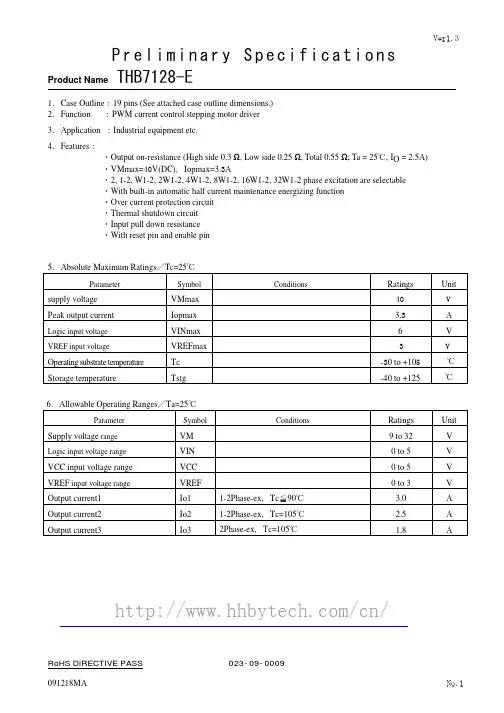
Ver1.3 P r e l i m i n a r y S p e c i f i c a t i o n s Product Name THB7128-E1.Case Outline:19 pins (See attached case outline dimensions.)2.Function :PWM current control stepping motor driver3.Application :Industrial equipment etc.4.Features:・Output on-resistance (High side 0.3 Ω, Low side 0.25 Ω, Total 0.55 Ω; Ta = 25℃, I O = 2.5A)・VMmax=40V(DC),Iopmax=3.3A・2, 1-2, W1-2, 2W1-2, 4W1-2, 8W1-2, 16W1-2, 32W1-2 phase excitation are selectable・With built-in automatic half current maintenance energizing function・Over current protection circuit・Thermal shutdown circuit・Input pull down resistance・With reset pin and enable pin5.Absolute Maximum Ratings/Tc=25℃Parameter Symbol Conditions Ratings Unit supply voltage VMmax 40 V Peak output current Iopmax 3.3 A Logic input voltage VINmax 6 V VREF input voltage VREFmax 3 V Operating substrate temperature Tc -30 to +105℃Storage temperature Tstg -40 to +125 ℃6.Allowable Operating Ranges/Ta=25℃Parameter Symbol Conditions Ratings Unit Supply voltage range VM 9 to 32 V Logic input voltage range VIN 0 to 5 V VCC input voltage range VCC 0 to 5 V VREF input voltage range VREF 0 to 3 V Output current1 Io1 1-2Phase-ex,Tc≦90℃ 3.0 A Output current2 Io2 1-2Phase-ex,Tc=105℃ 2.5 A Output current3 Io3 2Phase-ex,Tc=105℃ 1.8 A/cn/RoHS DIRECTIVE PASS023-09-00097.Electrical Characteristics/Tc=25℃, VM=24V, VREF=1.5VRatings Parameter Symbol Conditionsmin. typ. max.UnitStandby mode current drain IMstn VCC=”L”100µACurrent drain IM VCC=”H”,ENABLE="H"No Load 3.3 4.6mAThermal shutdown temperature TSDDesign guarantee 150 180 210 ℃Thermal hysteresis width∆TSDDesign guarantee 40 ℃IinL1 VIN=0.8V 3 8 15µALogic pin input currentIinH1 VIN=5V 30 50 70µALogic input high-level voltage Vinh 2.0 V Logic input low-level voltage Vinl 0.8 V Chopping frequency Fch C1=100pF 58 83 108 kHzChopping frequency Iosc1 10µAVtup1 1 V Chopping oscillator circuitthreshold voltage Vtdown1 0.5 V VREF pin input voltage Iref VREF=1.5V,CLK=10kHz -0.5 µADOWN output residual voltage V olDO Idown=1mA,CLK=Low 40mVHold current switching frequency Falert 1.6 Hz Blanking time Tb1 1 µs Output blockRonu I O=2.0A, high-side ON resistance 0.30 0.42 ΩOutput on-resistanceRond I O=2.0A, low-side ON resistance 0.25 0.35 ΩOutput leakage current Ioleak VM=36V 50 µA Diode forward voltage VD ID=-2.0A 1.1 1.4 V Current setting reference voltage VRF VREF=1.5V, Current ratio 100%300 mV Output short-circuit protection blockTimer latch time Tscp 256 µs/cn//cn/8. Block diagram9.Application Circuit Example2 315 516 18 17 19 84 61214791113M3 M2 M1 VCC CLK5VVREFOSC1 SGND NFB NFA VMOUT2BOUT1B OUT2AOUT1A C1RFBRFAR2R1C2C3THB7128-E1 GND10 PGNDM3 M1 VCCENABLE M2 19 17 15OSC14 CW/CCW 218 16CLK 3 G ND 1PGND 10VREG2OSC2 FDTOutput pre stageOutput pre stageRegulator 2Regulator 1Current selectcircuitOutput pre stageOutput pre stageOutput control logicCurrent selectcircuitDecay Mode setting circuitOscillator10.Pin FunctionsPin No. Pin symbol Pin Functions1 GND Circuit GND2 CW/CCW Forward / Reverse signal input3 CLK Clock pulse signal input4 OSC1 Chopping frequency setting capacitor connection5 VREF Constant-current control reference voltage input6 SGND Signal GND7 OUT2B B phase OUTB output8 NFB B phase current sense resistance connection9 OUT1B B phase OUTA output10 PGND Power GND11 OUT2A A phase OUTB output12 NFA A phase current sense resistance connection13 OUT1A A phase OUTA output14 VM Motor supply connection15 VCC Chip enable input16 M1Excitation-mode switching pin17 M218 M319 ENABLE Output enable signal input/cn//cn/11.Description of functions(1) Excitation setting methodSet the excitation setting as shown in the following table by setting M1 pin, M2 pin and M3 pinInput signal Initial positionM3 M2 M1 MODE (Excitation )A phase currentB phase current L L L 2 Phase 100% -100% L L H 1-2 Phase 100% 0% L H L W1-2 Phase 100% 0% L H H 2W1-2 Phase 100% 0% H L L 4W1-2 Phase 100% 0%H L H 8W1-2 Phase 100% 0% H H L 16W1-2 Phase 100% 0% H H H 32W1-2 Phase 100% 0%The initial position is also the default state at start-up and excitation position at counter-reset in each excitation mode(2)Output current settingOutput current is set as shown below by the VREF pin (applied voltage) and a resistance value between NFA (B) pin and GND.I OUT = (VREF / 5) / NFA (B) resistance* The setting value above is a 100% output current in each excitation mode.(Example) When VREF=1.5V and NFA (B) resistance is 0.3 Ω, the setting current is shown below. I OUT = (1.5 V / 5) / 0.3 Ω = 1.0 A(3) Chip enable terminal/ VCC functionWhen Chip enable terminal/ V CC pin is at low levels, the IC enters stand-by mode, all logic is reset and outputis turned OFF.When Chip enable terminal/ V CC pin is at high levels, the stand-by mode is released(4) Step pin function(5) Forward / reverse switching functionCW/CCW OperationL CW H CCW(6) Output enable functionWhen the ENABLE pin is set Low, the output is forced OFF and goes to high impedance. However, the internallogic circuits are operating, so the excitation position proceeds when the CLK is input. Therefore, when ENABLE pin is returned to High, the output level conforms to the excitation position proceeded by the CLK input.(7) DECAY modeThe DECAY mode of the output current becomes only MIXED DECAY.(8) Chopping frequency setting functionChopping frequency is set as shown below by a capacitor between OSC1 pin and GND.Fch = 1 /(C1+20pF/10×10-6) (Hz)(Example) When Cosc1=100pF, the chopping frequency is shown below.Fch = 1 /((20+ 100)×10-12/10×10-6) (Hz)=83.3(kHz)Note・The 20pF is a stray capacitance which is involved by the package of THB7128-E.(9) Output short-circuit protection circuitBuild-in output short-circuit protection circuit makes output to enter in stand-by mode. This function prevents the IC from damaging when the output shorts circuit by a voltage short or a ground short, etc. When output short state is detected, short-circuit detection circuit starts the operating and output is once turned OFF. After the timer latch time (typ: 256µs), output is turned ON again. Still the output is at short state, the output is turned OFF and fixed instand-by mode.When output is fixed in stand-by mode by output short protection circuit, output is released the latch by setting Chip enable terminal/ V CC="L"(10) Output current tolerance/cn/(11) When mounting multiple drivers on a single PC boardWhen mounting multiple drivers on a single PC board, the GND design should mount a VCC decoupling capacitor, C2 and C3, for each driver to stabilize the GND potential of the other drivers. The key wiring points are as follows./cn//cn/Package Outline DiagramProduct NameTHB7128-ENo.Part Name Material TreatmentUnit mm ① Case EPOXY Tolerance ±0.4② SubstrateIMST SubstrateDon’t scale this drawing. ③ Lead Frame CuSn Control No. 016-09-0083Oct.21.2009 Newly preparedMachidaSakainote1:Mark for No.1 pin identification.note2:The form of a character in this drawing differs from that of HIC.note3:This indicates the date code. The form of a character in this drawing differs from that of HIC./cn/。
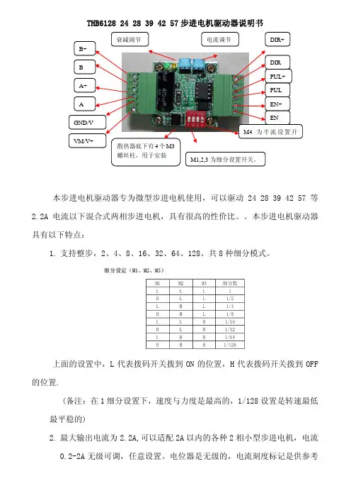
THB6128 24 28 39 42 57步进电机驱动器说明书本步进电机驱动器专为微型步进电机使用,可以驱动24 28 39 42 57等2.2A 电流以下混合式两相步进电机,具有很高的性价比。
本步进电机驱动器具有以下特点:1. 支持整步,2、4、8、16、32、64、128、共8种细分模式。
上面的设置中,L 代表拨码开关拨到ON 的位置,H 代表拨码开关拨到OFF 的位置.(备注:在1细分设置下,速度与力度是最高的,1/128设置是转速最低最平稳的)2. 最大输出电流为2.2A,可以适配2A 以内的各种2相小型步进电机,电流0.2-2A 无级可调,任意设置。
电位器是无级的,电流刻度标记是供参考用的。
如果你的电机是0.5A的调到0.4A与0.6A刻度的中间即可。
3.输入工作电压为DC9-32V.配有电源指示灯。
4.输入电路有防电源接反设计,更安全。
5.有自动半流开/关功能,工作方式更多样。
为开关M4设置。
6.有衰减模式控制功能。
在匹配不同型号的步进电机时,可以控制在不同的工作方式,使电机工作的更稳定,噪声,震动控制到最小。
为靠近LED 指示灯位置的电位器设置。
匹配电机时,调该电位器,使电机的震动与噪声最小即可。
7.行业标准的输入输出接口,兼容性强,可以支持共阴或共阳接法。
8.配有大型散热器,与安装固定柱,螺丝,使用更方便。
注意事项:1.驱动器匹配的电源容量最少都要有2A以上。
否则工作不稳定。
2.电机线不得AB相线交叉接,否则烧驱动器。
3.配PLC使用时,要加串2K左右限流电阻,否则烧驱动器。
附录:步进电机驱动使用注意事项1.关于电机驱动器电源的选用:每个驱动器的工作电源必须大于驱动器的最大驱动电流安数以上的容量。
平时工作作电流一般不是很大。
但电机在换向与启动时,一般电流会提升3-4倍左右或以上,视电机负载而定。
在选用电源时,要选用大容量的,浪涌冲击能力好的电源。
尽量选用开关电源供电。
在要求稳定性高的场合,不建议使用没有稳压功能的工频变压器整流滤波后的电源供电,因为这样会给步进电机的正常工作带来很多不稳定因素。

V1.1目录第1章概述 ............................................................................... 1-11.1引言1-11.2使用条件...................................................................................................................1-31.2.1电源.......................................................................................................................1-31.2.2环境温度与湿度 ....................................................................................................1-31.2.3预热.......................................................................................................................1-31.3体积与重量...............................................................................................................1-3第2章基本技术指标 ................................................................. 2-12.1技术指标...................................................................................................................2-12.2比较方法说明 ...........................................................................................................2-22.2.1面积比较 ...............................................................................................................2-22.2.2面积差比较............................................................................................................2-22.2.3电晕放电比较........................................................................................................2-32.2.4相位差比较............................................................................................................2-3第3章面板说明及显示说明....................................................... 3-13.1前面板说明...............................................................................................................3-13.2后面板说明...............................................................................................................3-23.3基本显示区域说明....................................................................................................3-3第4章测量显示键[DISP]说明.................................................... 4-14.1测量显示界面 ...........................................................................................................4-14.2测量显示界面的符号约定 ........................................................................................4-14.3测量显示界面主菜单下软键说明 .............................................................................4-14.3.1显示设置 ...............................................................................................................4-24.3.2比较设置 ...............................................................................................................4-24.3.3测量功能 ...............................................................................................................4-34.3.4辅助功能 ...............................................................................................................4-34.3.5统计功能 ...............................................................................................................4-44.3.6修改.......................................................................................................................4-4第5章测量设置键[SETUP]说明................................................. 5-15.1测量设置界面符号约定 ............................................................................................5-15.2测量设置界面 ...........................................................................................................5-15.2.1步骤(Step).........................................................................................................5-25.2.2模式(Mode).......................................................................................................5-25.2.3 CH1-CH8(TH2883S8-5),CH1-CH4(TH2883S4-5)通道配置..................................5-35.2.4采样速率(Samp)-模式选择为普通模式时可设置 .............................................5-35.2.5测试脉冲(Test Imp)-模式选择为普通模式时可设置.........................................5-35.2.6消磁脉冲(Erase Imp)-模式选择为普通模式时可设置.......................................5-35.2.7电压调整(Volt ADJ)-模式选择为普通模式时可设置 ........................................5-35.2.8起始电压(Start Volt)-模式选择为破坏模式时可设置........................................5-45.2.9终止电压(End Volt)-模式选择为破坏模式时可设置.........................................5-45.2.10电压步进(Volt Step)-模式选择为破坏模式时可设置 ......................................5-45.2.11比较器(Comparator)........................................................................................5-45.2.12位置(Position)(面积,面积差,电晕)..........................................................5-55.2.13位置(Position)(相位差) ................................................................................5-55.2.14差值(Limit)(面积,面积差,相位差)..........................................................5-55.2.15差值(Limit)(电晕)........................................................................................5-55.3波形设置界面 ...........................................................................................................5-65.3.1步骤(Step).........................................................................................................5-65.3.2模式(Mode).......................................................................................................5-75.3.3标波名()-模式选择为标准采样时有效...............................................5-85.3.4步骤名(StepNO.)-模式选择为标波复制和对比测试时有效..............................5-85.4内部文件界面 ...........................................................................................................5-85.5外部文件界面 ......................................................................................................... 5-11第6章系统设置键[SYSTEM]说明.............................................. 6-16.1系统界面...................................................................................................................6-16.1.1显示屏亮度(Brightness) .........................................................................................6-26.1.2合格/不合格显示(Pass/Fail) ..............................................................................6-26.1.3合格报警(Pass Alarm).......................................................................................6-26.1.4不合格报警(Pass Alarm) ...................................................................................6-26.1.5按键声音(Key Sound) .......................................................................................6-26.1.6拷屏区域(Hard Copy) .......................................................................................6-26.1.7密码(Password) .................................................................................................6-36.1.8 Language .................................................................................................................6-36.1.9风格(Theme) ..........................................................................................................6-36.1.10日期(Date) ......................................................................................................6-36.1.11时间(Time)......................................................................................................6-46.2参数界面...................................................................................................................6-46.2.1波形显示(Wave Disp)........................................................................................6-46.2.2触发模式(Trig Mode)........................................................................................6-56.2.3延迟时间(Delay Time) ......................................................................................6-56.3接口界面...................................................................................................................6-56.3.1 I/O ..........................................................................................................................6-66.3.2 TH2883S RS232C接口...........................................................................................6-66.3.3 USB通讯接口 ........................................................................................................6-86.3.4 LAN通讯接口...................................................................................................... 6-116.4关于界面................................................................................................................. 6-13第7章使用指南 ........................................................................ 7-17.1按键使用...................................................................................................................7-17.1.1滚轮的使用............................................................................................................7-17.1.2显示页面切换........................................................................................................7-17.2基本测量...................................................................................................................7-17.2.1无标准测试............................................................................................................7-27.2.2标波采样测试........................................................................................................7-27.3破坏测试...................................................................................................................7-27.4技术应用...................................................................................................................7-27.4.1测试对象 ...............................................................................................................7-27.4.2判据的选择............................................................................................................7-37.4.3判据的设置............................................................................................................7-37.4.4标准的选取............................................................................................................7-47.4.5面积差图 ...............................................................................................................7-4第8章命令参考 ........................................................................ 8-18.1命令结构...................................................................................................................8-18.2符号约定与定义 .......................................................................................................8-28.3命令参考...................................................................................................................8-38.3.1 DISPlay子系统命令...............................................................................................8-38.3.2 IVOLTage子系统命令 ...........................................................................................8-68.3.3 SRATE子系统命令................................................................................................8-88.3.4 COMParator子系统命令 ........................................................................................8-88.3.5 TRIGger子系统命令 ............................................................................................ 8-148.3.6 STATistic子系统命令 .......................................................................................... 8-158.3.7 WADJust子系统命令........................................................................................... 8-158.3.8 SWAVE 子系统命令 ........................................................................................... 8-168.3.9 FETCh?子系统命令.............................................................................................. 8-178.3.10 MEASure 子系统命令........................................................................................ 8-208.3.11 ABORt 子系统命令 ........................................................................................... 8-218.3.12 MMEMory 子系统命令 ..................................................................................... 8-228.3.13 MeasSTEP 子系统命令...................................................................................... 8-238.3.14 WaveSTEP 子系统命令 ..................................................................................... 8-248.4出错信息................................................................................................................. 8-26第9章分选接口使用说明 .......................................................... 9-19.1基本信息...................................................................................................................9-19.2电气特征...................................................................................................................9-29.2.1直流隔离输出........................................................................................................9-29.2.2直流隔离输入........................................................................................................9-39.3 HNADLER接口板跳线设置 .....................................................................................9-4第10章成套与保修 ................................................................. 10-110.1成套...................................................................................................................... 10-110.2保修...................................................................................................................... 10-1第1章概述感谢您购买和使用我公司产品,在您使用本仪器前请根据说明书最后一章“成套和保修”的事项进行确认,若有不符请尽快与我公司联系,以维护您的权益。
使用说明书OPERATION MANUALTH2816B Universal LCR MeterT o n g h u i E l e c t r o n i c s C o.,L t d.地址:常州市新北区天山路3号T E L:(0519)5132222,5113342F A X:(0519)5109972E M A I L:t o n g h u i@p u b.c z.j s i n f o.n e tH t t p://w w w.t o n g h u i.c o m.c n目 录1概 述....................................................................................................................................1-11.1引言............................................................................................................................1-11.2使用条件....................................................................................................................1-21.2.1电源 a.........................................................................................................1-21.2.2环境温度与湿度.............................................................................................1-21.2.3预热................................................................................................................1-21.2.4几点注意问题 !..........................................................................................1-21.3体积与重量................................................................................................................1-31.4安全要求....................................................................................................................1-31.4.1绝缘电阻........................................................................................................1-31.4.2绝缘强度........................................................................................................1-31.4.3泄漏电流........................................................................................................1-31.5电磁兼容性................................................................................................................1-3 2基本技术指标........................................................................................................................2-12.1测量功能....................................................................................................................2-12.1.1测量参数........................................................................................................2-12.1.2等效方式........................................................................................................2-12.1.3量程................................................................................................................2-22.1.4触发方式........................................................................................................2-22.1.5延时................................................................................................................2-22.1.6测试端方式....................................................................................................2-22.1.7测量速度........................................................................................................2-22.1.8基本精度........................................................................................................2-22.2测试信号....................................................................................................................2-32.2.1测试信号频率................................................................................................2-32.2.2测试信号电平................................................................................................2-32.2.3输出阻抗........................................................................................................2-32.2.4测量显示范围................................................................................................2-32.2.5测试信号电平监视.........................................................................................2-42.3功能............................................................................................................................2-42.3.1校正功能........................................................................................................2-42.3.2比较器功能....................................................................................................2-42.3.3参数显示........................................................................................................2-52.3.4文件功能........................................................................................................2-52.3.5其他功能........................................................................................................2-52.3.6接口功能........................................................................................................2-6 3面板及显示说明....................................................................................................................3-13.1前面板说明................................................................................................................3-13.3基本显示区域说明....................................................................................................3-33.4页面按键....................................................................................................................3-43.5各页面概略................................................................................................................3-43.5.1元件测量显示页面(Meas Display).........................................................3-43.5.2档号显示页面(BinNo. Disp)...................................................................3-53.5.3测量设置页面(Meas Setup).....................................................................3-53.5.4极限表设置页面(Limit Setup)...............................................................3-63.5.5系统配置页面(System Config)...............................................................3-6 4使用说明................................................................................................................................4-14.1基本操作....................................................................................................................4-14.2显示画面说明............................................................................................................4-24.2.1开机画面........................................................................................................4-24.2.2元件测量显示页面.........................................................................................4-34.2.3档号显示页面..............................................................................................4-104.2.4测量设置页面..............................................................................................4-124.2.5极限列表设置页面.......................................................................................4-174.2.6系统配置页面..............................................................................................4-21 5元件的正确测量....................................................................................................................5-15.1常用元件测量............................................................................................................5-15.2被测件的正确连接....................................................................................................5-15.2.1被测件连接....................................................................................................5-15.2.2消除杂散阻抗的影响.....................................................................................5-25.3电感器和变压器的测量.............................................................................................5-35.3.1电感器的正确测量.........................................................................................5-35.3.2变压器的正确测量.........................................................................................5-65.4电容器的正确测量....................................................................................................5-95.4.1电容器的频率依赖性.....................................................................................5-95.4.2关于小损耗(如云母电容器)的精确测量...............................................5-105.4.3电容器的电平依赖性...................................................................................5-115.4.4SMD电容器的测量........................................................................................5-11 6性能测试................................................................................................................................6-16.1测量准确度................................................................................................................6-16.1.1│Z│,L,C,R,X的准确度......................................................................6-16.1.2 D 准确度........................................................................................................6-16.1.3Q 准确度........................................................................................................6-26.1.4θ准确度........................................................................................................6-26.1.5Rp 准确度......................................................................................................6-26.1.6Rs 准确度......................................................................................................6-26.1.7准确度因子....................................................................................................6-36.2.1性能测试所用器件及设备.............................................................................6-66.2.2功能检查........................................................................................................6-66.2.3测试信号电平精度测试.................................................................................6-66.2.4频率精度测试................................................................................................6-76.2.5电容量C、损耗D精度测试..........................................................................6-76.2.6电感量L精度测试.........................................................................................6-76.2.7阻抗Z精度测试.............................................................................................6-7 7远程控制................................................................................................................................7-17.1RS232C接口说明.......................................................................................................7-17.1.1RS232C接口简介............................................................................................7-17.1.2与计算机通讯................................................................................................7-27.2GPIB 接口说明..........................................................................................................7-87.2.1GPIB总线.......................................................................................................7-87.2.2GPIB接口功能.............................................................................................7-107.2.3GPIB地址.....................................................................................................7-107.2.4GPIB总线功能.............................................................................................7-107.3数据格式..................................................................................................................7-11 8命令参考................................................................................................................................8-18.1命令结构....................................................................................................................8-18.1.1命令结构基本规则.........................................................................................8-18.1.2多重命令........................................................................................................8-28.1.3命令及参数的缩写规则.................................................................................8-28.1.4数值的单位及倍率.........................................................................................8-28.2符号约定与定义........................................................................................................8-48.3命令参考....................................................................................................................8-58.3.1DISPlay子系统命令......................................................................................8-58.3.2FREQuency子系统命令..................................................................................8-68.3.3VOLTage子系统命令......................................................................................8-78.3.4FUNCtion子系统命令....................................................................................8-88.3.5APERture子系统命令..................................................................................8-118.3.6TRIGger子系统命令....................................................................................8-128.3.7FETCh?子系统命令.......................................................................................8-148.3.8ABORt子系统命令........................................................................................8-148.3.9CORRection子系统命令..............................................................................8-158.3.10COMParator子系统命令..............................................................................8-178.3.11Mass MEMory子系统命令............................................................................8-208.3.12公用命令.....................................................................................................8-218.4出错信息..................................................................................................................8-22 9分选接口使用说明................................................................................................................9-19.2信号线定义................................................................................................................9-29.3电气特征....................................................................................................................9-69.3.1直流隔离输出................................................................................................9-69.3.2直流隔离输入................................................................................................9-89.4HANDLER接口板跳线设置..........................................................................................9-99.5HANDLER口操作.......................................................................................................9-10 10成套与保修 (I)10.1成套 (I)10.2保修 (I)1概 述感谢您购买和使用我公司产品,在您使用本仪器前首先请根据说明书最后一章“成套和保修”的事项进行确认,若有不符请尽快与我公司联系,以维护您的权益。
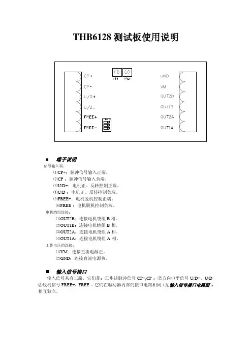
THB6128测试板使用说明
-
⏹端子说明
信号输入端:
⑴CP+:脉冲信号输入正端。
⑵CP-:脉冲信号输入负端。
⑶U/D+:电机正、反转控制正端。
⑷U/D-:电机正、反转控制负端。
⑸FREE+:电机脱机控制正端。
⑹FREE-:电机脱机控制负端。
电机绕组连接:
⑴OUT2B:连接电机绕组B相。
⑵OUT1B:连接电机绕组B-相。
⑶OUT2A:连接电机绕组A相。
⑷OUT1A:连接电机绕组A-相。
工作电压的连接:
⑴VM:连接直流电源正。
⑵GND:连接直流电源负。
⏹输入信号接口
输入信号共有三路,它们是:①步进脉冲信号CP+,CP-;②方向电平信号U/D+,U/D-③脱机信号FREE+,FREE-。
它们在驱动器内部的接口电路相同(见输入信号接口电路图),相互独立。

关于THB6128芯片应用注意事项
在使用THB6128过程中,有以下几点需要注意
1、芯片击穿的电压为36V(空载状态下),电机在运行时会产生的感应电动势,
电感越大、速度越快产生的电动势越大。
所以在选择电源时,需要把这考虑进去,推荐最高使用32V以下电源。
2、19脚OSC2外接的电容Cosc2和17脚DOWN的作用:
在Cosc2=1500PF时即当0.6S内没有脉冲输入(即CLK低于1.5Hz),DOWN 输出低电平,通过相连的电阻将VREF的电压拉低,进而减小芯片输出电流。
可通过减小这个电阻阻值而将锁定电流更进一步的降低。
3、20脚OSC1外接电容Cosc1和18脚FDT衰减模式控制端的作用
Cosc1的大小决定了衰减时间的长短,FDT有三种模式,Vfdt<0.8V时为快衰减,1.1V<Vfdt<3.1V时为混合衰减,3.5V<Vfdt时为慢衰减。
快、慢衰减时电流的走向见下图。
具体调整方式:先选好OSC1电容(即先确定衰减时间),再调整FDT电压,由低向高调,以电机运行平稳,噪音低、震动小时为佳。
4、在四个电机输出端与地之间需接入电阻Rx,阻值视供电电压而定,VM/Rx在
5mA左右即可。
作用是减弱毛刺对芯片的损坏。
5、在画芯片管脚的地线时要尽可能的粗,检测电阻和芯片之间的连线要短、粗,
两者的地线端相连也要短粗。
6、在靠近29脚(VCC)、2、5、11脚(VM)管脚处各放置1个0.1uf的电容。
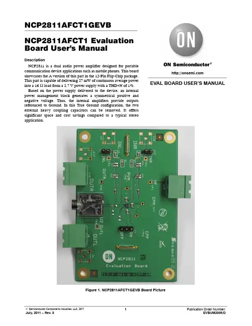
NCP2811AFCT1GEVB NCP2811AFCT1 Evaluation Board User's ManualDescriptionNCP2811 is a dual audio power amplifier designed for portable communication device applications such as mobile phones. This board showcases the A version of this part in the 12-Pin Flip-Chip package.This part is capable of delivering 27 mW of continuous average power into a 16 W load from a 2.7 V power supply with a THD+N of 1%.Based on the power supply delivered to the device, an internal power management block generates a symmetrical positive and negative voltage. Thus, the internal amplifiers provide outputs referenced to Ground. In this True Ground configuration, the two external heavy coupling capacitors can be removed. It offers significant space and cost savings compared to a typical stereo application.Figure 1. NCP2811AFCT1GEVB Board PictureEVAL BOARD USER’S MANUALFigure 2. NCP2811AFCT1GEVB Board SchematicFigure 3. NCP2811AFCT1GEVB Board Layout (Top View)Figure 4. NCP2811AFCT1GEVB Board Layout (Bottom View)Table 1. BILL OF MATERIALSManufacturer Manufacturer Reference Item Part Description Ref.PCBFootprintON Semiconductor NCP2811 1NCP2811 AudioAmplifier2SMD Resistor 10K W R1, R2, R3, R40603Panasonic ERJ−3GEY103VC1, C2, C3, C4, C50603Murata GRM185R60J105KA01 3Ceramic Capacitor1 m F 6.3 V X5R4Stereo Connector U2CUI Inc.SJ1−3515N5Jumper HeaderJ16100 mils Tyco Electronics / AMP5−826629−0 Vertical Mount, 2positions, 100mils6I/O Connector, 2J8, J19, J15200 mils Phoenix Contact1757242positions7Jumper Connector J18, J20400 mils Harwin D3082−B018Not Mounted R5, J9, J10, J6,J17,C6, C79Shorted R6, R70603NCP2811A OR NCP2811B CONFIGURATIONV.1NCP2811AConnect J11, J12. Put 10kohms on R1, R2, R3, R4. Disconnect J7, J14.V.1NCP2811BConnect J7, J14. Disconnect J11, J12, R1, R2, R3, R4.NCP2811 TEST PROCEDUREOutput Power:1.Set Vp = 3.6 V to power supply connector (J16).2.Set an 16 W load (resistance) on the output connectors (J8 and J17).3.With the function generator, set a single ended signal at 1 kHz and 0.5 Vrms input signal on the left and right inputs.Apply this signal J5 and J13 connectors.a.On the NCP2811A, as R1 = R2 = R3 = R4 = 10k, OUTL_C and OUTR_C will see 0.5 Vrms. Place anoscilloscope probe on each output. You should get 0.5 Vrms output signal with a “perfect sine wave”. That is to say no clipping at the minima and maxima of the sine wave.b.On the NCP2811B, the gain is internally set to -1.5 V/V, OUTL_C and OUTR_C will see 0.75Vrms. Place anoscilloscope probe on each output. You should get 0.75 Vrms output signal with a “perfect sine wave”. That isto say no clipping at the minima and maxima of the sine wave.Quiescent Current:Check the quiescent current. Place an 16 W load on each output (J8, J17); no input signal. Vp set to 3.6 V and J16 closed. You should measure around 6 mA.ADDITIONAL INFORMATIONTECHNICAL PUBLICATIONS :Technical Library: /design/resources/technical−documentation onsemi Website: ONLINE SUPPORT : /supportFor additional information, please contact your local Sales Representative at /support/sales。

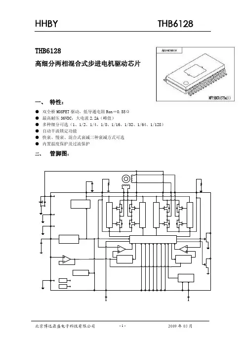
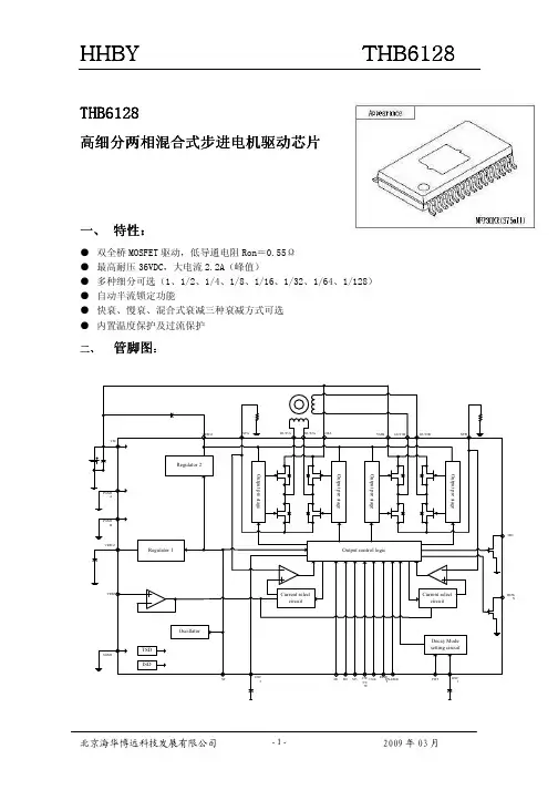
THB6128高细分两相混合式步进电机驱动芯片一、特性:●双全桥MOSFET 驱动,低导通电阻Ron=0.55Ω●最高耐压36VDC,大电流2.2A(峰值)●多种细分可选(1、1/2、1/4、1/8、1/16、1/32、1/64、1/128)●自动半流锁定功能●快衰、慢衰、混合式衰减三种衰减方式可选●内置温度保护及过流保护二、管脚说明:端子No 端子符号端子说明17 DOWN 通电锁定时输出端14/23 SGND 信号地20 OSC1 斩波频率设定电容连接端18 PFD 衰减模式选择电压输入端15 VREF 电流设定端11 VMB B 相电机电源连接端28 M1 细分设置端27 M2 细分设置端26 M3 细分设置端13 OUT2B B 相 OUTB 输出端10 NFB B 相电流检测电阻连接端9 OUT1B B 相 OUTB 输出端12 PGNDB B 相功率地7 OUT2A A 相 OUTA 输出端6 NFA A 相电流检测电阻连接端3 OUT1A A 相 OUTA 输出端4 PGNDA A 相功率地25 ENABLE 脱机信号控制端24 RESET 复位信号输入端5 VMA A 相电机电源连接端21 CLK 脉冲信号输入端22 CW/CCW 正/反转信号输入端19 OSC2 通电锁定检出时间设定电容连接端16 MO 位置检出Monitor 端30 VREG1 内部稳压器用电容连接端1 VREG2 内部稳压器用电容连接端2 VM 电机电源连接端29 ST/VCC 待机控制端三、电器参数1、电器特性Electrical Characteristics (Ta = 25°C, VREF =1.5 V, VM = 24 V)项目符号条件最小标准最大符号待机时消耗电流 IMstn ST=”L” 200 μA 消耗电流 IM ST=”H”、OE=”H”、无负载 4 mA TSD 温度 TSD 180 ℃Thermal Hysteresis 值ΔTSD 40 ℃逻辑端子输入电流 IinL1 VIN=0.8V 8 μAIinH1 VIN=5V 50 μA 逻辑输入“H”Level 电压 Vinh 2.0 V逻辑输入“L”Level 电压 Vinl 0.8 VFDT 端子“H”Level 电压 Vfdth 3.5 VFDT 端子“M”Level 电压 Vfdtm 1.1 3.1 VFDT 端子“L”Level 电压 Vfdtl 0.8 V斩波频率 Fch Cosc1=100pF 100 KHz OSC1 端子充放电电流 Iosc1 10 μA 斩波振荡电路 Vtup1 1 V电压阈值 Vtdown1 0.5 VVREF 端子输入电流 Iref VREF=1.5V -0.5 μA DOWN 输出残电压 VolDO Idown=1mA 400 mV MO 端子残电压 VolMO Imo=1mA 400 mV 通电锁定切换频率 Falert Cosc2=1500pF 1.6 Hz OSC2 端子充放电电流 Iosc2 TBD μA 通电锁定切换振荡电路 Vtup2 TBD V电压阈值 Vtdown2 TBD VREG1 输出电压 Vreg1 5 VREG2 输出电压 Vreg2 19 VBlanking 时间 Tbl 1 uS 输出输出ON 阻抗 Ronu Io=2.0A、上側ON 阻抗 0.3 Ω输出ON 阻抗 Rond Io=2.0A、下側ON 阻抗 0.25 Ω输出漏电流 Ioleak VM=36V 50 μA 二极管正向压降 VD ID=-2.0A 1 V电流设定基准电压 VRF VREF=1.5V、電流比100% 300 mV 输出短路保护Timer Latch 时间 Tscp 256 μs 2、最高额定值Absolute Maximum Ratings (Ta = 25°C)项目符号额定值符号最高耐压 VMmax 36 V最大输出电流 Iomax 2.2 A最高逻辑输入电压 VINmax 6 VVREF 最高输入电压 VREFmax 3 V工作环境温度 Topg -20~+85 ℃保存环境温度 Tstg -55~+150 ℃3、正常运行参数范围Operating Range (Ta = 30 to 85°C)参数符号最小典型. 最大单位逻辑输入电压 VIN 4.5 5.0 6 V电源电压 VM 9 − 36 V输出电流 Io − − 2 A电流设定端 VREF 0 − 3 V四、使用说明1、细分设定(M1、M2、M3)M1 M2 M3 细分数L L L 1H L L 1/2L H L 1/4H H L 1/8L L H 1/16H L H 1/32L H H 1/64H H H 1/1282、衰减模式设定PFD 为衰减方式控制端,调节此端电压可以选择不同的衰减方式,从而获得更好的驱动效果。
THB6128高细分两相混合式步进电机驱动芯片一、 特性:● 双全桥MOSFET驱动,低导通电阻Ron=0.55Ω● 最高耐压36VDC,大电流2.2A(峰值)● 多种细分可选(1、1/2、1/4、1/8、1/16、1/32、1/64、1/128) ● 自动半流锁定功能● 快衰、慢衰、混合式衰减三种衰减方式可选● 内置温度保护及过流保护二、 管脚图:三、 管脚说明:端子No 端子符号 端子说明17 DOWN 通电锁定时输出端14,23 SGND 信号地20 OSC1 斩波频率设定电容连接端18 FDT 衰减模式选择电压输入端15 VREF 电流设定端11 VMB B相 电机电源连接端28 M1 细分设置端27 M2 细分设置端26 M3 细分设置端13 OUT2B B相 OUTB输出端10 NFB B相 电流检测电阻连接端9 OUT1B B相 OUTB输出端12 PGNDB B相 功率地7 OUT2A A相 OUTA输出端6 NFA A相 电流检测电阻连接端3 OUT1A A相 OUTA输出端4 PGNDA A相 功率地25 ENABLE 脱机信号控制端24 RESET 复位信号输入端5 VMA A相 电机电源连接端21 CLK 脉冲信号输入端22 CW/CCW 正/反转信号输入端19 OSC2 通电锁定检出时间设定电容连接端16 MO 位置检出Monitor端30 VREG1 内部稳压器用电容连接端1 VREG2 内部稳压器用电容连接端2 VM 电机电源连接端29 ST/VCC 待机控制端四、 电器参数:1、最高额定值Absolute Maximum Ratings (Ta = 25°C)项目 符号 额定值 符号最高电源电压 VMmax 36V最大输出电流 Iomax 2.2A最高逻辑输入电压 VINmax 6VVREF最高输入电压 VREFmax 3V工作环境温度 Topg -20~+85℃保存环境温度 Tstg -55~+150℃2、正常运行参数范围Operating Range (Ta =30 to 85°C)参数 符号 最小 典型.最大 单位 逻辑输入电压 VIN 4.5 5.0 6 V电源电压 VM9 −36 V输出电流 Io−− 2 A电流设定端 VREF0 −3V3、电器特性Electrical Characteristics (Ta = 25°C, VREF =1.5 V, VM = 24 V)项目 符号 条件 最小 标准 最大 符号待机时消耗电流 IMstn ST=”L” 200 μA 消耗电流 IM ST=”H”、OE=”H”、无负载 4 mA TSD温度 TSD 180 ℃ Thermal Hysteresis值 ΔTSD 40 ℃ 逻辑端子输入电流IinL1 VIN=0.8V 8 μAIinH1 VIN=5V 50 μA 逻辑输入“H”Level电压 Vinh 2.0 V 逻辑输入“L”Level电压 Vinl 0.8 V FDT端子“H”Level电压 Vfdth 3.5 V FDT端子“M”Level电压 Vfdtm 1.1 3.1 V FDT端子“L”Level电压 Vfdtl 0.8 V 斩波频率 Fch Cosc1=100pF 100 KHz OSC1端子充放电电流 Iosc1 10 μA 斩波振荡电路Vtup1 1 V 电压阈值 Vtdown10.5 V VREF端子输入电流 Iref VREF=1.5V -0.5 μA DOWN输出残电压 VolDO Idown=1mA 400 mV MO端子残电压 VolMO Imo=1mA 400 mV 通电锁定切换频率 Falert Cosc2=1500pF 1.6 Hz OSC2端子充放电电流 Iosc2 TBD μA 通电锁定切换振荡电路Vtup2 TBD V 电压阈值 Vtdown2TBD V REG1输出电压 Vreg1 5 V REG2输出电压 Vreg2 19 V Blanking时间 Tbl 1 uS 输出Ronu Io=2.0A、上側ON阻抗 0.3 Ω 输出ON阻抗Rond Io=2.0A、下側ON阻抗 0.25 Ω 输出漏电流 Ioleak VM=36V 50 μA 二极管正向压降 VD ID=-2.0A 1 V 电流设定基准电压 VRF VREF=1.5V、電流比100% 300 mV 输出短路保护Timer Latch时间 Tscp 256 μs五、 使用说明1、细分设定(M1、M2、M3)M1 M2 M3 细分数L L L 1H L L 1/2L H L 1/4H H L 1/8L L H 1/16H L H 1/32L H H 1/64H H H 1/1282、衰减模式设定PDT为衰减方式控制端,调节此端电压可以选择不同的衰减方式,从而获得更好的驱动效果。
THB6128 Development Specification Proposal1. Application: PWM current control stepping motor driver2. Package: MFP30KR3. Features● 1 channel PWM current control stepping motor driver●BiCDMOS process IC●Output on-resistance( High side 0.3 Ω, Low side 0.25 Ω, Total 0.55 Ω; Ta = 25°C, Io = 2.0 A)●2, 1-2, W1-2, 2W1-2, 4W1-2, 8W1-2, 16W1-2, 32W1-2 phase excitation are selectable●Advance the excitation step with the only step signal input●Available forward reverse control●Iomax=2.2A●Over current protection circuit●Thermal shutdown circuit●Input pull down resistance●With reset pin and enable pin4. Absolute Maximum Ratings at Ta = 25°CUnit Parameter SymbolRatingsSupply voltage VMmax 40VOutput current Iomax 2.2 ALogic input voltage VINmax 6VVREF input voltage VREFmax 6VMO input voltage VMOmax 6VDOWN input voltage VDOmax 6VOperating temperature Topg -20 to +85°CStorage temperature Tstg -55 to +150°C5. Recommended Operating Range at Ta=25°CUnitRatingsParameter SymbolSupply voltage range VM 9 to 32VLogic input voltage range VIN 0 to 5VVREF input voltage range VREF 0 to 3V6. Electrical Characteristics at Ta =25°C, VM=24V, VREF=1.5VParameter Symbol Conditions mintypmaxUnit Standby mode current drain IMstn ST=”L” 70 μA current drain IM ST=”H”,OE=”H”, no load 4 mAThermal shutdown temperature TSD Designguarantee 180 °CThermal hysteresis width ΔTSD Designguarantee 40 °C IinL1 VIN=0.8V 8 μA Logic pin input currentIinH1 VIN=5V 50 μA Logic input high-levelvoltageVinh 2.0 VLogic input low-levelvoltageVinl 0.8V FDT pin high-level voltage Vfdth 3.5 V FDT pin middle-levelvoltageVfdtm 1.1 3.1V FDT pin low-level voltage Vfdtl 0.8V Chopping frequency Fch Cosc1=100pF 100 KHz OSC1 pin charge/dischargecurrentIosc1 10 μAVtup1 1 V Chopping oscillator circuitthreshold voltage Vtdown1 0.5 V VREF pin input voltage Iref VREF=1.5V -0.5 μA DOWN output residualvoltageV olDO Idown=1mA 400mV MO pin residual voltage V olMO Imo=1mA 400mVHold current switchingfrequency Falert Cosc2=1500pF 1.6 HzOSC2 pin charge/dischargecurrentIosc2 10 μAVtup2 1 V Hold current switchingfrequency threshold voltage Vtdown2 0.5 V REG1 output voltage Vreg1 5 V REG2 output voltage Vreg2 19 V Blanking time Tbl 1 uS Output blockRonu Io=2.0A, high-side ON resistance 0.3 ΩOutput on-resistanceRond Io=2.0A, low-side ON resistance 0.25 ΩOutput leakage current Ioleak VM=36V 50μA Diode forward voltage VD ID=-2.0A 1 VCurrent setting referencevoltage VRF VREF= 1.5V,Current ratio 100% 300 mVOutput short-circuit protection blockTimer latch time Tscp 256 μs7. PIN ARRANGEMENT (Proposal)8. Pin FunctionsPin No. Pin symbol Pin Functionscurrentoutput17 DOWN HoldingGND14,23SGND Signal20 OSC1 Chopping frequency setting capacitor connection18 FDT Decay mode select voltage input15 VREF Constant-current control reference voltage input11 VMB B phase motor supply connection28 M1 Excitation-mode switching pin27 M2 Excitation-mode switching pin26 M3 Excitation-mode switching pin13 OUT2B B phase OUTB output10 NFB B phase current sense resistance connection9 OUT1B B phase OUTA output12PGNDB B phase power GND7 OUT2A A phase OUTB output6 NFA A phase current sense resistance connection3 OUT1A A phase OUTA output4 PGNDA A phase power GND25 ENABLE Output enable signal input24 RESET RESET signal input5 VMA A phase motor supply connection21 CLK Clock pulse signal input22 CW/CCW Forward/Reverseinputsignal19 OSC2 Holding current detection time setting capacitor connectionmonitor16 MO Positiondetecting30 VREG1 Internal regulator capacitor connection1 VREG2 Internal regulator capacitor connectionconnectionpower2 VM Motorinput29 ST/VCC Chipenable9. Description of functions 9-1) Stand-by functionWhen ST/VCC pin is at low levels, the IC enters stand-by mode, all logic is reset and output is turned OFF. When ST/VCC pin is at high levels, the stand-by mode is released. 9-2) Step pin functionCLK pin step signal input allows advancing excitation step.9-3) Excitation setting methodSet the excitation setting as shown in the following table by setting M1 pin, M2 pin and M3 pin.Input Initial position M3 M2 M1 Mode(Excitation ) A phase current B phase current L L L 2 phase 100% -100% L L H 1-2 phase 100% 0% L H L W1-2 phase 100% 0% L H H 2W1-2 phase 100% 0% H L L 4W1-2 phase 100% 0% H L H 8W1-2 phase 100% 0% H H L 16W1-2 phase 100% 0% H H H 32W1-2 phase 100% 0%The initial position is also the default state at start-up and excitation position at counter-reset in each excitation mode.9-4) Output current settingOutput current is set as shown below by the VREF pin (applied voltage) and a resistance value between NFA (B) pin and GND. Iout = (VREF / 5)/ NFA (B) resistance* The setting value above is a 100% output current in each excitation mode.※(Example) When VREF=1.5V and NFA (B) resistance is 0.3 Ω, the setting current is shown below.Iout = (1.5 V / 5) / 0.3 Ω = 1.0 A9-5) Output enable functionWhen the ENABLE pin is set Low, the output is forced OFF and goes to high impedance. However, the internal logic circuits are operating, so the excitation position proceeds when the CLK is input. Therefore, when ENABLE pin is returned to High, the output level conforms to the excitation position proceeded by the CLK input.CLKB phMOHigh impeda nce outpu t9-6) Reset functionWhen the RESET pin is set Low, the output goes to initial mode and the excitation position is fixed in the initial position for CLK pin and CW/CCW pin input. MO pin outputs at low levels at the initial position. (Open drain connection)CLK RESET A phase out B phase ou MOInitial positionCW/CCW OperationL CWH CCWThe internal D/A converter proceeds by a bit on the rising edge of the step signal input to the CLK pin. In addition, CW and CCW mode are switched by CW and CCW pin setting.In CW mode, the B phase current is delayed by 90°relative to the A phase current. In CCW mode, the B phase current is advanced by 90°relative to the A phase current.9-8) DECAY mode settingCurrent DECAY method is selectable as shown below by applied voltage to the FDT pin.FDT voltage DECAY method3.5V to SLOW DECAY1.1V to 3.1Vor OPEN MIXED DECAYto 0.8V FAST DECAY9-9) DOWN, MO output pinOutput pin is an open drain connection. Each pin is turned ON at predetermined state and outputs at low levels.Pin state DOWN MOLowHoldingcurrent state Initial positionOFF Normalstate Non initial positionChopping frequency is set as shown below by a capacitor between OSC1 pin and GND.Fcp = 1 / (Cosc1 / 10×10-6) (Hz)(Example) When Cosc1=100pF, the chopping frequency is shown below.Fcp = 1 / (100×10-12 / 10×10-6) = 100 (kHz)9-11)Output current vector locus (1 step normalized 90°)Current setting ratio in each excitation mode9-12)Current wave example in each excitation mode (2 phase, 1-2 phase, W1-2 phase, 4W1-2 phase)2 phase excitation (CW mode)1-2 phase excitation (CW mode)CLKIA IB1000 -100 1000 -100 (%) (%)MOW1-2 phase excitation (CW mode) CLKIA IB1000 -1001000-100 (%) (%)MO4W1-2 phase excitation (CW mode)9-13) Output short-circuit protection circuitBuild-in output short-circuit protection circuit makes output to enter in stand-by mode. This function prevents the IC from damaging when the output shorts circuit by a voltage short or a ground short, etc. When output short state is detected, short-circuit detection circuit starts the operating and output is once turned OFF. After the timer latch time (typ: 256us), output is turned ON again. Still the output is at short state, the output is turned OFF and fixed in stand-by mode.When output is fixed in stand-by mode by output short protection circuit, output is released the latch by setting ST/VCC=”L”.9-14) Open-drain pin for switching holding currentThe output pin is an open drain connection.This pin is turned ON when no rising edge of CLK between the input signals while a period determined by a capacitor between OSC2 and GND, and outputs at low levels.The open-drain output in once turned ON, is turned OFF at the next rising edge of CLK.Holding current switching time (Tdown) is set as shown below by a capacitor between OSC2 pin and GND.Tdown = Cosc2 × 0.4×109 (s)(Example) When Cosc2=1500pF, the holding current switching time is shown below.Tdown = 1500 pF × 0.4×109 = 0.6 (s)10. Current control operation10-1) SLOW DECAY current control operationWhen FDT pin voltage is a voltage over 3.5 V , the constant-current control is operated in SLOW DECAY mode. (Sine-wave increasing direction)Coil cufch opC H AR G E CLKC u r r e n t m ode(Sine-wave decreasing direction)C oil c u rfch o pC L KS et t i n g C u r re n tEach of current modes operates with the follow sequence.● The IC enters CHARGE mode at a rising edge of the chopping oscillation.(A period of CHARGE mode (Blanking Time) is forcibly present in approximately 1 μs, regardless of the current value of the coil current(ICOIL)and set current (IREF)).● After the period of the blanking time, the IC operates in CHARGE mode until ICOIL ≥IREF. After that, the mode switchesto the SLOW DECAY mode and the coil current is attenuated until the end of a chopping period.At the constant-current control in SLOW DECAY mode, following to the setting current from the coil current may take time (or not follow) for the current delay attenuation.When FDT pin voltage is a voltage under 0.8V , the constant-current control is operated in FAST DECAY mode. (Sine-wave increasing direction)Coil cufch opCLKC ur r en t(Sine-wave decreasing direction)C oil c u rfch o pC L KS e t t i n g C u r r e n tEach of current modes operates with the follow sequence.● The IC enters CHARGE mode at a rising edge of the chopping oscillation.(A period of CHARGE mode (Blanking Time) is forcibly present in approximately 1 μs, regardless of the current value of the coil current (ICOIL) and set current (IREF)).● After the period of the blanking time, The IC operates in CHARGE mode until ICOIL ≥ IREF. After that, the modeswitches to the FAST DECAY mode and the coil current is attenuated until the end of a chopping period.At the constant-current control in FAST DECAY mode, following to the setting current from the coil current takes short-time for the current fast attenuation, but, the current ripple value may be higher.When FDT pin voltage is a voltage between 1.1 V to 3.1 V or OPEN, the constant-current control is operated in MIXED DECAY mode. (Sine-wave increasing direction)Coil cufch opC H AR G ES TPC u r r en t m ode(Sine-wave decreasing direction)C oi l c u rfc h opC L KS e t t i n g c C u r r e n t mEach of current modes operates with the follow sequence.●The IC enters CHARGE mode at a rising edge of the chopping oscillation.(A period of CHARGE mode (Blanking Time) is forcibly present in approximately 1 μs, regardless of the current value of the coil current (ICOIL) and set current (IREF)).●In a period of Blanking Time, the coil current (ICOIL) and the setting current (IREF) are compared.If an ICOIL < IREF state exists during the charge period:The IC operates in CHAGE mode until ICOIL ≥ IREF. After that, it switches to SLOW DECAY mode and then switches to FAST DECAY mode in the last approximately 1 μs of the period.If no ICOIL < IREF state exists during the charge period:The IC switches to FAST DECAY mode and the coil current is attenuated with the FAST DECAY operation until the end of a chopping period.The above operation is repeated.Normally, in the sine wave increasing direction the IC operates in SLOW (+FAST) DECAY mode, and in the sine wave decreasing direction the IC operates in FAST DECAY mode until the current is attenuated and reaches the set value and the IC operates in SLOW (+FAST) DECAY mode.11. Block diagram12. Wiring diagram13.Package Dimensions。