AP0809 V1.0
- 格式:pdf
- 大小:400.09 KB
- 文档页数:4

安裝說明Compact 5000 I/O 8 點安全灌入型數位輸入模組目錄編號 5069-IB8S 、5069-IB8SK5069-IB8S 和 5069-IB8SK 模組是 8 點安全灌入型輸入模組。
這些模組在符合 SIL CL3 和 PLe 、Cat. 4 在內等要求的安全控制網絡上提供安全I/O ,依照 IEC 61508、IEC 61511、IEC 62061 和 ISO 13849-1 中所規定。
您可以將 Compact 5000™ I/O 安全模組作為具有 CompactGuardLogix®5380 控制器的本地和遠端 I/O ,以及具有 GuardLogix 5580 控制器的遠端I/O 模組。
5069-IB8SK 模組的功能與 5069-IB8S 模組相同,但也具有保形塗層,可在惡劣環境中加以保護。
使用 Studio 5000 Logix Designer® 軟體設定模組。
Compact GuardLogix 5380 和 GuardLogix 5580 控制器必須使用韌體版本 32.011 或更新版本,才能使用Compact 5000 I/O 安全模組。
Compact 5000 I/O 安全模組使用生產者/消費者通訊模型。
生產者/消費者通訊模型是模組與其他系統裝置之間的一種智慧型資料交換,其中的每一個模組都不用先被輪詢即產生資料。
關於如何使用 Compact 5000 I/O 模組的詳細資訊,請參閱其他資源(第12頁)中所列的出版品。
變更摘要主題頁次關於模組5安裝系統5安裝拆卸式端子座7安裝模組8安裝端蓋9拆卸式端子座配線9從拆卸式端子座中斷電線9使用束線帶10開啟系統電源10移除模組10規格11其他資源12主題頁數移除配線圖有關如何為模組接上電線的資訊,請參閱其他資源(第12頁)中所列的出版物N/ACompact 5000 I/O 8 點安全灌入型數位輸入模組ATTENTION:Read this document and the documents listed in the Additional Resources section about installation, configuration and operation of this equipment before you install, configure, operate ormaintain this product. Users are required to familiarize themselves with installation and wiring instructions in addition to requirements of all applicable codes, laws, and standards.Activities including installation, adjustments, putting into service, use, assembly, disassembly, and maintenance are required to be carried out by suitably trained personnel in accordance with applicable code of practice.If this equipment is used in a manner not specified by the manufacturer, the protection provided by the equipment may be impaired.注意:在安装、配置、操作和维护本产品前,请阅读本文档以及“其他资源”部分列出的有关设备安装、配置和操作的相应文档。

ADC0809介绍1.主要特性1)8路8位A/D转换器,即分辨率8位。
2)具有转换起停控制端。
3)转换时间为100μs4)单个+5V电源供电5)模拟输入电压范围0~+5V,不需零点和满刻度校准。
6)工作温度范围为-40~+85摄氏度7)低功耗,约15mW。
2.内部结构ADC0809是CMOS单片型逐次逼近式A/D转换器,内部结构如图13.22所示,它由8路模拟开关、地址锁存与译码器、比较器、8位开关树型D/A转换器、逐次逼近3.外部特性(引脚功能)ADC0809芯片有28条引脚,采用双列直插式封装,如图13.23所示。
下面说明各引脚功能。
IN0~IN7:8路模拟量输入端。
2-1~2-8:8位数字量输出端。
ADDA、ADDB、ADDC:3位地址输入线,用于选通8路模拟输入中的一路ALE:地址锁存允许信号,输入,高电平有效。
START:A/D转换启动信号,输入,高电平有效。
EOC:A/D转换结束信号,输出,当A/D转换结束时,此端输出一个高电平(转换期间一直为低电平)。
OE:数据输出允许信号,输入,高电平有效。
当A/D转换结束时,此端输入一个高电平,才能打开输出三态门,输出数字量。
CLK:时钟脉冲输入端。
要求时钟频率不高于640KHZ。
REF(+)、REF(-):基准电压。
Vcc:电源,单一+5V。
GND:地。
ADC0809的工作过程是:首先输入3位地址,并使ALE=1,将地址存入地址锁存器中。
此地址经译码选通8路模拟输入之一到比较器。
START上升沿将逐次逼近寄存器复位。
下降沿启动A/D转换,之后EOC输出信号变低,指示转换正在进行。
直到A/D转换完成,EOC变为高电平,指示A/D转换结束,结果数据已存入锁存器,这个信号可用作中断申请。
当OE输入高电平时,输出三态门打开,转换结果的数字量输出到数据总线上。
DAC0832的中文资料手册典型D/A转换DAC0832芯片8位并行、中速(建立时间1us)、电流型、低廉(10~20元)①引脚和逻辑结构②DAC0832与微机系统的连接③应用举例。

(Chinese)DM-UL0001-04ULTEGRASW-R610SW-9071SW-R671ST-6870ST-6871FD-6870RD-6870SM-EW90-A SM-EW90-B EW-SD50EW-SD50-I SM-EWC2SM-JC40SM-JC41SM-BTR1SM-BTR2BT-DN110BT-DN110-A SM-BMR1SM-BMR2BM-DN100SM-BA01SM-BCR1SM-BCR2SM-BCC1经销商手册6870系列目录重要提示 (4)为了安全起见 (5)将使用到的工具列表 (15)安装 (17)电线接线图(总概念图) (17)电线接线图(连接器A侧) (19)安装双控手柄和刹车线 (23)前拨链器的安装 (26)安装后拨链器 (30)安装换档开关 (31)安装连接器A (39)安装连接器B (40)安装电池 (41)电线的连接 (47)连接器A的连接 (47)连接器B的连接 (49)通向双控手柄的连接 (55)在车架内为连接器B和电线布线 (57)中轴的安装 (58)卡箍的安装 (59)连接的确认 (60)电线的拆卸 (61)调整 (64)后拨链器的调整 (64)前拨链器的调整 (69)调整手柄行程 (74)给电池充电 (76)部件名称 (76)充电方法 (78)当无法充电时 (80)与个人电脑的连接和通信 (83)E-TUBE PROJECT中的可自定义设置 (83)保养 (85)更换支架外套 (85)铭牌的更换 (85)支架本体和手柄本体的拆卸 (86)安装按钮组件 (87)支架组件和手柄组件的组装 (89)导轮的更换 (90)安装B轴 (91)•经销商手册主要适合专业自行车技工使用。
对于未接受自行车安装专业培训的使用者,请勿试图利用经销商手册自行安装零部件。
如果您对手册信息的任意部分不太清楚,请勿进行安装。
请咨询购买地或当地自行车经销商地点寻求帮助。
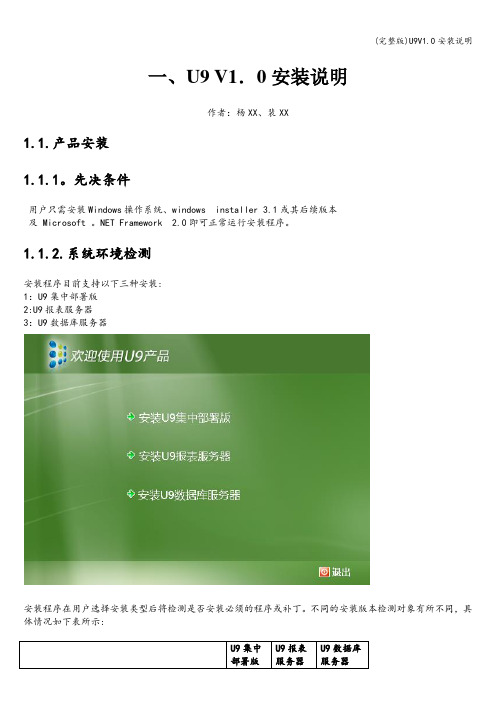
一、U9 V1.0安装说明作者:杨XX、裴XX1.1.产品安装1.1.1。
先决条件用户只需安装Windows操作系统、windows installer 3.1或其后续版本及 Microsoft 。
NET Framework 2.0即可正常运行安装程序。
1.1.2.系统环境检测安装程序目前支持以下三种安装:1:U9集中部署版2:U9报表服务器3:U9数据库服务器安装程序在用户选择安装类型后将检测是否安装必须的程序或补丁。
不同的安装版本检测对象有所不同,具体情况如下表所示:U9集中部署版U9报表服务器U9数据库服务器Windows 2003及其 Service Pack 2或更高版本是是是Internet Explorer 7。
0或更高版本是否否Microsoft SQL Server 2005及Service Pack 2否是是Microsoft Office 2007或更高版本是否否Microsoft 。
NET Framework 3。
0或更高版本是否否系统补丁NDP20—KB922770—X86是是否系统补丁NDP20—KB916002-x86是否否安装程序将在用户在用户选择安装类型后检测上述程序或补丁的安装情况:哪些已经安装,哪些没有安装。
只有当所有条件得到满足时安装程序才能继续运行。
1.1。
3.安装的实现安装过程如下所示(数据库服务器安装过程为例):1、带有U9 Logo的欢迎界面2、“最终用户许可协议”界面,用户只有在选择“接受《许可协议中的条款》”之后才可以继续运行安装程序。
3、自定义界面:告诉用户进行安装需要多少磁盘空间,帮助用户确认当前各个磁盘的总空间、可用空间、所需空间、差异空间等情况。
允许用户改变应用程序安装位置。
4、显示当前安装进程界面5、提示安装完成界面:用户可以在各个界面之间进行回退操作以改变选择。
1。
1。
4。
修复和卸载功能安装程序应具有修复功能,如果已安装的产品受到损坏(例如不小心删除了某些文件),可以通过重新运行安装程序进行自动检测缺少了哪些文件并进行修复。
UL Approvals Product Listing(For Use in Hazardous [Classified] Locations)for ASTRO® APX 8000XE Digital Portable RadiosDocument #: PMLN7375The APX 8000XE Land Mobile Radio Models for use in HAZ. LOC. are listed by UL to non-incendive standards:ISA 12.12.01-2015 and CAN/CSA C22.2 No. 213-15as safe for use in Class I, Division 2, Groups A,B,C,D;Class II, Division 2, Groups F,G;Class III, Division 2 Hazardous (Classified) Locations.Non-Incendive (Non Incendiaire)when used with Motorola Battery: PMNN4504A (Rated 7.4 V, 3400 mAh) or PMNN4505A (Rated 7.4 V,4850 mAh)MOTOROLA, MOTO, MOTOROLA SOLUTIONS and the Stylized M logo are trademarks or registered trademarks of Motorola Trademark Holdings, LLC and are used under license. All other trademarks are the property of their respective owners.© 2016 by Motorola Solutions, Inc. All Rights Reserved. 04/16*PMLN7375A*PMLN7375AMotorola Solutions, Inc.1303, E. Algonquin Rd., Schaumburg,IL 60196, U.S.A.Operational Cautions for Non-Incendive Equipment Radio unit must be ordered with the non-incendive option and shipped from the Motorola manufacturing facility with the hazardous location certification label. Radio will not be upgraded to this capability or labeled once it has been shipped.Operational CautionsOperational Warnings•DO NOT disassemble, heat above 100 °C ( 212 °F ), crush Array or incinerate Li-Ion Battery PMNN4504A and PMNN4505Ato avoid risk of fire, explosion and burns.•Failure to use a Motorola non-incendive battery oraccessory specifically certified for that radio unit willnegate the certification rating and could result in unsafecondition in hazardous areas.•DO NOT disassemble a non-incendive product in any way that exposes the internal circuits of the unit. This couldresult in unsafe condition in hazardous areas.•Unauthorized modification, or incorrect repair or service to the non-incendive product could adversely affect thecertification rating and result in unsafe condition inhazardous areas.•Use of non-Motorola parts or substitution of parts will voidthe non-incendive approval rating of the Motorola unit andcould result in unsafe condition in hazardous areas.The following Radio models, Batteries and Audio Accessories, can be used with the Radio model series.Note:Regional prefix: AA(NAG), AZ(Asia),LA(Latin America), or MD(Europe)APX 8000XEDescriptionModelALL BAND PORTABLE MODEL 1.5H91TGD9PW5AN ALL BAND PORTABLE MODEL 2.5H91TGD9PW6AN ALL BAND PORTABLE MODEL 3.5H91TGD9PW7ANAntennasDescriptionModelALL BAND (UHF, VHF, 700/800 MHz) GPS ANTENNA KT000026A011/4 WAVE (700/800 MHz) GPS STUBBY ANTENNA NAR6595A 700/800, UHF(380-520 MHz) GPS ANTENNAPMAS4001ABatteriesDescriptionModelBATT IMPRES 2 LIION UL2054 DIV2 R IP68 3400T PMNN4504A BATT IMPRES 2 LIION UL2054 DIV2 R IP68 4850TPMNN4505AAccessories for APX 8000XEDescriptionModelRemote Speaker Microphone with Jack HMN4101B Display Remote Speaker Microphone with JackHMN4103B Display Remote Speaker Microphone with Jack and Channel SelectorHMN4104B Secondary Audio Accessory for Display Remote Speaker MicrophoneRLN6424B XE RSM with High Temperature Cable NNTN8575A XE RSM Black with High Temparature CableNNTN8575ABLK IMPRES 2-Wire Surveillance Kit with translucent tube, programmable button, blackPMLN6129A Receive-Only Earpiece with Translucent Tube, 3.5 mm Jack, Short Coiled CableRLN4941ARemote Speaker Microphone, IMPRES Windporting IP55 3.5 mm jackPMMN4099A 1 Wire Receive-only Surveillance Kit with Translucent Tube, Black, Requires BDN6783RLN5313B Temple transducerRMN5116A Service Kit, 3pc Front Housing, Top Display , BlackKT000032A01Service Kit, 3pc Front Housing, Dual Display/Limited Keypad, BlackKT000032B01Service Kit, 3pc Front Housing, Dual Display/Full Keypad, Black KT000032C01Service Kit, 3pc Front Housing, Top Display , YellowKT000033A01Service Kit, 3pc Front Housing, Dual Display/Limited Keypad, YellowKT000033B01Service Kit, 3pc Front Housing, Dual Display/Full Keypad, Yellow KT000033C01Service Kit, 3pc Front Housing, Top Display , GreenKT000034A01Service Kit, 3pc Front Housing, Dual Display/Limited Keypad, GreenKT000034B01Service Kit, 3pc Front Housing, Dual Display/Full Keypad, Green KT000034C01Service Kit, 3pc Front Housing, Top Display , OrangeKT000035A01Service Kit, 3pc Front Housing, Dual Display/Limited Keypad, OrangeKT000035B01Service Kit, 3pc Front Housing, Dual Display/Full Keypad, Orange KT000035C01Service Kit, 3pc Front Housing, Top Display , RedKT000036A01Service Kit, 3pc Front Housing, Dual Display/Limited Keypad, RedKT000036B01Service Kit, 3pc Front Housing, Dual Display/Full Keypad, Red KT000036C01Service Kit, 3pc Front Housing, Top Display , BlueKT000037A01Service Kit, 3pc Front Housing, Dual Display/Limited Keypad, BlueKT000037B01Service Kit, 3pc Front Housing, Dual Display/Full Keypad, BlueKT000037C01Accessories for APX 8000XEDescriptionModel。

adc0809原理ADC0809是一款8位串行输入模数转换器(ADC),由National Semiconductor(现为德州仪器)开发和生产。
它的原理是将输入的模拟信号转换成对应的数字信号,用于数字系统的处理和分析。
ADC0809采用逐次逼近型模数转换技术,具有8个模拟输入通道,并且能完成8位精度的转换。
它的输入范围为0-5V,输入阻抗为100kΩ。
ADC0809包含一个8位逐次逼近型模数转换器、一个输入多路选择器、一个时钟驱动电路、一个控制逻辑和一个数据锁存器。
ADC0809的工作原理如下:首先,用户通过使用时钟信号来驱动转换器的工作。
时钟信号一般由控制器提供,控制器通过多个IO引脚向ADC0809发送指令信号。
时钟信号使得转换器按照指定的频率工作。
其次,输入模拟信号经过模拟开关输入,并通过输入多路选择器将选中的信号路径引入到采样保持电路中。
ADC0809的输入多路选择器可以选择8个不同的输入通道。
输入模拟信号经过采样保持电路后,被锁存并保持一段时间以进行后续处理。
然后,转换器根据锁存的模拟信号进行逐步逼近型模数转换。
逐序地,转换器首先将8位比较器的基准电压与DAC输出进行比较。
如果DAC输出高于基准电压,则比较器输出为高电平,否则为低电平。
比较器输出经过一个选择和存储逻辑单元(LCU),得到一个3位的二进制数,供数值控制逻辑(NCL)使用。
NCL 根据LCU的输出向DAC施加增量或减量,使得DAC输出逐渐逼近输入模拟量。
最后,转换器通过串行接口将转换后的数字结果通过数据锁存器传送到输出端,供控制器读取。
串行接口为8位的串行输出,由转换器的输出引脚提供。
转换后的数字结果可以进行进一步的数字处理和显示。
需要注意的是,ADC0809的转换精度和转换速率在一定程度上有一定的权衡。
为了提高转换精度,需要减小转换速率。
当转换速率较高时,转换精度可能会下降。
因此,在具体应用中需要根据需求选择合适的转换速率和精度。
们重在实际制做,太罗嗦的内容我就不说了,只讲些跟制做有关的最精炼的知识。
ADC0809是可以将我们要测量的模拟电压信号量转换为数字量从而可以进行存储或显示的一种转换IC。
下面是它的管脚图和逻辑图:管脚功能说明:IN0-IN7:模拟量输入通道。
就是说它可以分时地分别对八个模拟量进行测量转换。
ADDA-C:地址线。
也就是通过这三根地址线的不同编码来选择对哪个模拟量进行测量转换。
ALE:地址锁存允许信号。
在低电平时向ADDA-C写地址,当ALE跳至高电平后ADDA-C上的数据被锁存START:启动转换信号。
当它为上升沿后,将内部寄存器清0。
当它为下降沿后,开始A/D转换。
D0-D7:数据输出口。
转换后的数字数据量就是从这输出给S52的。
OE:输出允许信号,是对D0-D7的输出控制端,OE=0,输出端呈高阻态,OE=1,输出转换得到的数据。
CLOCK:时种信号。
ADC0809内部没有时钟电路,需由外部提供时钟脉冲信号。
一般为500KHzEOC:转换结束状态信号。
EOC=0,正在进行转换。
EOC=1,转换结束,可以进行下一步输出操作REF(+)、REF(-):参考电压。
参考电压用来与输入的模拟量进行比较,作为测量的基准。
一般REF(=)=5v REF(-)=0V。
下面我先给出ADC0809的时序图再说说它的工作过程:它的工作过程是这样的,①在IN0-IN7上可分别接上要测量转换的8路模拟量信号。
有人问了,可不可以只接一路?我就只想测一个模拟信号。
当然可了②将ADDA-ADDC端给上代表选择测量通道的代码。
如000(B)则代表通道0;001(B)代表通道1;111则代表通道7。
③将ALE由低电平置为高电平,从而将ADDA-ADDC送进的通道代码锁存,经译码后被选中的通道的模拟量送给内部转换单元。
④给START一个正脉冲。
当上升沿时,所有内部寄存器清零。
下降沿时,开始进行A/D转换;在转换期间,START保持低电平。
8V1090.00-21 General information•Modular mechanical design using plug-in modules•Integrated line filter•Integrated braking resistor•All connections are made using plug-in connectors•Integrated electronic restart inhibit2 Order dataTable 1: 8V1090.00-2 - Order dataTable 1: 8V1090.00-2 - Order data 3 Technical dataTable 2: 8V1090.00-2 - Technical data1)In the USA, TT and TN power mains are commonly referred to as "Delta/Wye with grounded Wye neutral".2)If the module is operated with a mains input voltage of 3x 230 VAC, then automatic nominal voltage detection doesn't work for the DC bus. The UDC_NOMINALparameter must be set to 325 [V] by the user in this case.3)Limit values from EN 61800-3 C3 (second environment).4)The permissible input voltage range is reduced when using motor holding brakes. The input voltage range should be selected so that the proper supplyvoltage for the motor holding brake can be maintained.5)The current consumption depends on the configuration of the ACOPOS servo drive.6)Valid in the following conditions: 400 VAC mains input voltage, nominal switching frequency, 40°C ambient temperature, installation elevation <500 m abovesea level.7)Value for the nominal switching frequency.8)If necessary, the stress of the motor isolation system can be reduced by an additional externally wired dv/dt choke. For example, the RWK 305 three-phasedv/dt choke from Schaffner () can be used. Important: Even when using a dv/dt choke, it is necessary to ensure that an EMC-compatible, low inductance shield connection is used!9)The module's electrical output frequency (SCTRL_SPEED_ACT * MOTOR_POLEPAIRS) is monitored to protect against dual use in accordance with ECregulation 428/2009 | 3A225. If the electrical output frequency of the module exceeds the limit value of 598 Hz uninterrupted for more than 0.5 s, then the current movement is aborted and error 6060 is output (Power element: Limit speed exceeded).10)OSSD (open signal switching device) signals are used to monitor signal lines for short circuits and cross faults.11)Continuous operation of ACOPOS servo drives at elevations ranging from 500 m to 2000 m above sea level is possible (taking the specified continuouscurrent reductions into consideration).12)Continuous operation of ACOPOS servo drives at ambient temperatures ranging from 40°C to max. 55°C is possible (taking the specified continuous currentreductions into consideration), but this will result in a shorter service life.4 Status indicatorsACOPOS servo drives are equipped with three LEDs for direct diagnostics:Figure 1: ACOPOS servo drives - Status indicatorsDescriptionGreen (lit)The module is operational andpresent and booted, no permanent or temporary errors).Green (blinking) 1)The module is not ready for operation.Examples:•No signal on one or both enable inputs•DC bus voltage outside the tolerance range•Overtemperature on the motor (temperature sensor)•Motor feedback not connected or defective•Motor temperature sensor not connected or defective•Overtemperature on the module (IGBT junction, heat sink, etc.)•Disturbance on networkOrange (lit)The module's power stage is enabled.Red (lit) 1)There is a permanent error on the module.Examples:•Permanent overcurrent•Invalid data in EPROMTable 3: LED status - ACOPOS servo drives1)Firmware V2.130 and higherIf no LEDs are lit, the ACOPOS servo drive is not being supplied with 24 VDC.Danger!After switching off the device, wait until the DC bus discharge time of at least five minutes has passed.The voltage currently on the DC bus must be measured with a suitable measuring device before be-ginning work. This voltage must be less than 42 VDC to rule out danger. An unlit Run LED does not indicate that voltage is not present on the device!4.1 LED statusThe following timing is used for the indication diagrams:Block size: 125 msRepeats after: 3000 msTable 4: Status changes when booting the operating system loaderTable 5: Error status with reference to the CAN plug-in module AC1101)Possible errors:- ACOPOS servo drive defect- Plug-in module defect- Plug-in module not inserted correctly in the slotTable 6: Error status with reference to the POWERLINK V2 plug-in module AC1141)Possible errors:- ACOPOS servo drive defect (plug-in module not recognized)- Plug-in module defect- Plug-in module not inserted correctly in the slot- Plug-in module functioning but not automatically recognized by the ACOPOS servo drive (old bootstrap loader)5 Dimension diagram and installation dimensionsHanging verticallyFigure 2: Dimension diagram and installation dimensions1)For proper air circulation, at least 80 mm clearance must be available above and below the ACOPOS servo drive.6 WiringFigure 3: ACOPOS 1022, 1045, 1090 - Pinout overview6.1 X1 - PinoutTable 7: X1 - Pinout1)The wiring is not permitted to exceed a total length of 30 m.6.2 X2 - PinoutTable 8: X2 - Pinout6.3 X3 - PinoutDanger!Servo drives are not permitted to be operated directly on IT and TN-S mains with a grounded phase conductor and protective ground conductor!Table 9: X3 - Pinout6.4 X4a, X4b - PinoutTable 10: X4a - Pinout1)If the holding brake is connected via an additional external relay contact (ground-in e.g. via the connections S1/S2) instead of via the internal transistor, thenthe internal quenching circuit has no effect! In this case, the customer must make sure that neither the relay contact nor the braking coil are damaged when switching off the brake. This can be done by interconnecting the coil or - better still - interconnecting the contact with a quenching circuit.Table 11: X4b - Pinout1)If the holding brake is connected via an additional external relay contact (ground-in e.g. via the connections S1/S2) instead of via the internal transistor, thenthe internal quenching circuit has no effect! In this case, the customer must make sure that neither the relay contact nor the braking coil are damaged when switching off the brake. This can be done by interconnecting the coil or - better still - interconnecting the contact with a quenching circuit.Danger!The connections for the motor temperature sensors and the motor holding brake are isolated circuits.Therefore, these connections are only allowed to be connected to devices or components with at least safe isolation in accordance with IEC 60364-4-41 or EN 61800-5-1.Caution!If B+ and B- are swapped when connecting the permanent magnet holding brakes, then the brakes cannot be opened! ACOPOS servo drives cannot determine if a holding brake is connected with reverse polarity!6.4.1 Wiring the connections for the motor holding brakeThe supply, activation and monitoring of the output for the motor holding brake can take place via the X4a connector in three different ways:Table 12: Activation for the external holding brake1)Both jumpers are already on the X4a connector delivered with the ACOPOS servo drives.2)External potential-free contacts can be connected between S1 and S2 as well as between S3 and S4. This makes it possible to activate the holding brakeusing an external safety circuit independent of the control integrated in the ACOPOS servo drive.3)The parameters are set using ParID 90 (1 ... internal monitoring active; 5 ... internal monitoring not active).4)Deactivation takes place using ParID 90 (5 ... internal monitoring not active).8V1090.00-2 6.5 X5 - PinoutTable 13: X5 - Pinout6.6 Additional protective ground connection (PE)The protective ground conductor is connected to the M5 threaded bolt provided using a cable lug.Terminal cross sectionsCable lug for M5 threaded boltTable 14: Protective ground conductor (PE) ACOPOS 1022, 1045, 1090Danger!Before turning on the servo drive, make sure that the housing is properly connected to ground (PE rail).The ground connection must be established even when testing the drive or operating it for a short time!8V1090.00-26.7 Input/Output circuit diagramFigure 4: TriggerFigure 5: LimitFigure 6: Enable8V1090.00-2Figure 7: ACOPOS 1022, 1045, 1090 - Input/Output circuit diagram。
任何6900都可以EVDO温馨提示:1:所谓的朗通数码官方版,只是用来更新prl和刷redio以及导入qpst文件的一个过渡,刷完之后同学们可以刷回自己喜欢的rom,只要带支持EVDO 的ROM就可以,比如Z大就有分RUIM和EVDO版本的rom下载。
2:以下教程是本人好几部手机遇到各类问题的总结,因为公司是电信卡,所以公司有不下15部6900手机。
有V版和T版,唉反正我感觉只是壳子不一样,不全是一家淘宝买的。
教程均为实际操作所得经验,仅供各位同学参考,如无法解决请跟帖说明,我会根据我的实际情况分析并及时更新。
3:如果遇到各类问题无法使用的,请刷回原来的redio并通过史上最强---改卡教程。
先用,并跟帖说明遇到的问题。
以便参考。
望能帮大家上EVDO(11月24日)更新,解决的问题:一: 00005导入时出现类似{"Tum on the LPM failed, Please restart your mobile phone click ok"}的错误。
或者导入无效的同学,请看 18二: esn为00000000导致prl好qpst问题,或刷机过程中出现问题,请看 19 (esn为00000000同时evdo成功的同学飘过)三: qpst中导入 36DC27C0_sp1 和 36DC27C0_sp.rl1 文件错误。
请看 20(11月17日)修改,可解决的问题:一:0005 无法通过的。
请看第10条。
已经重新说明0005无法通过的原因。
二:如果在仅EVDO模式无法通过的人,建议打电话到10000,让服务台帮忙把3G上网先关闭然后重新开通。
(我这有一张卡就是一直在仅ev下也过不了,换我自己的卡立刻可以,所以我打10000,让服务台重新开通。
如果以前从来就没有用过ev或者不知道自己是否已经开通evdo的同学,不妨打下10000 咨询.以免浪费时间)三:朗通数码官方版地址已更新四:没有小容量TF卡的同学,请把0005文件靠边到手机内存,经测试可行。
3-Pin Microprocessor Reset CircuitsDescriptionThe AP0809microprocessor supervisory circuit can be used to monitor the power supplies in microprocessor and digital systems.It provides a reset to the microprocessor during power-up,power-down,and brown-out conditions.The function of the AP0809is to monitor the V CC supply voltage,and assert a reset signal whenever this voltage declines below the factory-programmed reset threshold. The reset signal remains asserted for250ms after V CC rises above the threshold.The AP0809has an active-low RESET output.With a low supply current of only2μA(Typ.),the AP0809are ideal for use in portable equipment.The AP0809is available in the3-pin SOT23package. Applications●Microprocessor Systems●Computers●Controllers●Intelligent Instruments●Portable/Battery-Powered Equipment●Automotive Features●Precise monitoring of2.7V,3.0V,3.3V and5.0Vsupplies●140ms min.Power-On Reset pulse width,250mstypical,has an active-low RESET Output●Guaranteed RESET Output valid for V CC≥1.1V●Low Supply Current,2μA Typ.●Available in small SOT23package●No external components needed●Specified over full temperature range-40°Cto+105°CPackage Figure3Function DigramAbsolute Maximum RatingsV CC………………………………….…...–0.3V to6.0V RESET.………………………...–0.3V to(VCC+0.3V) Input Current at V CC………………..……………..20mA Output Current:RESET.………….……………...20mA Rate of Rise at V CC………………..…………...100V/µs Power Dissipation(T A=70°C)……….………..320mW (Derate4mW/°C above70°C)Operating Temperature Range………….–40°C to105°C Storage Temperature Range…………….–65°C to160°C Lead Temperature(soldering,10sec)…………...300°CThese are stress ratings only and functional operation is not implied.Exposure to absolute maximum ratings for prolonged time periods may affect device reliabilityElectrical CharacteristicsUnless otherwise noted V CC is over the full voltage range,T A=–40°C to105°C.Typical values at T A=25°C,V CC=5V for L/M/J devices,V CC=3.3V for T/S devices and V CC=3V for R devices.Parameter Symbol Conditions Min Typ Max UnitsInput V oltage (V CC)Range Vcc T A=0°C to70°CT A=–40°C to105°C1.11.25.55.5VSupply Current Icc T A=–40°C to85°C VCC<5.5V,L/M/JT A=–40°C to85°C VCC<3.6V,R/S/TT A=85°C to105°C VCC<5.5V,L/M/JT A=85°C to105°C VCC<3.6V,R/S/T 2.51.554108uAL devices T A=25°CT A=–40°C to85°CT A=85°C to105°C 4.564.504.44.63 4.704.754.86M devices T A=25°CT A=–40°C to85°CT A=85°C to105°C 4.314.254.164.38 4.454.504.56J devices T A=25°CT A=–40°C to85°CT A=85°C to105°C 3.933.893.804.00 4.064.104.20T devices T A=25°CT A=–40°C to85°CT A=85°C to105°C 3.043.002.923.08 3.113.153.23S devices T A=25°CT A=–40°C to85°CT A=85°C to105°C 2.892.852.782.93 2.963.003.08Reset Threshold V THR devices T A=25°CT A=–40°C to85°CT A=85°C to105°C 2.592.552.502.63 2.662.702.76VReset ThresholdStability30ppm/°CV CC to ResetDelayV CC=V TH to(V TH-100mV)20uSReset Active Timeout Period T OL T A=–40°C to85°CT A=85°C to105°C140100250560840mSRESET Output V oltage Low V OL V CC=V TH min.,I SINK=1.2mA,R/S/TV CC=V TH min.,I SINK=3.2mA,L/M/JV CC>1.1V,I SINK=50µA0.10.20.1VRESET Output V oltage High V OH V CC=V TH max,Isource=500uA,R/S/TV CC=V TH max,Isource=800uA,L/M/J0.9VccVcc-1.5VDetailed DescriptionsReset TimingThe reset signal is asserted–low for the AP0809–when the V CC signal falls below the threshold trip voltage and remains asserted for140ms minimum after the VCC has risen above the threshold.Packaging InformationFigure7SOT23-3Unit:mmIMPORTANT NOTICEChipown Microelectronics Co.Ltd.reserves the right to make changes without further notice to any products or specifications herein.Chipown Microelectronics Co.Ltd.does not assume any responsibility for use of any its products for any particular purpose,nor does Chipown Microelectronics Co.Ltd assume any liability arising out of the application or use of any its products or circuits.Chipown Microelectronics Co.Ltd does not convey any license under its patent rights or other rights nor the rights of others.。