AT24Cxx中文数据手册
- 格式:pdf
- 大小:2.69 MB
- 文档页数:20

© 1998 by Catalyst Semiconductor, Inc. Characteristics subject to change without noticeDoc. No. 25083-00 12/989-1CAT24C321/322/641/6422AdvancedDoc. No. 25083-00 12/98ABSOLUTE MAXIMUM RATINGS*Temperature Under Bias....................–55°C to +125°C Storage Temperature........................ –65°C to +150°C Voltage on Any Pin withRespect to Ground (1) ..............–2.0V to +V CC + 2.0V V CC with Respect to Ground..................–2.0V to +7.0V Package Power DissipationCapability (Ta = 25°C)1.0W.................................1.0W Lead Soldering Temperature (10 secs)...............300°C Output Short Circuit Current (2) ..........................100mACOMMENTStresses above those listed under “Absolute Maximum Ratings” may cause permanent damage to the device.These are stress ratings only, and functional operation of the device at these or any other conditions outside of those listed in the operational sections of this specifica-tion is not implied. Exposure to any absolute maximum rating for extended periods may affect device perfor-mance and reliability.RELIABILITY CHARACTERISTICSSymbol Parameter Min.Max. Units Reference Test MethodN END (3)Endurance 1,000,000 Cycles/Byte MIL-STD-883, Test Method 1033 T DR (3)Data Retention 100 Years MIL-STD-883, Test Method 1008 V ZAP (3)ESD Susceptibility 2000 Volts MIL-STD-883, Test Method 3015 I LTH (3)(4)Latch-up 100 mAJEDEC Standard 17D.C. OPERATING CHARACTERISTICSV CC = +2.7V to +6.0V, unless otherwise specified.Symbol Parameter Min. Typ. Max. Units Test Conditions I CC Power Supply Current 3mA f SCL = 100 KHzIsbStandby Current40 µAVcc=3.3V50 µA Vcc=5I LI Input Leakage Current 2 µA V IN =G ND or V CC I LO Output Leakage Current10µA V IN =G ND or V CCV IL Input Low Voltage –1 V CC x 0.3 V V IH Input High Voltage V CC x 0.7 V CC + 0.5 VV OLOutput Low Voltage (SDA)0.4 V I OL = 3 mA ,V CC =3.0VLimitsCAPACITANCE T A = 25°C, f = 1.0 MHz, V CC = 5V Symbol Test Max.Units Conditions C I/O (3) Input/Output Capacitance (SDA)8pF V I/O = 0V C IN (3)Input Capacitance (SCL)6pFV IN = 0VNote:(1)The minimum DC input voltage is –0.5V. During transitions, inputs may undershoot to –2.0V for periods of less than 20 ns. Maximum DCvoltage on output pins is V CC +0.5V, which may overshoot to V CC + 2.0V for periods of less than 20ns.(2)Output shorted for no more than one second. No more than one output shorted at a time.(3)This parameter is tested initially and after a design or process change that affects the parameter.(4)Latch-up protection is provided for stresses up to 100 mA on address and data pins from –1V to V CC +1V.CAT24C321/322/641/6423AdvancedDoc. No. 25083-00 12/98A.C. CHARACTERISTICSV CC =2.7V to 6.0V unless otherwise specified.Output Load is 1 TTL Gate and 100pFRead & Write Cycle Limits SymbolParameterV CC =2.7V - 6V V CC =4.5V - 5.5V Min.Max.Min.Max.Units F SCL Clock Frequency100400kHz T I (1)Noise Suppression Time200200ns Constant at SCL, SDA Inputs t AA SCL Low to SDA Data Out 3.51µs and ACK Outt BUF (1)Time the Bus Must be Free Before 4.7 1.2µs a New Transmission Can Start t HD:STA Start Condition Hold Time 40.6µs t LOW Clock Low Period 4.7 1.2µs t HIGH Clock High Period40.6µs t SU:STA Start Condition Setup Time4.70.6µs (for a Repeated Start Condition)t HD:DAT Data In Hold Time 00ns t SU:DAT Data In Setup Time 5050ns t R (1)SDA and SCL Rise Time 10.3µs t F (1)SDA and SCL Fall Time 300300ns t SU:STO Stop Condition Setup Time 40.6µs t DHData Out Hold Time100100nsPower-Up Timing (1)(2)Symbol ParameterMax.Units t PUR Power-up to Read Operation 1ms t PUWPower-up to Write Operation1msNote:(1)This parameter is tested initially and after a design or process change that affects the parameter.(2)t PUR and t PUW are the delays required from the time V CC is stable until the specified operation can be initiated.Write Cycle Limits Symbol Parameter Min.Typ.Max Units t WRWrite Cycle Time10msThe write cycle time is the time from a valid stop condition of a write sequence to the end of the internal program/erase cycle. During the write cycle, the bus interface circuits are disabled, SDA is allowed to remain high, and the device does not respond to its slave address.CAT24C321/322/641/6424AdvancedDoc. No. 25083-00 12/98RESET CIRCUIT CHARACTERISTICSCAT24C321/322/641/6425AdvancedDoc. No. 25083-00 12/98PIN DESCRIPTIONSWP : WRITE PROTECTIf the pin is tied to V CC the entire memory array becomes Write Protected (READ only). When the pin is tied to V SS or left floating normal read/write operations are allowed to the device.SCL : SERIAL CLOCKThe serial clock input clocks all data transferred into or out of the device.RESET/RESET : RESET I/OThese are open drain pins and can be used as reset trigger inputs. By forcing a reset condition on the pins the device will initiate and maintain a reset condition for approximately 200ms. RESET pin must be connected through a pull-down and RESET pin must be connected through a pull-up device.SDA: SERIAL DATA/ADDRESSThe bidirectional serial data/address pin is used to transfer all data into and out of the device. The SDA pin is an open drain output and can be wire-ORed with other open drain or open collector outputs. In the 24C321/641, the SDA line is also used as the Watchdog Timer Monitor.Reset Controller DescriptionThe CAT24CXXX provides a precision RESET control-ler that ensures correct system operation during brown-out and power-up/down conditions. It is configured with open drain RESET outputs. During power-up, the RESET outputs remain active until V CC reaches the V TH threshold and will continue driving the outputs for approximately 200ms (t PURST ) after reaching V TH. After the t PURST timeout interval, the device will cease to drive reset outputs. At this point the reset outputs will be pulled up or down by their respective pull up/pull down devices. During power-down, the RESET outputs will begin driving active when V CC falls below V TH. The RESET outputs will be valid so long as V CC is >1.0V (V RVALID ).The RESET pins are I/Os; therefore, the CAT24CXXX can act as a signal conditioning circuit for an externally applied reset. The inputs are level triggered; that is, the RESET input in the 24CXXX will initiate a reset timeout after detecting a high and the RESET input in the 24CXXX will initiate a reset timeout after detecting a low.Watchdog TimerThe Watchdog Timer provides an independent protec-tion for microcontrollers. During a system failure, the CAT24C321/641 will respond with a reset signal after a time-out interval of 1.6 seconds for lack of activity.24CXX1 is designed with the Watchdog Timer feature on the SDA input. For the 24C321/641, if the microcontroller does not toggle the SDA input pin within 1.6 seconds the Watchdog Timer times out. This will generate a reset condition on reset outputs. The Watch-dog Timer is cleared by any transition on SDA.As long as the reset signal is asserted, the Watchdog Timer will not count and will stay cleared. 24C322/642does not feature the Watchdog Timer function.DEVICE OPERATIONV CCV RESETCAT24C321/322/641/6426AdvancedDoc. No. 25083-00 12/98Hardware Data ProtectionThe 24CXXX is designed with the following hardware data protection features to provide a high degree of data integrity.(1) The 24CXXX features a WP pin. When WP pin is tied high the entire memory array becomes write protected (read only).(2) The V CC sense provides write protection when V CC falls below the reset threshold value (V TH ). The V CC lock out inhibits writes to the serial EEPROM whenever V CC falls below (power down) V TH or until V CC reaches the reset threshold (power up) V TH .Reset Threshold VoltageFrom the factory the 24CXXX is offered in five different variations of reset threshold voltages. They are 4.50-4.75V, 4.25-4.50V, 3.00-3.15V, 2.85-3.00V and 2.55-2.70V. To provide added flexibility to design engineers using this product, the 24CXXX is designed with an additional feature of programming the reset threshold voltage. This allows the user to change the existing reset threshold voltage to one of the other four reset threshold voltages. Once the reset threshold voltage is selected it will not change even after cycling the power,unless the user uses the programmer to change the reset threshold voltage. However, the programming function is available only through third party programmer manufacturers. Please call Catalyst for a list of program-mer manufacturers who support this function.STOPCONDITIONSTARTCONDITIONADDRESSSCLSDAFigure 3. Write Cycle TimingSTART BITSDASTOP BITSCLFigure 4. Start/Stop TimingSCLSDA INSDA OUTFigure 2. Bus TimingCAT24C321/322/641/6427AdvancedDoc. No. 25083-00 12/98ACKNOWLEDGESTARTSCL FROM MASTERDATA OUTPUTFROM TRANSMITTERDATA OUTPUT FROM RECEIVERFigure 5. Acknowledge TimingFigure 6. Slave Address BitsFUNCTIONAL DESCRIPTIONThe CAT24CXXX supports the I 2C Bus data transmis-sion protocol. This Inter-Integrated Circuit Bus protocol defines any device that sends data to the bus to be a transmitter and any device receiving data to be a re-ceiver. The transfer is controlled by the Master device which generates the serial clock and all START and STOP conditions for bus access. The CAT24CXXX operates as a Slave device. Both the Master device and Slave device can operate as either transmitter or re-ceiver, but the Master device controls which mode is activated.I 2C BUS PROTOCOLThe features of the I 2C bus protocol are defined as follows:(1) Data transfer may be initiated only when the bus is not busy.(2) During a data transfer, the data line must remain stable whenever the clock line is high. Any changes in the data line while the clock line is high will be interpreted as a START or STOP condition.START ConditionThe START Condition precedes all commands to the device, and is defined as a HIGH to LOW transition of SDA when SCL is HIGH. The CAT24CXXX monitors the SDA and SCL lines and will not respond until this condition is met.STOP ConditionA LOW to HIGH transition of SDA when SCL is HIGH determines the STOP condition. All operations must end with a STOP condition.DEVICE ADDRESSINGThe Master begins a transmission by sending a START condition. The Master sends the address of the particu-lar slave device it is requesting. The four most significant bits of the 8-bit slave address are fixed as 1010.The next three bits are don't care. The last bit of the slave address specifies whether a Read or Write operation is to be performed. When this bit is set to 1, a Read operation is selected, and when set to 0, a Write opera-tion is selected.After the Master sends a START condition and the slave address byte, the CAT24CXXX monitors the bus and responds with an acknowledge (on the SDA line) when its address matches the transmitted slave address. The CAT24CXXX then performs a Read or Write operation depending on the state of the R/W bit.1010X R/WX XCAT24C321/322/641/6428AdvancedDoc. No. 25083-00 12/98Figure 7. Byte Write TimingFigure 8. Page Write TimingACKNOWLEDGEAfter a successful data transfer, each receiving device is required to generate an acknowledge. The Acknowledg-ing device pulls down the SDA line during the ninth clock cycle, signaling that it received the 8 bits of data.The CAT24CXXX responds with an acknowledge after receiving a START condition and its slave address. If the device has been selected along with a write operation,it responds with an acknowledge after receiving each 8-bit byte.When the CAT24CXXX begins a READ mode it trans-mits 8 bits of data, releases the SDA line, and monitors the line for an acknowledge. Once it receives this ac-knowledge, the CAT24CXXX will continue to transmit data. If no acknowledge is sent by the Master, the device terminates data transmission and waits for a STOP condition.WRITE OPERATIONSByte WriteIn the Byte Write mode, the Master device sends the START condition and the slave address information (with the R/W bit set to zero) to the Slave device. After t he Slave generates an acknowledge, the Master sends a 8-bit address that is to be written into the address pointers of the CAT24CXXX. After receiving another acknowledge from the Slave, the Master device trans-mits the data to be written into the addressed memory location. The CAT24CXXX acknowledges once more and the Master generates the STOP condition. At this time, the device begins an internal programming cycle to nonvolatile memory. While the cycle is in progress, the device will not respond to any request from the Master device.Page WriteThe 24CXXX writes up to 32 bytes of data in a single write cycle, using the Page Write operation. The page write operation is initiated in the same manner as the byte write operation, however instead of terminating after the initial byte is transmitted, the Master is allowed to send up to 31 additional bytes. After each byte has been transmitted, CAT24CXXX will respond with an acknowledge, and internally increment the lower order address bits by one. The high order bits remain un-changed.If the Master transmits more than 32 bytes before sending the STOP condition, the address counter ‘wraps around’, and previously transmitted data will be overwrit-ten.When all 32 bytes are received, and the STOP condi tion has been sent by the Master, the internal program-ming cycle begins. At this point, all received data is written to the CAT24CXXX in a single write cycle.* = Don't care bit for 24C321/322X= Don't care bitA 15–A 8SLAVE ADDRESSSA C KAC KDATAA C KS T O P P BUS ACTIVITY:MASTERSDA LINES T A R T A 7–A 0BYTE ADDRESS A C K*X X XSLAVE C KC KC KBUS ACTIVITY:MASTERSDA LINES T A BYTE ADDRESS C KS T C K C KC KCAT24C321/322/641/6429AdvancedDoc. No. 25083-00 12/98Figure 9. Immediate Address Read TimingAcknowledge PollingDisabling of the inputs can be used to take advantage of the typical write cycle time. Once the stop condition is issued to indicate the end of the host’s write operation,CAT24CXXX initiates the internal write cycle. ACK poll-ing can be initiated immediately. This involves issuing the start condition followed by the slave address for a write operation. If CAT24CXXX is still busy with the write operation, no ACK will be returned. If CAT24CXXX has completed the write operation, an ACK will be returned and the host can then proceed with the next read or write operation.WRITE PROTECTIONThe Write Protection feature allows the user to protect against inadvertent programming of the memory array.If the WP pin is tied to V CC , the entire memory array is protected and becomes read only. The CAT24CXXX will accept both slave and byte addresses, but the memory location accessed is protected from program-ming by the device's failure to send an acknowledge after the first byte of data is received.READ OPERATIONSThe READ operation for the CAT24CXXX is initiated in the same manner as the write operation with one excep-tion, that R/W bit is set to one. Three different READ operations are possible: Immediate/Current Address READ, Selective/Random READ and Sequential READ.SCL SDA 8TH BIT STOPNO ACKDATA OUT89SLAVE ADDRESSSA C KBUS ACTIVITY:MASTERSDA LINES T A R T N O A C KDATAS T O P PCAT24C321/322/641/64210AdvancedDoc. No. 25083-00 12/98Figure 10. Selective Read TimingFigure 11. Sequential Read TimingImmediate/Current Address ReadThe CAT24CXXX’s address counter contains the ad-dress of the last byte accessed, incremented by one. In other words, if the last READ or WRITE access was to address N, the READ immediately following would ac-cess data from address N+1. If N=E (where E=4095 for 24C321/322 and E=8191 for 24C641/642), then the counter will ‘wrap around’ to address 0 and continue to clock out data. After the CAT24CXXX receives its slave address information (with the R/W bit set to one), it issues an acknowledge, then transmits the 8-bit byte requested. The master device does not send an ac-knowledge, but will generate a STOP condition.Selective/Random ReadSelective/Random READ operations allow the Master device to select at random any memory location for a READ operation. The Master device first performs a ‘dummy’ write operation by sending the START condi-tion, slave address and byte addresses of the location it wishes to read. After CAT24CXXX acknowledges, the Master device sends the START condition and the slave address again, this time with the R/W bit set to one.The CAT24CXXX then responds with its acknowledge and sends the 8-bit byte requested. The master deviceSequential ReadThe Sequential READ operation can be initiated by either the Immediate Address READ or Selective READ operations. After the CAT24CXXX sends the initial 8-bit byte requested, the Master will respond with an acknowledge which tells the device it requires more data. The CAT24CXXX will continue to output an 8-bit byte for each acknowledge sent by the Master. The operation will terminate when the Master fails to respond with an acknowledge, thus sending the STOP condition.The data being transmitted from CAT24CXXX is output-ted sequentially with data from address N followed by data from address N+1. The READ operation address counter increments all of the CAT24CXXX address bits so that the entire memory array can be read during one operation. If more than E (where E= 4095 for 24C321/322, E=511 and E=8191 for 24C641/642) bytes are read out, the counter will ‘wrap around’ and continue to clock out data bytes.does not send an acknowledge but will generate a STOP condition.BUS ACTIVITY:MASTERSDA LINEDATA n+xDATA nC KC KDATA n+1C KS T O O A C KDATA n+2C KSLAVE ADDRESS* = Don't care bit for 24C321/322X= Don't care bitA 15–A 8SLAVE ADDRESSSA C KA C KA C KBUS ACTIVITY:MASTERSDA LINES T A R T A 7–A 0BYTE ADDRESS SLAVEADDRESSSA C KN O A C KS T A R T DATAPS T O P X X X *CAT24C321/322/641/64211Advanced Doc. No. 25083-00 12/98Ordering InformationNote:(1) The device used in the above example is a CAT24C322JI-30TE13 (32K I 2C Memory, SOIC, Industrial Temperature, 3.0-3.15V ResetThreshold Voltage, Tape and Reel)CAT24C321/322/641/64212AdvancedDoc. No. 25083-00 12/98。


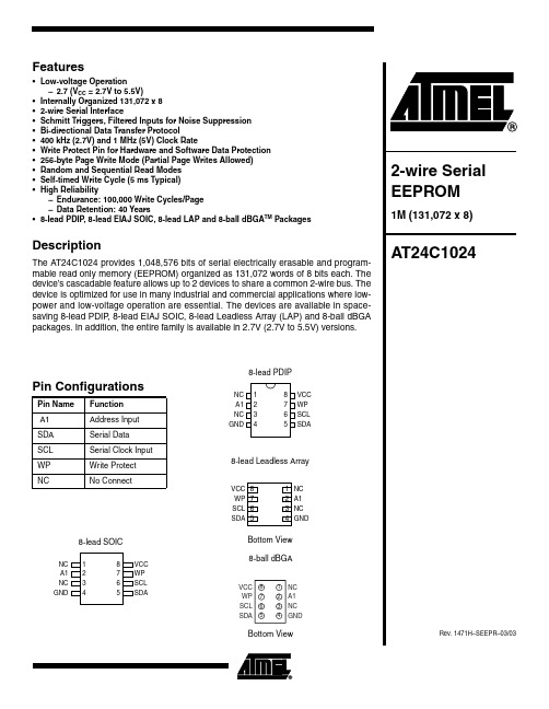
1Features•Low-voltage Operation –2.7 (V CC = 2.7V to 5.5V)•Internally Organized 131,072 x 8•2-wire Serial Interface•Schmitt Triggers, Filtered Inputs for Noise Suppression •Bi-directional Data Transfer Protocol•400 kHz (2.7V) and 1 MHz (5V) Clock Rate•Write Protect Pin for Hardware and Software Data Protection •256-byte Page Write Mode (Partial Page Writes Allowed)•Random and Sequential Read Modes •Self-timed Write Cycle (5 ms Typical)•High Reliability–Endurance: 100,000 Write Cycles/Page –Data Retention: 40 Years•8-lead PDIP , 8-lead EIAJ SOIC, 8-lead LAP and 8-ball dBGA TM PackagesDescriptionThe AT24C1024 provides 1,048,576 bits of serial electrically erasable and program-mable read only memory (EEPROM) organized as 131,072 words of 8 bits each. The device’s cascadable feature allows up to 2 devices to share a common 2-wire bus. The device is optimized for use in many industrial and commercial applications where low-power and low-voltage operation are essential. The devices are available in space-saving 8-lead PDIP, 8-lead EIAJ SOIC, 8-lead Leadless Array (LAP) and 8-ball dBGA packages. In addition, the entire family is available in 2.7V (2.7V to 5.5V) versions.Pin ConfigurationsPin Name Function A1Address Input SDA Serial Data SCL Serial Clock Input WPWrite Protect NCNo Connect8-lead PDIP8-lead Leadless ArrayBottom View8-lead SOIC8-ball dBGABottom View2AT24C10241471H–SEEPR–03/03Block DiagramAbsolute Maximum Ratings*Operating Temperature..................................-55°C to +125°C *NOTICE:Stresses beyond those listed under “Absolute Maximum Ratings” may cause permanent dam-age to the device. This is a stress rating only and functional operation of the device at these or any other conditions beyond those indicated in the operational sections of this specification is not implied. Exposure to absolute maximum rating conditions for extended periods may affect device reliability.Storage Temperature.....................................-65°C to +150°C Voltage on Any Pinwith Respect to Ground.....................................-1.0V to +7.0V Maximum Operating Voltage ..........................................6.25V DC Output Current........................................................5.0 mA3AT24C10241471H–SEEPR–03/03Pin DescriptionSERIAL CLOCK (SCL): The SCL input is used to positive edge clock data into each EEPROM device and negative edge clock data out of each device.SERIAL DATA (SDA): The SDA pin is bi-directional for serial data transfer. This pin is open-drain driven and may be wire-ORed with any number of other open-drain or open-collector devices.DEVICE/PAGE ADDRESSES (A1): The A1 pin is a device address input that can be hard-wired or left not connected for hardware compatibility with AT24C128/256/512. When the A1pin is hardwired, as many as two 1024K devices may be addressed on a single bus system (device addressing is discussed in detail under the Device Addressing section). When the pin is not hardwired, the default A1 is zero.WRITE PROTECT (WP): The hardware Write Protect pin is useful for protecting the entire contents of the memory from inadvertent write operations. The write-protect input, when tied to GND, allows normal write operations. When WP is tied high to V CC , all write operations to the memory are inhibited. If left unconnected, WP is internally pulled down to GND. Switching WP to V CC prior to a write operation creates a software write-protect function.Memory OrganizationAT24C1024, 1024K SERIAL EEPROM: The 1024K is internally organized as 512 pages of 256 bytes each. Random word addressing requires a 17-bit data word address.4AT24C10241471H–SEEPR–03/03Pin Capacitance (1)Note:1.This parameter is characterized and is not 100% tested.DC CharacteristicsNote:1.V IL min and V IH max are reference only and are not tested.Applicable over recommended operating range from T A = 25°C, f = 1.0 MHz, V CC = +2.7V.Symbol Test ConditionMax Units Conditions C I/O Input/Output Capacitance (SDA)8pF V I/O = 0V C IN Input Capacitance (A 1, SCL)6pFV IN = 0VApplicable over recommended operating range from: T AI = -40°C to +85°C, V CC = +2.7V to +5.5V, T AC = 0°C to +70°C,V CC = +2.7V to +5.5V (unless otherwise noted).Symbol Parameter Test ConditionMin TypMax Units V CC Supply Voltage 2.75.5V I CC Supply Current V CC = 5.0V READ at 400 kHz 2.0mA I CC Supply Current V CC = 5.0V WRITE at 400 kHz 5.0mA I SB Standby Current V CC = 2.7V V IN = V CC or V SS3.0µA V CC = 5.5V 6.0µA I LI Input Leakage Current V IN = V CC or V SS 0.10 3.0µA I LO Output Leakage CurrentV OUT = V CC or V SS0.053.0µA V IL Input Low Level (1)-0.6V CC x 0.3V V IH Input High Level (1)V CC x 0.7V CC + 0.5V V OL Output Low LevelV CC = 3.0VI OL = 2.1 mA0.4V5AT24C10241471H–SEEPR–03/03AC Characteristics2.AC measurement conditions:R L (connects to V CC ): 1.3 k Ω (2.7V , 5V)Input pulse voltages: 0.3 V CC to 0.7 V CC Input rise and fall times: ≤50 nsInput and output timing reference voltages: 0.5 V CCApplicable over recommended operating range from T A = -40°C to +85°C, V CC = +2.7V to +5.5V, C L = 100 pF (unless otherwise noted). Test conditions are listed in Note 2.Symbol ParameterTest Conditions MinMax Units f SCL Clock Frequency, SCL 4.5V ≤ V CC ≤ 5.5V 2.7V ≤ V CC ≤ 5.5V 1000400kHz t LOW Clock Pulse Width Low 4.5V ≤ V CC ≤ 5.5V 2.7V ≤ V CC ≤ 5.5V 0.41.3µs t HIGH Clock Pulse Width High 4.5V ≤ V CC ≤ 5.5V 2.7V ≤ V CC ≤ 5.5V 0.40.6µs t AA Clock Low to Data Out Valid4.5V ≤ V CC ≤5.5V 2.7V ≤ V CC ≤ 5.5V 0.050.050.550.9µs t BUF Time the bus must be free before a new transmission can start (1) 4.5V ≤ V CC ≤ 5.5V 2.7V ≤ V CC ≤ 5.5V 0.51.3µs t HD.STA Start Hold Time 4.5V ≤ V CC ≤ 5.5V 2.7V ≤ V CC ≤ 5.5V 0.250.6µs t SU.STA Start Setup Time 4.5V ≤ V CC ≤ 5.5V 2.7V ≤ V CC ≤ 5.5V0.250.6µs t HD.DAT Data In Hold Time 0µs t SU.DA T Data In Setup Time 100ns t R Inputs Rise Time (1)0.3µs t F Inputs Fall Time (1) 4.5V ≤ V CC ≤ 5.5V 2.7V ≤ V CC ≤ 5.5V 100300ns t SU.STO Stop Setup Time 4.5V ≤ V CC ≤ 5.5V 2.7V ≤ V CC ≤ 5.5V0.250.6µs t DH Data Out Hold Time 50ns t WRWrite Cycle Time10ms Endurance (1) 5.0V , 25°C, Page Mode100KWrite Cycles6AT24C10241471H–SEEPR–03/03Device OperationCLOCK and DATA TRANSITIONS: The SDA pin is normally pulled high with an external device. Data on the SDA pin may change only during SCL low time periods (refer to Data Validity timing diagram). Data changes during SCL high periods will indicate a start or stop condition as defined below.START CONDITION: A high-to-low transition of SDA with SCL high is a start condition which must precede any other command (refer to Start and Stop Definition timing diagram).STOP CONDITION: A low-to-high transition of SDA with SCL high is a stop condition. After a read sequence, the Stop command will place the EEPROM in a standby power mode (refer to Start and Stop Definition timing diagram).ACKNOWLEDGE: All addresses and data words are serially transmitted to and from the EEPROM in 8-bit words. The EEPROM sends a zero during the ninth clock cycle to acknowl-edge that it has received each word.STANDBY MODE: The AT24C1024 features a low-power standby mode which is enabled: a)upon power-up and b)after the receipt of the STOP bit and the completion of any internal operations.MEMORY RESET: After an interruption in protocol, power loss or system reset, any 2-wire part can be reset by following these steps:1.Clock up to 9 cycles,2.Look for SDA high in each cycle while SCL is high.3.Create a start condition.7AT24C10241471H–SEEPR–03/03Bus Timing (SCL: Serial Clock, SDA: Serial Data I/O)Write Cycle Timing (SCL: Serial Clock, SDA: Serial Data I/O)Note:1.The write cycle time t WRis the time from a valid stop condition of a write sequence to the end of the internal clear/write cycle.8AT24C10241471H–SEEPR–03/03Data ValidityStart and Stop DefinitionOutput Acknowledge9AT24C10241471H–SEEPR–03/03DeviceAddressingThe 1024K EEPROM requires an 8-bit device address word following a start condition to enable the chip for a read or write operation (refer to Figure 1). The device address word con-sists of a mandatory one, zero sequence for the first five most significant bits as shown. This is common to all 2-wire EEPROM devices.The 1024K uses the one device address bit, A1, to allow up to two devices on the same bus.The A1 bit must compare to the corresponding hardwired input pin. The A1 pin uses an inter-nal proprietary circuit that biases it to a logic low condition if the pin is allowed to float.The seventh bit (P 0) of the device address is a memory page address bit. This memory page address bit is the most significant bit of the data word address that follows. The eighth bit of the device address is the read/write operation select bit. A read operation is initiated if this bit is high and a write operation is initiated if this bit is low.Upon a compare of the device address, the EEPROM will output a zero. If a compare is not made, the device will return to a standby state.DATA SECURITY: The AT24C1024 has a hardware data protection scheme that allows the user to write-protect the entire memory when the WP pin is at V CC .WriteOperationsBYTE WRITE: To select a data word in the 1024K memory requires a 17-bit word address.The word address field consists of the P 0 bit of the device address, then the most significant word address followed by the least significant word address (refer to Figure 2)A write operation requires the P 0 bit and two 8-bit data word addresses following the device address word and acknowledgment. Upon receipt of this address, the EEPROM will again respond with a zero and then clock in the first 8-bit data word. Following receipt of the 8-bit data word, the EEPROM will output a zero. The addressing device, such as a microcontroller,then must terminate the write sequence with a stop condition. At this time the EEPROM enters an internally timed write cycle, T WR , to the nonvolatile memory. All inputs are disabled during this write cycle and the EEPROM will not respond until the write is complete (refer to Figure 2).PAGE WRITE: The 1024K EEPROM is capable of 256-byte page writes.A page write is initiated the same way as a byte write, but the microcontroller does not send a stop condition after the first data word is clocked in. Instead, after the EEPROM acknowledges receipt of the first data word, the microcontroller can transmit up to 255 more data words. The EEPROM will respond with a zero after each data word received. The microcontroller must ter-minate the page write sequence with a stop condition (refer to Figure 3).The data word address lower 8 bits are internally incremented following the receipt of each data word. The higher data word address bits are not incremented, retaining the memory page row location. When the word address, internally generated, reaches the page boundary, the following byte is placed at the beginning of the same page. If more than 256 data words are transmitted to the EEPROM, the data word address will “roll over” and previous data will be overwritten. The address “rollover” during write is from the last byte of the current page to the first byte of the same page.ACKNOWLEDGE POLLING: Once the internally timed write cycle has started and the EEPROM inputs are disabled, acknowledge polling can be initiated. This involves sending a start condition followed by the device address word. The read/write bit is representative of the operation desired. Only if the internal write cycle has completed will the EEPROM respond with a zero, allowing the read or write sequence to continue.10AT24C10241471H–SEEPR–03/03ReadOperationsRead operations are initiated the same way as write operations with the exception that the read/write select bit in the device address word is set to one. There are three read operations:current address read, random address read and sequential read.CURRENT ADDRESS READ: The internal data word address counter maintains the last address accessed during the last read or write operation, incremented by one. This address stays valid between operations as long as the chip power is maintained. The address “rollover”during read is from the last byte of the last memory page, to the first byte of the first page.Once the device address with the read/write select bit set to one is clocked in and acknowl-edged by the EEPROM, the current address data word is serially clocked out. The microcontroller does not respond with an input zero but does generate a following stop condi-tion (refer to Figure 4).RANDOM READ: A random read requires a “dummy” byte write sequence to load in the data word address. Once the device address word and data word address are clocked in and acknowledged by the EEPROM, the microcontroller must generate another start condition.The microcontroller now initiates a current address read by sending a device address with the read/write select bit high. The EEPROM acknowledges the device address and serially clocks out the data word. The microcontroller does not respond with a zero but does generate a fol-lowing stop condition (refer to Figure 5).SEQUENTIAL READ: Sequential reads are initiated by either a current address read or a ran-dom address read. After the microcontroller receives a data word, it responds with an acknowledge. As long as the EEPROM receives an acknowledge, it will continue to increment the data word address and serially clock out sequential data words. When the memory address limit is reached, the data word address will “roll over” and the sequential read will con-tinue. The sequential read operation is terminated when the microcontroller does not respond with a zero, but does generate a following stop condition (refer to Figure 6).11AT24C10241471H–SEEPR–03/03Figure 1. Device AddressFigure 2. Byte WriteFigure 3. Page WriteFigure 4.Current Address Read12AT24C10241471H–SEEPR–03/03Figure 5. Random ReadFigure 6.Sequential Read13AT24C10241471H–SEEPR–03/03Note:For 2.7V devices used in the 4.5V to 5.5V range, please refer to performance values in the AC and DC Characteristics tables.Ordering InformationOrdering CodePackage Operation RangeA T24C1024-10CI-2.7A T24C1024C1-10CI-2.7A T24C1024-10PI-2.7A T24C1024W-10SI-2.7A T24C1024-10UI-2.78CN38CN18P38S28U8Industrial (-40°C to 85°C)Package Type8CN38-lead, 0.230" Wide, Leadless Array Package (LAP)8CN18-lead, 0.300" Wide, Leadless Array Package (LAP)8P38-lead, 0.300" Wide, Plastic Dual In-line Package (PDIP)8S28-lead, 0.200" Wide, Plastic Gull Wing Small Outline Package (EIAJ SOIC)8U88-ball, die Ball Grid Array Package (dBGA)Options-2.7Low Voltage (2.7V to 5.5V)14AT24C10241471H–SEEPR–03/03Packaging Information8CN3 – LAP15AT24C10241471H–SEEPR–03/038CN1 – LAP16AT24C10241471H–SEEPR–03/038P3 – PDIP17AT24C10241471H–SEEPR–03/038S2 – EIAJ SOIC18AT24C10241471H–SEEPR–03/038U8 – dBGA1471H–SEEPR–03/03xMDisclaimer: Atmel Corporation makes no warranty for the use of its products, other than those expressly contained in the Company’s standard warranty which is detailed in Atmel’s Terms and Conditions located on the Company’s web site. The Company assumes no responsibility for any errors which may appear in this document, reserves the right to change devices or specifications detailed herein at any time without notice, and does not make any commitment to update the information contained herein. No licenses to patents or other intellectual property of Atmel are granted by the Company in connection with the sale of Atmel products, expressly or by implication. Atmel’s products are not authorized for use as critical components in life support devices or systems.Atmel CorporationAtmel Operations2325 Orchard Parkway San Jose, CA 95131Tel: 1(408) 441-0311Fax: 1(408) 487-2600Regional HeadquartersEuropeAtmel SarlRoute des Arsenaux 41Case Postale 80CH-1705 Fribourg SwitzerlandTel: (41) 26-426-5555Fax: (41) 26-426-5500AsiaRoom 1219Chinachem Golden Plaza 77 Mody Road Tsimshatsui East Kowloon Hong KongTel: (852) 2721-9778Fax: (852) 2722-1369Japan9F, Tonetsu Shinkawa Bldg.1-24-8 ShinkawaChuo-ku, Tokyo 104-0033JapanTel: (81) 3-3523-3551Fax: (81) 3-3523-7581Memory2325 Orchard Parkway San Jose, CA 95131Tel: 1(408) 441-0311Fax: 1(408) 436-4314Microcontrollers2325 Orchard Parkway San Jose, CA 95131Tel: 1(408) 441-0311Fax: 1(408) 436-4314La Chantrerie BP 7060244306 Nantes Cedex 3, France Tel: (33) 2-40-18-18-18Fax: (33) 2-40-18-19-60ASIC/ASSP/Smart CardsZone Industrielle13106 Rousset Cedex, France Tel: (33) 4-42-53-60-00Fax: (33) 4-42-53-60-011150 East Cheyenne Mtn. Blvd.Colorado Springs, CO 80906Tel: 1(719) 576-3300Fax: 1(719) 540-1759Scottish Enterprise Technology Park Maxwell BuildingEast Kilbride G75 0QR, Scotland Tel: (44) 1355-803-000Fax: (44) 1355-242-743RF/AutomotiveTheresienstrasse 2Postfach 353574025 Heilbronn, Germany Tel: (49) 71-31-67-0Fax: (49) 71-31-67-23401150 East Cheyenne Mtn. Blvd.Colorado Springs, CO 80906Tel: 1(719) 576-3300Fax: 1(719) 540-1759Biometrics/Imaging/Hi-Rel MPU/High Speed Converters/RF DatacomAvenue de Rochepleine BP 12338521 Saint-Egreve Cedex, France Tel: (33) 4-76-58-30-00Fax: (33) 4-76-58-34-80e-mailliterature@Web Site© Atmel Corporation 2003. All rights reserved. Atmel ® and combinations thereof, are the registered trademarks, and dBG A ™ is the trademark of Atmel Corporation or its subsidiaries. Other terms and product names may be the trademarks of others.。

AT24C01A/02/04/08A/16A提供1024/2048/4096/8192/16384个连续的可擦除的位,以及由每8位组成一个字节的可编程只读存储器(EEPROM),其分别提供128/256/512/1024/2048个字节。
该设备适用在许多低功耗和低电压操作的工业和商业应用中。
1引脚描述1.1串行时钟(SCL)SCL输入用于正向输出边缘时钟信号到每个EEPROM设备,以及每个设备输出的反向边缘时钟数据。
1.2串行数据(SDA)SDA引脚是用于串行数据双向传输。
该引脚为开漏输出,同时可以与其他开漏极或集电极开路器件进行线或。
1.3设备/页地址(A2,A1,A0)对于AT24C01A和AT24C02,A2、A1和A0引脚是配置器件的硬件地址输入。
一根总线上可以连接多达八个1K / 2K的设备(器件寻址部分详细讨论了器件寻址)。
AT24C04使用A2和A1引脚作为硬件地址输入,在一根总线上有4个4K 的设备可用来寻址。
A0引脚没有连接。
AT24C08A只使用A2引脚作为硬件地址输入,在一根总线上有2个8K 的设备可用来寻址。
A0和A1引脚没有连接。
AT24C16A不使用设备地址引脚,这限制了一根总线上只能挂一个设备。
A0、A1和A2引脚没有连接。
1.4写保护(WP)AT24C01A / 02 / 04 / 08A/ 16A有一个写保护引脚,提供硬件数据保护。
写保护引脚允许正常读/写操作时连接到GND。
当写保护引脚连接到VCC,写保护功能启用和操作如下表所示。
2设备操作2.1时钟和数据转换SDA引脚通常情况下拉高。
SDA引脚上的数据只能在SCL低时间段内更改,而启动条件或停止条件在SCL为高时进行。
2.2启动条件在任何其他指令之前,SDA由高变为低,且SCL为高。
2.3停止条件SDA由低变为高,且SCL为高。
在读取序列之后,执行停止命令后EEPROM进入备用电源模式。
2.4应答所有地址和数据字都是从EEPROM串行发送和接收8位字节。
AT24C1024介绍AT24C10242 线串⾏EEPROM特性低电压操作:2.7(Vcc=2.7V to 5.5V)内部组织:131,072*8 位=1M2 线串⾏接⼝施密特触发器,噪声抑制滤波输⼊双向数据传输协议时钟速率:400kHz(2.7V)和1MHz(5V) 硬件写保护引脚和软件数据保护256 字节页写模式(允许部分页⾯写⼊)随机和顺序读写模式⾃定义写周期(5ms)⾼可靠性:耐久⼒:写周期/页100,000 次数据保留:40 年8 引脚PDIP,8 引脚有铅SOIC 封装,8 引脚⽆铅阵列和8 引脚球状dBGA 封装描述AT24C1024 提供1,048,567 位的串⾏可电擦除和可编程只读存储器(EEPROM),它的每8 位组成⼀个字节,共131,072 个字节。
该设备的级联功能允许多达2 个设备共亨同⼀条2- 线总线。
该设备适合⽤于许多⼯业和商业,应⽤必要的低功耗和低电压的操作。
该器件可提供节省空间的8 引脚PDIP,8 引脚有铅SOIC 封装,8 引脚⽆铅阵列和8 引脚球状dBGA 封装。
另外,这⼀系列产品允许在2.7V(2.7V~5.5V)下⼯作。
绝对最⼤额定值:⼯作温度:-55~+125存储温度:-65~+150任何引脚的对地电压:-1.0V~+7.0V最⼤⼯作电压:6.25V 直流输出电流:5.0mA注意:强制⾼出“绝对最⼤额定值”可能导致设备的永久损坏。
设备的压⼒等级和功能操作只有在这些或超出本规范所标明的其他任何条件下是不允许的。
长时间⼯作在绝对最⼤额定值的条件下可能影响设备的可靠性。
引脚描述:串⾏时钟(SCL):SCL 的输⼊是在时钟的上升沿数据进⼊每个EEPROM 设备和下降沿数据输出每个设备。
串⾏数据(SDA):SDA 引脚是双向串⾏数据传输的。
这个引脚是漏极输出的,可以与其它的漏极开路或集电极开路的设备线或。
器件/ 页地址(A1 ):A1 引脚是设备的输⼊地址,它能够通过导线与不兼容的设备AT24C128/256/512 连接。
CA T24C 161/162(16K),CAT24C081 /082(8K) CAT24C041/042(4K),CAT24C021/022(2K)I2C串行CMOS E2PROM,精确的复位控制器和看门狗定时器控制电路特性•数据线上的看门狗定时器(仅对CA T24Cxxl)籲可编程复位门槛电平籲高数据传送速率为400KHz和I2C总线兼容• 2.7V至6V的工作电压•低功耗CMOS工艺籲16字节页写缓冲区籲片内防误擦除写保护籲高低电平复位信号输出——精确的电源电压监视器——可选择5V、3.3V和3V的复位门槛电平•100万次擦写周期•数据保存可长达100年•8脚DIP或SOIC封装•商业级、工业级和汽车温度范围概述CA T24Cxxx是集E2PROM存储器,复位微控制器和看门狗定时器三种流行功能与一体的芯片。
CAT24C161/162 (16K),CAT24C081/082 (8K),CA T24C041/042 (4K)和CAT24C021/022 (2K)以I2C是串行CMOS E2PROM器件。
釆用CMOS工艺大降低了器件的功耗。
CA T24Cxxx 另一特点是16字节的页写缓冲区,提供8脚DIP和SOIC 封装。
CA T24Cxxx的复位功能和看门狗定时器功能保证系统出现故障的时候能给CPU —个复位信号。
CA T24Cxxx 的2脚输出低电平复位信号,7脚输出高电平复位信号。
CAT24Cxxl看狗溢出信号从SDA脚输出。
CAT24Cxx2不具备看门狗功能。
绝对最大参数工作温度:-55°C〜125°C贮存温度:-65°C〜15°C各管脚承受对地电压:-2.0V〜Vcc+2.0V VCC对地电压范围:-2.0V〜7.0V 最大功耗: 1.0W管脚焊接温度(10S): 300 °C输出短路电流:100mA管脚配置]V C C ]RESET方框图表一直流操作特性表二上电时序管脚介绍WP:写保护将该管脚接Vcc,E2PRON就实现写保护(只读)。
AT24Cxx芯片读写--IIC总线AT24Cxx芯⽚读写--IIC总线型号容量器件寻址字节(8位) ⽚次装载字节数AT24C01 128×8 1010A2A1A0 R/W 8AT24C02 256×8 1010A2A1A0 R/W 8AT24C04 512×8 1010A2A1P0 R/W 16AT24C08 1024×8 1010A2P1P0 R/W 16AT24C16 2048×8 1010P2P1P0 R/W 16AT24C32 4096*8 1010A2A1A0 R/W 32AT24C64 8192*8 1010A2A1A0 R/W 32AT24C128 16384*8 1010A2A1A0 R/W 64AT24C256 16384*8 1010A2A1A0 R/W 64AT24C系列 E2PROM接⽚及地址选择设备地址:24xx系列的可以通过修改外的地址引脚来设置不同的地址.IIC地址的确定,AT24C系列的,24c01,02 1K/2K EEPROM 在⽚条IIC总线上可以挂8个,地址由A2,A1,A0确定;24C04 4k EEPROM 只有A2,A1的做地址位,这样⽚条IIC总线上能挂4个设备,A0是⽚来确定内部页地址的,A0在芯⽚上没有线连接的(NA); 24C08, 8k EEPROM 使⽚A2来确定地址线,A1,A0位是在确定内部页地址的,⽚条IIC总线能扩展2⽚; 24C16 16k,A2A1A0都是确定内部页地址的;⽚条总线上只能挂1个⽚个这样的设备.但在AT24C32 ,24C64中⽚有改变,32,64中发送的内部地址都是发2次,⽚地址和低地址,这样有16位地址位可以确定内部地址,就不需要⽚A2A1A0来确定地址了.控制器的读写时序AT24C01---AT24C16读: 发设备地址---> 送8位地址---->发设备地址--->读取--->NOACK--->停⽚;写:发设备地址--->送8位地址----->写数据--->停⽚;AT24C32.AT24C64读:发设备地址--->送⽚8位地址--->送低8位地址--->发设备地址--->读取----->NOACK--->停⽚写:发设备地址--->送⽚8位地址----->送低8位地址---->写数据--->停⽚;。