Adaptive Checkpointing with Storage Management for Mobile Environments
- 格式:pdf
- 大小:248.05 KB
- 文档页数:27

[公司名称]nRF5 SDK 中文翻译——寻向功能篇[作者姓名]2022-4-29修订历史目录..目录 (1)第1章驱动支持列表..............................................................................错误!未定义书签。
第2章Clock 时钟 ..................................................................................错误!未定义书签。
2.1 简介.............................................................................................错误!未定义书签。
2.2 驱动配置.....................................................................................错误!未定义书签。
2.3 控制HFCLK...............................................................................错误!未定义书签。
2.4 控制LFCLK(仅在不带SoftDevice的情况下) ...................错误!未定义书签。
2.5 控制LFCLK的校准(不带软设备并使用RC作为时钟源) .......错误!未定义书签。
第3章COMP (比较器)...........................................................................错误!未定义书签。
3.1 简介.............................................................................................错误!未定义书签。

零维护缓存保护简报降低数据中心运营成本,最大限度保护缓存数据产品要点低运营成本– 没有电池相关的安装、监控、维护、弃置或者更换成本停电情况下不会丢失数据– 取代锂电池零维护缓存保护– 无需监测电池充电情况– 更换电池过程中不需要关闭系统– 无限期地保护数据 -“在电池电量耗尽之前”不需要急于重启系统– 保存数据长达数年之久RAID缓存即时保护– 充电只需要几分钟时间,而不是几小时– 环境优化RAID性能环保– 无毒电池废弃处理– 配合Adaptec智能电源管理功能打造行业“最绿色”解决方案- 遵从简化的 IATA 规则完全集成在5Z系列RAID控制上并作为6系列的附件套件IDC预计,在四年时间内一步IT设备的运营成本将增长到原始采购成本的4倍。
Adaptec 6系列和5Z系列RAID控制卡采用了零维护缓存保护(Zero-Maintenance CacheProtection,ZMCP)功能,最大限度保护缓存数据,大幅削减成本并减少了复杂、杂乱和昂贵的锂电池对环境的影响,同时提高了缓存保护和缓存性能。
为什么你需要缓存保护随着用户持续关注针对快速增加的数据集进行的容量利用率优化,RAID 5和RAID 6在企业级存储系统中的运用继续增长着。
然而,除非启用了所有可用缓存,否则系统无法实现最佳性能。
不过,启用控制卡缓存之后,数据被保存在控制卡的内存中,并有可能在系统断电的情况下丢失。
防止这种情况发生的最常见保护措施就是使用一个直接安装在控制卡上的电池备份单元(BBU)来备份控制卡缓存。
这种电池是维护板载缓存数据,直到恢复对电池备份单元的供电。
电池备份单元的第二个使用方法就是配合Adaptec 6系列、5Z系列、5系列和2系列RAID控制卡产品系列所提供的Adaptec智能电源管理功能(Intelligent Power Management)。
为了让控制卡降低硬盘转速或者完全停转,硬盘中必须是没有任何I/O活动的。

Adaptec ® Product GuideTrusted Storage SolutionsData Center SolutionsThe Microchip name and logo, the Microchip logo, Adaptec and maxCrypto is a trademark are registered trademarks of Microchip Technology Incorporated in the U.S.A. and other countries. All other trademarks mentioned herein are property of their respective companies.© 2020, Microchip Technology Incorporated. All Rights Reserved. 1/20 DS00003375ASupportMicrochip is committed to supporting its customers in developing products faster and more efficiently. We maintain a worldwide network of field applica -tions engineers and technical support ready to provide product and system assistance. For more information, please visit :• Technical Support: /support • Evaluation samples of any Microchip device:/sample • Knowledge base and peer help:/forums• Sales and Global Distribution: /salesTrainingIf additional training interests you, Microchip offers several resources including in-depth technical training and reference material, self-paced tutorials and significant online resources.• Overview of Technical Training Resources: /training • MASTERs Conferences:/masters • Developer Help Website:/developerhelp • Technical Training Centers:/seminarsMicrochip Technology Inc. | 2355 W. Chandler Blvd. | Chandler AZ, 85224-6199Adaptec ® Product GuideEach New Product Family Has Unique, Differentiating FeaturesSmartRAID 3100The SmartRAID 3100 is optimized for Enterprise storage applications that require the highest level of data availability and data center applications that benefit from caching.• Adapters with up to 24 ports using 28 nm SAS/SATA-optimized silicon, offering the industry’s lowest power • Z ero Maintenance Cache Protection (ZMCP) with a cache size up to 4 GB with integrated cache backupcircuitry for optimal cost, thermal performance and operating efficiency • Board options without cache backup• Mixed mode enables drives to be independently configured as raw drives or as part of a logical volume • maxCache 4.0 included on 315x and 316x adapters• maxCrypto controller-based encryption on the 3162-8i/e adapterSmartHBA 2100The SmartHBA 2100 is optimized for Software-Defined Storage (SDS) applications that require hardware RAID for OS boot drives as well as entry-level RAID for SMBs.• The only basic hardware RAID solution offering a fully featured, high-performance Host Bus Adapter(HBA) for drives configured as raw drives, required for multi-path IO and SDS applications • RAID levels 0, 1, 10, 5• Industry’s only basic hardware RAID solution with more than 8 ports• Mixed mode enables drives to be independently configured as raw drives or as part of a logical volumeHBA 1100The HBA 1100 is optimized for SDS, cold storage, and raw high-performance connectivity.• Adapters with up to 24 ports using 28 nm SAS/SATA-optimized silicon, offering the industry’s lowestpower• Support for host-managed and host-aware Shingled Magnetic Recording (SMR) drives • Broad OS driver support, including inbox driver support • Performance of up to 1.7M IOPS Smart Storage Solutions OverviewCablesSmartRAIDSmartRAIDSmartHBASmartRAID 3100 RAID AdaptersAdaptec 12 Gbps SmartRAID 3100 adapters have an 8-lane PCIe ®Gen 3 host bus interface, a SmartROC 3100 processor, an MD2 low-profile form factor, and can be scaled to a maximum of 256 SAS/SATA devices*. The newest addition, the SmartRAID 3162-8i/e, provides the industry’s only data-at-rest controller-based encryption solution, maxCrypto. Supporting operating systems include include Microsoft Windows ®, Red Hat, SUSE, Fedora, Debian, Ubuntu, Sun Solaris, FreeBSD, VMware ESXi, open-source Linux ®drivers and inbox drivers.Series 8 RAID AdaptersAdaptec 12 Gbps RAID Adapters have an 8-lane PCIe Gen3 host bus interface,a 12 Gbps RoC processor, a MD2 low-profile form factor, and can be scaled to a maximum of 256 SAS/SATA devices*. Supporting operating systems include Microsoft Windows, Red Hat Linux, SUSE Linux, Fedora, Debian Linux, Ubuntu Linux,Sun Solaris, FreeBSD and VMware ESXi.SmartHBA and Host Bus Adapters (HBA)Adaptec 12 Gbps HBAs have an 8-lane PCIe Gen 3 host bus interface, a SmartIOC 2100 processor, an MD2 low-profile form factor, and can be scaled to a max -imum of 256 SAS/SATA devices*. In addition, the SmartHBA 2100 series uniquely combines the capabilities of a full-featured HBA, with those of a basic hardware RAID adapter. Supporting operating systems include Microsoft Windows, Red Hat, SuSE, CentOS, Ubuntu, VMware ESXi, FreeBSD, Solaris and Citrix Xen Server.SmartHBA 2100 Host Bus Adaptor Specifications4SAS-SBExternal CablesACK-E-HDmSAS-HDmSASACK-E-HDmSAS-mSASMake the Right Connection With Adaptec 12 Gbps and 6 Gbps SAS HD CablesAdaptec SmartRAID 3100, SmartHBA 2100, HBA 1100 and Series 8/8Q/8E RAID adapters are configured with mini-SAS HD connectors to allow for maximum performance and connectivity in a MD2 low-profile form factor. Pick the right cable for your internal or external storage solution.。

Entrust Adaptive Issuance Instant ID SoftwareHIGHLIGHTSLaunch your ID card program with confidenceEntrust Adaptive Issuance Instant ID software is the ideal starting point for organizations that want to make their people and premises more secure. Built for a single-user environment, InstantID software delivers the core tools you need to easily design, print, and manage ID cards and credentials. This user-friendly software offers you a complete solution for issuing basic IDs. Plus, you can easily scale up to another, more feature-rich edition in the Instant ID software suite as your needs grow.KEY BENEFITSEase of use. Drag-and-drop features make the software intuitive and easyto use, allowing you to spend less time learning and more time creating new credentials.• B rowser-based applications do notrequire an internet connection.• P rovides administrators with anintuitive interface to build the rightworkflows and card design. Everyday users can automatically follow astandardized process to improveaccuracy.• T he Quick Start Wizard gets usersfrom initial login to print with minimal setup and configuration.Configure to meet your needs. Settings can be configured to allow everyday users the ability to capture the data they want, how they want, while ensuring only the proper information is captured. Use your existing data. Import data from CSV and ASCII files or integrate directly with Microsoft Access, SQL Server, or MySQL*.*Available with Instant ID Plus editionEntrust Adaptive Issuance at a glanceEntrust Adaptive Issuance Instant ID offers a basic card issuance edition that’s just right for you – now and into the future.Instant ID Express software includes:• B asic photo capture• Data import• Credential designer• D rag-and-drop workflowsfor a single-user environment• E mbedded database for record storage and retrieval Instant ID Plus software also includes:• S ignature capture• DSLR camera support• Report capabilities• Composite field support• SQL Server support• MySQL support• Microsoft Access support• Batch printingBuild a complete card-issuance solutionEntrust Adaptive Issuance Instant ID software works with Entrust printers, supplies, and global services to give you a complete ID-issuance solution that delivers exceptional results.TECHNICAL SPECIFICATIONS SYSTEM REQUIREMENTSOperating System: Microsoft Windows 7 / 8.1 / 10 Mobile Operating System: iOS, Android, Microsoft Surface Web Browser:Chrome, Internet Explorer v10or 11, EdgeMemory:4 GB (8 GB recommended)Hard Drive:1 GB of computer drive spaceDesktop or PC Screen Resolution:1360 x 768(minimum)INSTANT ID SOFTWARE STANDARD FEATURESCredential Design• F ront and back card design, pre-designed card templates• V ariable/Static text field, photograph field, variable/static graphic field, date field• Magnetic stripe, bar code and QR code Workflow• T ext field, static text field, static graphic field,date field, print count field• A uto-sequence field, check box field, list field• T ext field mask, field option – read only, hidden,mandatory, searchableDatabase & Data Import• I mport data from CSV, ASCII fileLanguage Support• E nglish, French, German, Japanese, JIS Kanji,Portuguese (Brazilian), Simplified Chinese,Spanish• L ocalization utility for other languagesPrinter Support• Instant ID integrates with non-Entrust devicesPhoto Capture• F ile input, TWAIN, DirectShow, web browserABOUT ENTRUST CORPORATIONEntrust secures a rapidly changing world by enabling trusted identities, payments,and data protection. Today more than ever, people demand seamless, secure experiences, whether they’re crossing borders, making a purchase, accessing e-government services, or logging into corporate networks. Entrust offers an unmatched breadth of digital security and credential issuance solutions at the very heart of all these interactions. With more than 2,500 colleagues, a network of global partners, and customers in over 150 countries, it’s no wonder the world’s most entrusted organizations trust us.For more information888.690.2424 +1 952 933 1223 ****************Entrust and the Hexagon logo are trademarks, registered trademarks, and/or service marks of Entrust Corporation in the U.S. and/or other countries. All other brand or product names are the property of their respective owners. Because we are continuously improving our products and services, Entrust Corporation Learn more atU.S. Toll-Free Phone: 888 690 2424 International Phone: +1 952 933 1223。

enableexternalizedcheckpoints替代方法-回复替代enableexternalizedcheckpoints 的方法引言:在大数据和分布式计算环境下,容错性和数据一致性是至关重要的。
为了实现这些目标,一种常用的技术是使用检查点机制,即将当前系统状态保存到可靠的存储介质中,以备系统故障时进行恢复。
在某些大规模分布式计算框架中,如Apache Flink,enableexternalizedcheckpoints是一种常用的配置选项,用于启用外部化检查点。
然而,有时候我们可能需要找到替代enableexternalizedcheckpoints 的方法,本文将逐步探讨几种替代方法。
一、checkpoint to local disk(将检查点保存在本地磁盘)先来看一种简单且常见的替代方法,即将检查点保存在本地磁盘。
这种方法的优点是简单直接,不需要额外的外部存储设备。
同时,保存在本地磁盘的检查点可以快速读取,无需网络传输。
然而,缺点也很明显,如果节点出现故障,本地磁盘上的检查点可能无法访问,导致系统恢复失败。
因此,这种方法适用于对数据一致性要求不高,且系统恢复时间要求较短的场景。
二、checkpoint to distributed file system(将检查点保存在分布式文件系统)另一种替代方法是将检查点保存在分布式文件系统中,如Hadoop HDFS 或Apache HBase。
这种方法可以解决本地磁盘故障带来的风险,因为分布式文件系统通常具有备份和容错机制。
同时,分布式文件系统具有高可扩展性和高性能的特点,可以适应大规模分布式计算。
然而,保存在分布式文件系统中的检查点需要通过网络传输,可能会引入一定的延迟。
此外,分布式文件系统的部署和维护可能会增加系统的复杂性和成本。
三、incremental checkpoints(增量检查点)增量检查点是一种优化技术,可以减少检查点的存储和传输成本。

CHIP COILS (CHIP INDUCTORS) LQW03AW□□□□00□ REFERENCE SPECIFICATION1. ScopeThis reference specification applies to chip coils (chip inductors) LQW03AW_00 series for general electronic equipment.2. Part Numbering(Ex.)LQ W 03 A W 5N4 J 0 0 DProductID Structure Dimension(L × W)ApplicationandcharacteristicCategory Inductance Tolerance Performance ElectrodespecificationPackagingD: taping*B: bulk*B: Bulk packing is also available (taping condition: however, products without reels are put in plastic bags).3. Part Number and RatingOperating temperature range -55°C to +125°C (including self-generated heat)Storage temperature range -55°C to +125°CCustomer Part numberMurataPart numberInductance Q(900 MHz)(Typicalvalue)DCresistance(Ω max.)Self-resonantfrequency(GHz min.)Ratedcurrent(mA) Nominalvalue(nH)ToleranceLQW03AW1N0C00D1.0C:±0.2nH 48 0.03 19.0 900 LQW03AW1N1C00D1.1C:±0.2nH 41 0.06 19.0 660 LQW03AW1N7C00D1.7C:±0.2nH 41 0.07 19.0 600 LQW03AW1N8C00D1.8C:±0.2nH 37 0.10 19.0 520 LQW03AW1N9C00D1.9C:±0.2nH 41 0.08 19.0 620 LQW03AW2N0C00D2.0C:±0.2nH 42 0.10 19.0 490 LQW03AW2N1C00D2.1C:±0.2nH 35 0.16 19.0 400 LQW03AW2N2C00D2.2C:±0.2nH 33 0.16 19.0 400 LQW03AW2N7C00D2.7C:±0.2nH 46 0.06 15.0 720 LQW03AW2N8C00D2.8C:±0.2nH 44 0.08 14.0 600 LQW03AW2N9C00D2.9C:±0.2nH 41 0.10 13.0 540 LQW03AW3N0C00D3.0C:±0.2nH 34 0.22 14.0 350 LQW03AW3N1C00D3.1C:±0.2nH 48 0.07 12.0 720 LQW03AW3N2C00D3.2C:±0.2nH 48 0.08 10.0 580 LQW03AW3N3C00D3.3C:±0.2nH 47 0.11 11.0 520 LQW03AW3N4C00D3.4C:±0.2nH 43 0.15 11.0 440 LQW03AW3N5C00D3.5C:±0.2nH 43 0.15 12.0 440 LQW03AW3N6C00D3.6C:±0.2nH 36 0.23 11.0 340 LQW03AW3N7C00D3.7C:±0.2nH 38 0.23 11.0 340 LQW03AW3N9C00D3.9C:±0.2nH 48 0.07 11.0 650 LQW03AW4N3J00D4.3 J:±5% 45 0.12 11.0 480 LQW03AW4N7J00D4.7 J:±5% 45 0.09 9.5 620 LQW03AW5N1J00D5.1 J:±5% 45 0.14 9.5 480 LQW03AW5N4J00D5.4 J:±5% 46 0.21 9.5 420 LQW03AW5N6J00D5.6 J:±5% 37 0.33 8.3 330 LQW03AW5N8J00D5.8 J:±5% 47 0.16 8.8 460 LQW03AW6N2J00D6.2 J:±5% 39 0.22 9.9 360 LQW03AW6N8J00D6.8 J:±5% 42 0.18 7.7 460 LQW03AW7N5J00D7.5 J:±5% 41 0.24 7.5 400 LQW03AW8N2J00D8.2 J:±5% 40 0.26 8.5 290Customer Part numberMurataPart numberInductance Q(900 MHz)(Typicalvalue)DCresistance(Ω max.)Self-resonantfrequency(GHz min.)Ratedcurrent(mA)Nominalvalue(nH)ToleranceLQW03AW8N7J00D8.7J:±5% 39 0.42 7.5 290 LQW03AW9N1J00D9.1J:±5% 46 0.22 6.4 460 LQW03AW10NJ00D10.0J:±5% 37 0.46 7.2 250 LQW03AW11NJ00D11.0J:±5% 37 0.47 7.0 260 LQW03AW12NJ00D12.5J:±5% 39 0.54 6.0 280 LQW03AW13NJ00D13.0J:±5% 39 0.54 5.9 280 LQW03AW14NJ00D13.5J:±5% 37 0.53 6.0 240 LQW03AW15NJ00D15.5J:±5% 38 0.60 5.7 230 4. Testing ConditionsUnless otherwise specified Temperature: ordinary temperature (15°C to 35°C)Humidity: ordinary humidity [25% to 85% (RH)]In case of doubt Temperature: 20°C±2°CHumidity: 60% to 70% (RH)Atmospheric pressure: 86 kPa to 106 kPa5. Appearance and DimensionsUnit mass (typical value): 0.23 mg6. MarkingNo marking.7. Electrical PerformanceNo.ItemSpecificationTest method7.1 InductanceMeet chapter 3 ratings.Measuring equipment: Keysight E4991A or the equivalentMeasuring frequency: Inductance 250 MHz 1.0 nH to 3.9 nH 100 MHz 4.3 nH to 15.5 nH Measuring conditions:Measurement signal level: Approx. 0 dBm Measurement terminal distance: 0.3 mm Electrical length: 10.0 mmMeasuring fixture: Keysight 16197APosition the chip coil under test as shown in the measuring example below and connect it to the electrode by applying weight. Measurement example:Measuring method: see "Electrical performance: Measuring method for inductance/Q" in the chapter"16. Appendix".7.2 QMeet chapter 3 ratings.7.3 DC resistance Meet chapter 3 ratings. Measuring equipment: digital multimeter 7.4 Self-resonantfrequency Meet chapter 3 ratings.Measuring equipment: Keysight N5230A or theequivalent7.5 Rated currentProduct temperature rise: 20°C max.Apply the rated current specified in chapter 3.8. Mechanical PerformanceNo.ItemSpecificationTest method8.1 Bending testNo significant mechanical damage or no sign of electrode peeling off shall be observed. Test substrate: glass-epoxy substrate (100 mm × 40 mm × 0.8 mm) Pressurizing speed: 1 mm/sDeflection: 2 mm Holding time: 5 s8.2 VibrationAppearance shall have no significant mechanical damage.Oscillation frequency: 10 Hz to 55 Hz to 10 Hz, for approx. 1 minTotal amplitude: 1.5 mmTest time: 3 directions perpendicular to each other, 2 h for each direction (6 h in total)No.ItemSpecificationTest method8.3 Solderability90% or more of the outer electrode shall be covered with new solder seamlessly. Flux: immersed in ethanol solution [including anactivator with a chlorine conversion value of 0.06(wt)%]with a rosin content of 25(wt)% for 5 s to 10 s. Solder: Sn-3.0Ag-0.5Cu solderPre-heating: 150°C±10°C/60 s to 90 s Solder temperature: 240°C±5°C Immersion time: 4 s±1 s 8.4 Resistance tosoldering heatAppearance: No significant mechanical damage shall be observed.Inductance change rate: within ±5%Flux: immersed in ethanol solution [including anactivator with a chlorine conversion value of 0.06(wt)%] with a rosin content of 25(wt)% for 5 s to 10 s. Solder: Sn-3.0Ag-0.5Cu solderPre-heating: 150°C±10°C/60 s to 90 s Solder temperature: 270°C±5°C Immersion time: 5 s±1 sPost-treatment: left at a room condition for 24 h±2 h9. Environmental PerformanceThe product is soldered on a substrate for test. No. Item Specification Test method9.1 Heat resistanceAppearance: No significant mechanicaldamage shall be observed.Inductance change rate: within ±5%Q change rate: within ±20%Temperature: 125°C±2°CTest time: 1000 h (+48 h, -0 h)Post-treatment: left at a room condition for 24 h±2 h 9.2 Cold resistanceAppearance: No significant mechanical damage shall be observed.Inductance change rate: within ±5% Q change rate: within ±20%Temperature: -55°C±2°CTest time: 1000 h (+48 h, -0 h)Post-treatment: left at a room condition for 24 h±2 h9.3 HumidityAppearance: No significant mechanical damage shall be observed.Inductance change rate: within ±5% Q change rate: within ±20%Temperature: 70°C±2°CHumidity: 90% (RH) to 95% (RH) Test time: 1000 h (+48 h, -0 h)Post-treatment: left at a room condition for 24 h±2 h 9.4 Temperature cycle Appearance: No significant mechanicaldamage shall be observed.Inductance change rate: within ±5% Q change rate: within ±20%Single cycle conditions:Step 1: -55°C±2°C/30 min±3 minStep 2: ordinary temperature/10 min to 15 min Step 3: +125°C±2°C/30 min±3 minStep 4: ordinary temperature/10 min to 15 min Number of testing: 10 cyclesPost-treatment: left at a room condition for 24 h±2 h10. Specification of Packaging10.1 Appearance and dimensions of tape (8 mm width/paper tape)A (0.52)B (0.65) t 0.75 max.(in mm)10.2 Taping specificationsPacking quantity (Standard quantity) 10000 pcs/reelPacking method The products are placed in embossed cavities of a base tape and sealed by a cover tape.Feed hole position The feed holes on the base tape are on the right side when the cover tape is pulled toward the user. JointThe base tape and the cover tape are seamless.Number of missing productsNumber of missing products within 0.025% of the number per reel or 1 pc., whichever is greater, and are not continuous. The specified quantity per reel is kept.10.3 Break down force of tapeBreak down force of cover tape5 N min.10.4 Peeling off force of cover tapeSpeed of peeling off 300 mm/minPeeling off force0.1 N to 0.6 N (The lower limit is for typical value.)10.5 Dimensions of leader section, trailer section and reelA vacant section is provided in the leader (start) section and trailer (end) section of the tape for the product. The leader section is further provided with an area consisting only of the cover tape (or top tape). (See the diagram below.)10.6 Marking for reelCustomer part number, Murata part number, inspection number (*1), RoHS marking (*2), quantity, etc. *1 Expression of inspection No.: □□ ○○○○(1) (2) (3)(1) Factory code(2) Date First digit: year/last digit of yearSecond digit: month/Jan. to Sep.→1 to 9, Oct. to Dec.→O, N, D Third, Fourth digit: day (3) Serial No.*2 Expression of RoHS marking: ROHS- Y ( ) (1) (2)(1) RoHS regulation conformity(2) Murata classification number10.7 Marking on outer box (corrugated box)Customer name, purchasing order number, customer part number, Murata part number, RoHS marking (*2), quantity, etc.FCover tapetape165°to 180゜10.8 Specification of outer boxDimensions of outer box(mm) Standard reel quantity in outer box (reel)WDH186 186 935* Above outer box size is typical. It depends on a quantity of an order.11. Caution11.1 Restricted applicationsPlease contact us before using our products for the applications listed below which require especially high reliability for the prevention of defects which might directly cause damage to the third party's life, body or property. (1) Aircraft equipment (2) Aerospace equipment (3) Undersea equipment (4) Power plant controlequipment(5) Medical equipment (6) Transportation equipment (vehicles, trains, ships, etc.) (7) Traffic signal equipment (8) Disaster/crimeprevention equipment(9) Data-processing equipment (10) Applications of similar complexity and/or reliability requirements to the applications listed in the above11.2 Precautions on ratingAvoid using in exceeded the rated temperature range, rated voltage, or rated current.Usage when the ratings are exceeded could lead to wire breakage, burning, or other serious fault.11.3 Inrush currentIf an inrush current (or pulse current or rush current) that significantly exceeds the rated current is applied to the product, overheating could occur, resulting in wire breakage, burning, or other serious fault.11.4 Corrosive gasPlease refrain from use since contact with environments with corrosive gases (sulfur gas [hydrogen sulfide, sulfur dioxide, etc.], chlorine, ammonia, etc.) or oils (cutting oil, silicone oil, etc.) that have come into contact with the previously stated corrosive gas environment will result in deterioration of product quality or an open from deterioration due to corrosion of product electrode, etc. We will not bear any responsibility for use under these environments.12. Precautions for UseThis product is for use only with reflow soldering. It is designed to be mounted by soldering. If you want to use other mounting method, for example, using a conductive adhesive, please consult us beforehand.Also, if repeatedly subjected to temperature cycles or other thermal stress, due to the difference in the coefficient of thermal expansion with the mounting substrate, the solder (solder fillet part) in the mounting part may crack.The occurrence of cracks due to thermal stress is affected by the size of the land where mounted, the solder volume, and the heat dissipation of the mounting substrate. Carefully design it when a large change in ambient temperature is assumed.12.1 Land dimensionsThe following diagram shows the recommended land dimensions for reflow soldering.The land dimensions are designed in consideration of electrical characteristics and mountability. Use of other landdimensions may preclude achievement of performance. In some cases, it may result in poor solderability, including positional shift. If you use other land pattern, consider it adequately.a 0.23b 0.65c 0.4(in mm)WDLabelH12.2 Flux and solder usedFlux• Use a rosin-based flux that includes an activator with a chlorine conversion value of 0.06(wt)% to 0.1(wt)%. • Do not use a highly acidic flux with a halide content exceeding 0.2(wt)% (chlorine conversion value). • Do not use a water-soluble flux.Solder• Use Sn-3.0Ag-0.5Cu solder.• Standard thickness of solder paste: 80 μm to 100 μmIf you want to use a flux other than the above, please consult our technical department.12.3 Soldering conditions (reflow)• Pre-heating should be in such a way that the temperature difference between solder and product surface is limited to 150°C max.Cooling into solvent after soldering also should be in such a way that the temperature difference is limited to 100°C max. Insufficient pre-heating may cause cracks on the product, resulting in the deterioration of product quality. • Standard soldering profile and the limit soldering profile is as follows.The excessive limit soldering conditions may cause leaching of the electrode and/or resulting in the deterioration of product quality.Standard profile Limit profilePre-heating 150°C to 180°C/90 s±30 s 150°C to 180°C/90 s±30 s HeatingAbove 220°C/30 s to 60 sAbove 230°C/60 s max.Peak temperature 245°C±3°C 260°C/10 s Number of reflow cycles2 times2 times12.4 Reworking with soldering ironDo not perform reworking with a soldering iron on this product.12.5 Solder volumeSolder shall be used not to increase the volume too much.An increased solder volume increases mechanical stress on the product. Exceeding solder volume may cause the failure of mechanical or electrical performance.Limit ProfileStandard Profile90s±30s230℃260℃245℃±3℃220℃30s~60s60s max.180150Temp.(s)(℃)Time.12.6 Product's locationThe following shall be considered when designing and laying out PCBs.(1) PCB shall be designed so that products are not subject to mechanical stress due to warping the board. [Products direction]Products shall be located in the sideways direction (length: a < b) to the mechanical stress.(2) Components location on PCB separationIt is effective to implement the following measures, to reduce stress in separating the board.It is best to implement all of the following three measures; however, implement as many measures as possible to reduce stress.Contents of measures Stress level(1) Turn the mounting direction of the component parallel to theboard separation surface.A > D *1 (2) Add slits in the board separation part.A >B (3) Keep the mounting position of the component away from the board separation surface.A > C*1 A > D is valid when stress is added vertically to the perforation as with hand separation. If a cutting disc is used, stress will be diagonal to the PCB, therefore A > D is invalid.(3) Mounting components near screw holesWhen a component is mounted near a screw hole, it may be affected by the board deflection that occurs during the tightening of the screw.Mount the component in a position as far away from the screw holes as possible.12.7 Handling of substrateAfter mounting products on a substrate, do not apply any stress to the product caused by bending or twisting to the substrate when cropping the substrate, inserting and removing a connector from the substrate or tightening screw to the substrate. Excessive mechanical stress may cause cracking in the product.Bending Twisting〈Poor example 〉〈Good example〉ba12.8 CleaningThe product shall be cleaned under the following conditions.(1) The cleaning temperature shall be 60°C max. If isopropyl alcohol (IPA) is used, the cleaning temperature shall be 40°Cmax.(2) Perform ultrasonic cleaning under the following conditions. Exercise caution to prevent resonance phenomenon inmounted products and the PCB.Item RequirementPower 20 W/L max.Time 5 min max.Frequency 28 kHz to 40 kHz(3) CleanerAlcohol-based cleaner: IPAAqueous agent: PINE ALPHA ST-100S(4) There shall be no residual flux or residual cleaner. When using aqueous agent, rinse the product with deionized wateradequately and completely dry it so that no cleaner is left.* For other cleaning, consult our technical department.12.9 Storage and transportationStorage period Use the product within 12 months after delivery.If you do not use the product for more than 12 months, check solderability before using it.Storage conditions • The products shall be stored in a room not subject to rapid changes in temperature and humidity.The recommended temperature range is -10°C to +40°C. The recommended relative humidityrange is 15% to 85%.Keeping the product in corrosive gases, such as sulfur, chlorine gas or acid, oxidizes theelectrode, resulting in poor solderability or corrosion of the coil wire of the product.• Do not keep products in bulk packaging. Doing so may cause collision between the products orbetween the products and other products, resulting in core chipping or wire breakage.• Do not place the products directly on the floor; they should be placed on a palette so that they arenot affected by humidity or dust.• Avoid keeping the products in a place exposed to direct sunlight, heat or vibration.Transportation Excessive vibration and impact reduces the reliability of the products. Exercise caution whenhandling the products.12.10 Resin coatingThe inductance value may change due to high cure-stress of resin to be used for coating/molding products.A wire breakage issue may occur by mechanical stress caused by the resin, amount/cured shape of resin, or operatingcondition etc. Some resin contains some impurities or chloride possible to generate chlorine by hydrolysis under some operating condition may cause corrosion of wire of coil, leading to wire breakage.So, please pay your careful attention when you select resin in case of coating/molding the products with the resin.Prior to use the coating resin, please make sure no reliability issue is observed by evaluating products mounted on your board.12.11 Handling of product• Sharp material such as a pair of tweezers or other material such as bristles of cleaning brush, shall not be touched to the winding portion to prevent the breaking of wire.• Mechanical shock should not be applied to the products mounted on the board to prevent the breaking of the core.12.12 Handling with mounting equipment• With some types of mounting equipment, a support pin pushes up the product from the bottom of the base (paper) tape when the product is sucked with the pick-up nozzle.When using this type of equipment, detach the support pin to prevent the breaking of wire on the product.• In some cases, the laser recognition function of the mounting equipment may not recognize this product correctly.Please contact us when using laser recognition. (There is no problem with the permeation and reflection type.)13. Note(1) Please make sure that your product has been evaluated in view of your specifications with our product being mounted toyour product.(2) You are requested not to use our product deviating from the reference specifications.(3) The contents of this reference specification are subject to change without advance notice. Please approve our productspecifications or transact the approval sheet for product specifications before ordering.14. AppendixElectrical performance: Measuring method for inductance/Q (Q measurement is applicable only when the Q value is included in the rating table.)Perform measurement using the method described below. (Perform correction for the error deriving from the measuring terminal.)(1) Residual elements and stray elements of the measuring terminal can be expressed by the F parameter for the 2-poleterminal as shown in the figure below.(2) The product's impedance value (Zx) and measured impedance value (Zm) can be expressed as shown below, by usingthe respective current and voltage for input/output.Zm=V1I1Zx=V2I2(3) Thus, the relationship between the product's impedance value (Zx) and measured impedance value (Zm) is as follows.Zx=αZm-β1-ZmΓHere,α=D/A=1β=B/D=Zsm - (1 - Yom Zsm) ZssΓ=C/A=YomZsm: measured impedance of short chipZss: residual impedance of short chip (0.480 nH)Yom: measured admittance when measuring terminal is open (4) Calculate inductance Lx and Qx using the equations shown below.Lx=Im (Zx)2πfLx: inductance of chip coilQx: Q of chip coilf: measuring frequencyQx=Im (Zx) Re (Zx)。
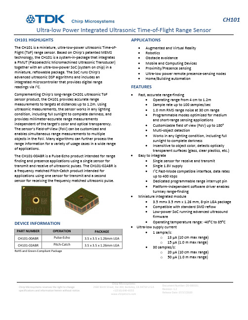
CH101 Ultra-low Power Integrated Ultrasonic Time-of-Flight Range SensorChirp Microsystems reserves the right to change specifications and information herein without notice.Chirp Microsystems2560 Ninth Street, Ste 200, Berkeley, CA 94710 U.S.A+1(510) 640–8155Document Number: DS-000331Revision: 1.2Release Date: 07/17/2020CH101 HIGHLIGHTSThe CH101 is a miniature, ultra-low-power ultrasonic Time-of-Flight (ToF) range sensor. Based on Chirp’s patented MEMS technology, the CH101 is a system-in-package that integrates a PMUT (Piezoelectric Micromachined Ultrasonic Transducer) together with an ultra-low-power SoC (system on chip) in a miniature, reflowable package. The SoC runs Chirp’s advanced ultrasonic DSP algorithms and includes an integrated microcontroller that provides digital range readings via I2C.Complementing Chirp’s long-range CH201 ultrasonic ToF sensor product, the CH101 provides accurate range measurements to targets at distances up to 1.2m. Using ultrasonic measurements, the sensor works in any lighting condition, including full sunlight to complete darkness, and provides millimeter-accurate range measurements independent of the target’s color and optical transparency. The sensor’s Field-of-View (FoV) can be customized and enables simultaneous range measurements to multiple objects in the FoV. Many algorithms can further process the range information for a variety of usage cases in a wide range of applications.The CH101-00ABR is a Pulse-Echo product intended for range finding and presence applications using a single sensor for transmit and receive of ultrasonic pulses. The CH101-02ABR is a frequency matched Pitch-Catch product intended for applications using one sensor for transmit and a second sensor for receiving the frequency matched ultrasonic pulse.DEVICE INFORMATIONPART NUMBER OPERATION PACKAGECH101-00ABR Pulse-Echo 3.5 x 3.5 x 1.26mm LGA CH101-02ABR Pitch-Catch 3.5 x 3.5 x 1.26mm LGA RoHS and Green-Compliant Package APPLICATIONS•Augmented and Virtual Reality•Robotics•Obstacle avoidance•Mobile and Computing Devices•Proximity/Presence sensing•Ultra-low power remote presence-sensing nodes •Home/Building automation FEATURES•Fast, accurate range-finding•Operating range from 4 cm to 1.2m•Sample rate up to 100 samples/sec• 1.0 mm RMS range noise at 30 cm range•Programmable modes optimized for medium and short-range sensing applications•Customizable field of view (FoV) up to 180°•Multi-object detection•Works in any lighting condition, including full sunlight to complete darkness•Insensitive to object color, detects opticallytransparent surfaces (glass, clear plastics, etc.) •Easy to integrate•Single sensor for receive and transmit•Single 1.8V supply•I2C Fast-Mode compatible interface, data rates up to 400 kbps•Dedicated programmable range interrupt pin•Platform-independent software driver enables turnkey range-finding•Miniature integrated module• 3.5 mmx 3.5 mm x 1.26 mm, 8-pin LGA package•Compatible with standard SMD reflow•Low-power SoC running advanced ultrasound firmware•Operating temperature range: -40°C to 85°C •Ultra-low supply current• 1 sample/s:o13 µA (10 cm max range)o15 µA (1.0 m max range)•30 samples/s:o20 µA (10 cm max range)o50 µA (1.0 m max range)Table of ContentsCH101 Highlights (1)Device Information (1)Applications (1)Features (1)Simplified Block Diagram (3)Absolute Maximum Ratings (4)Package Information (5)8-Pin LGA (5)Pin Configuration (5)Pin Descriptions (6)Package Dimensions (6)Electrical Characteristics (7)Electrical Characteristics (Cont’d) (8)Typical Operating Characteristics (9)Detailed Description (10)Theory of Operation (10)Device Configuration (10)Applications (11)Chirp CH101 Driver (11)Object Detection (11)Interfacing to the CH101 Ultrasonic Sensor (11)Device Modes of Operation: (12)Layout Recommendations: (13)PCB Reflow Recommendations: (14)Use of Level Shifters (14)Typical Operating Circuits (15)Ordering Information (16)Part Number Designation (16)Package Marking (17)Tape & Reel Specification (17)Shipping Label (17)Revision History (19)SIMPLIFIED BLOCK DIAGRAMFigure 1. Simplified Block DiagramABSOLUTE MAXIMUM RATINGSPARAMETER MIN. TYP. MAX. UNIT AVDD to VSS -0.3 2.2 V VDD to VSS -0.3 2.2 V SDA, SCL, PROG, RST_N to VSS -0.3 2.2 V Electrostatic Discharge (ESD)Human Body Model (HBM)(1)Charge Device Model (CDM)(2)-2-5002500kVV Latchup -100 100 mA Temperature, Operating -40 85 °C Relative Humidity, Storage 90 %RH Continuous Input Current (Any Pin) -20 20 mA Soldering Temperature (reflow) 260 °CTable 1. Absolute Maximum RatingsNotes:1.HBM Tests conducted in compliance with ANSI/ESDA/JEDEC JS-001-2014 Or JESD22-A114E2.CDM Tests conducted in compliance with JESD22-C101PACKAGE INFORMATION8-PIN LGADESCRIPTION DOCUMENT NUMBER CH101 Mechanical Integration Guide AN-000158CH101 and CH201 Ultrasonic Transceiver Handling andAssembly Guidelines AN-000159Table 2. 8-Pin LGAPIN CONFIGURATIONTop ViewFigure 2. Pin Configuration (Top View)PIN DESCRIPTIONSPIN NAME DESCRIPTION1 INT Interrupt output. Can be switched to input for triggering and calibration functions2 SCL SCL Input. I2C clock input. This pin must be pulled up externally.3 SDA SDA Input/Output. I2C data I/O. This pin must be pulled up externally.4 PROG Program Enable. Cannot be floating.5 VSS Power return.6 VDD Digital Logic Supply. Connect to externally regulated 1.8V supply. Suggest commonconnection to AVDD. If not connected locally to AVDD, b ypass with a 0.1μF capacitor asclose as possible to VDD I/O pad.7 AVDD Analog Power Supply. Connect to externally re gulated supply. Bypass with a 0.1μFcapacitor as close as possible to AVDD I/O pad.8 RESET_N Active-low reset. Cannot be floating.Table 3. Pin DescriptionsPACKAGE DIMENSIONSFigure 3. Package DimensionsELECTRICAL CHARACTERISTICSAVDD = VDD = 1.8VDC, VSS = 0V, T A = +25°C, min/max are from T A = -40°C to +85°C, unless otherwise specified.PARAMETER SYMBOL CONDITIONS MIN TYP MAX UNITSPOWER SUPPLYAnalog Power Supply AVDD 1.62 1.8 1.98 V Digital Power Supply VDD 1.62 1.8 1.98 VULTRASONIC TRANSMIT CHANNELOperating Frequency 175 kHzTXRX OPERATION (GPR FIRMWARE USED UNLESS OTHERWISE SPECIFIED)Maximum Range Max Range Wall Target58 mm Diameter Post1.2(1)0.7mm Minimum Range Min Range Short-Range F/W used 4(2)cm Measuring Rate (Sample/sec) SR 100 S/s Field of View FoV Configurable up to 180º deg Current Consumption (AVDD +VDD) I SSR=1S/s, Range=10 cmSR=1S/s, Range=1.0mSR=30S/s, Range=10 cmSR=30S/s, Range=1.0m13152050μAμAμAμA Range Noise N R Target range = 30 cm 1.0 mm, rms Measurement Time 1m max range 18 ms Programming Time 60 msTable 4. Electrical CharacteristicsNotes:1.Tested with a stationary target.2.For non-stationary objects. While objects closer than 4cm can be detected, the range measurement is not ensured.ELECTRICAL CHARACTERISTICS (CONT’D)AVDD = VDD = 1.8VDC, VSS = 0V, T A = +25°C, unless otherwise specified.PARAMETERSYMBOL CONDITIONS MINTYP MAX UNITS DIGITAL I/O CHARACTERISTICS Output Low Voltage V OL SDA, INT,0.4 V Output High Voltage V OH INT 0.9*V VDD V I 2C Input Voltage Low V IL_I2C SDA, SCL 0.3*V VDDV I 2C Input Voltage High V IH_I2C SDA, SCL 0.7*V VDD V Pin Leakage Current I L SDA,SCL, INT(Inactive), T A =25°C±1μA DIGITAL/I 2C TIMING CHARACTERISTICSSCL Clock Frequencyf SCLI 2C Fast Mode400kHzTable 5. Electrical Characteristics (Cont’d)TYPICAL OPERATING CHARACTERISTICSAVDD = VDD = 1.8VDC, VSS = 0V, T A = +25°C, unless otherwise specified.Typical Beam Pattern – MOD_CH101-03-01 Omnidirectional FoV module(Measured with a 1m2 flat plate target at a 30 cm range)Figure 4. Beam pattern measurements of CH101 moduleDETAILED DESCRIPTIONTHEORY OF OPERATIONThe CH101 is an autonomous, digital output ultrasonic rangefinder. The Simplified Block Diagram, previously shown, details the main components at the package-level. Inside the package are a piezoelectric micro-machined ultrasonic transducer (PMUT) and system-on-chip (SoC). The SoC controls the PMUT to produce pulses of ultrasound that reflect off targets in the sensor’s Field of View (FoV). The reflections are received by the same PMUT after a short time delay, amplified by sensitive electronics, digitized, and further processed to produce the range to the primary target. Many algorithms can further process the range information for a variety of usage cases in a wide range of applications.The time it takes the ultrasound pulse to propagate from the PMUT to the target and back is called the time-of-flight (ToF). The distance to the target is found by multiplying the time-of-flight by the speed of sound and dividing by two (to account for the round-trip). The speed of sound in air is approximately 343 m/s. The speed of sound is not a constant but is generally stable enough to give measurement accuracies within a few percent error.DEVICE CONFIGURATIONA CH101 program file must be loaded into the on-chip memory at initial power-on. The program, or firmware, is loaded through a special I2C interface. Chirp provides a default general-purpose rangefinder (GPR) firmware that is suitable for a wide range of applications. This firmware enables autonomous range finding operation of the CH101. It also supports hardware-triggering of the CH101 for applications requiring multiple transceivers. Program files can also be tailored to the customer’s application. Contact Chirp for more information.CH101 has several features that allow for low power operation. An ultra-low-power, on-chip real-time clock (RTC) sets the sample rate and provides the reference for the time-of-flight measurement. The host processor does not need to provide any stimulus to the CH101 during normal operation, allowing the host processor to be shut down into its lowest power mode until the CH101 generates a wake-up interrupt. There is also a general-purpose input/output (INT) pin that is optimized to be used as a system wake-up source. The interrupt pin can be configured to trigger on motion or proximity.APPLICATIONSCHIRP CH101 DRIVERChirp provides a compiler and microcontroller-independent C driver for the CH101 which greatly simplifies integration. The CH101 driver implements high-level control of one or more CH101s attached to one or more I2C ports on the host processor. The CH101 driver allows the user to program, configure, trigger, and readout data from the CH101 through use of C function calls without direct interaction with the CH101 I2C registers. The CH101 driver only requires the customer to implement an I/O layer which communicates with the host processor’s I2C hardware and GPIO hardware. Chirp highly recommends that all designs use the CH101 driver.OBJECT DETECTIONDetecting the presence of objects or people can be optimized via software, by setting the sensor’s full-scale range (FSR), and via hardware, using an acoustic housing to narrow or widen the sensor’s field-of-view. The former means that the user may set the maximum distance at which the sensor will detect an object. FSR values refer to the one-way distance to a detected object.In practice, the FSR setting controls the amount of time that the sensor spends in the listening (receiving) period during a measurement cycle. Therefore, the FSR setting affects the time required to complete a measurement. Longer full-scale range values will require more time for a measurement to complete.Ultrasonic signal processing using the CH101’s General Purpose Rangefinder (GPR) Firmware will detect echoes that bounce off the first target in the Field-of-View. The size, position, and material composition of the target will affect the maximum range at which the sensor can detect the target. Large targets, such as walls, are much easier to detect than smaller targets. Thus, the associated operating range for smaller targets will be shorter. The range to detect people will be affected by a variety of factors such as a person’s size, clothing, orientation to the sensor and the sensor’s field-of-view. In general, given these factors, people can be detected at a maximum distance of 0.7m from the CH101 sensor.For additional guidance on the detection of people/objects using the NEMA standard, AN-000214 Presence Detection Application Note discusses the analysis of presence detection using the Long-Range CH201 Ultrasonic sensor.INTERFACING TO THE CH101 ULTRASONIC SENSORThe CH101 communicates with a host processor over the 2-wire I2C protocol. The CH101 operates as an I2C slave and responds to commands issued by the I2C master.The CH101 contains two separate I2C interfaces, running on two separate slave addresses. The first is for loading firmware into the on-chip program memory, and the second is for in-application communication with the CH101. The 7-bit programming address is0x45, and the 7-bit application address default is 0x29. The application address can be reprogrammed to any valid 7-bit I2C address. The CH101 uses clock stretching to allow for enough time to respond to the I2C master. The CH101 clock stretches before the acknowledge (ACK) bit on both transmit and receive. For example, when the CH101 transmits, it will hold SCL low after it transmits the 8th bit from the current byte while it loads the next byte into its internal transmit buffer. When the next byte is ready, it releases the SCL line, reads the master’s ACK bit, and proceeds accordingly. When the CH101 is receiving, it holds the SCL line low after it receives the 8th bit in a byte. The CH101 then chooses whether to ACK or NACK depending on the received data and releases the SCL line.The figure below shows an overview of the I2C slave interface. In the diagram, ‘S’ indicates I2C start, ‘R/W’ is the read/write bit, ‘Sr’ is a repeated start, ‘A’ is acknowledge, and ‘P’ is the stop condition. Grey boxes indicate the I2C master actions; white boxes indicate the I2C slave actions.Figure 5. CH101 I2C Slave Interface DiagramDEVICE MODES OF OPERATION:FREE-RUNNING MODEIn the free-running measurement mode, the CH101 runs autonomously at a user specified sample rate. In this mode, the INT pin is configured as an output. The CH101 pulses the INT pin high when a new range sample is available. At this point, the host processor may read the sample data from the CH101 over the I2C interface.HARDWARE-TRIGGERED MODEIn the hardware triggered mode, the INT pin is used bi-directionally. The CH101 remains in an idle condition until triggered by pulsing the INT pin. The measurement will start with deterministic latency relative to the rising edge on INT. This mode is most useful for synchronizing several CH101 transceivers. The host controller can use the individual INT pins of several transceivers to coordinate the exact timing.CH101 BEAM PATTERNSThe acoustic Field of View is easily customizable for the CH101 and is achieved by adding an acoustic housing to the transceiver that is profiled to realize the desired beam pattern. Symmetric, asymmetric, and omnidirectional (180° FoV) beam patterns are realizable. An example beam pattern is shown in the Typical Operating Characteristics section of this document and several acoustic housing designs for various FoV’s are available from Chirp.LAYOUT RECOMMENDATIONS:RECOMMENDED PCB FOOTPRINTDimensions in mmFigure 6. Recommended PCB FootprintPCB REFLOW RECOMMENDATIONS:See App Note AN-000159, CH101 and CH201 Ultrasonic Transceiver Handling and Assembly Guidelines.USE OF LEVEL SHIFTERSWhile the use of autosense level shifters for all the digital I/O signal signals is acceptable, special handling of the INT line while using a level shifter is required to ensure proper resetting of this line. As the circuit stage is neither a push-pull nor open-drain configuration (see representative circuit below), it is recommended that level shifter with a manual direction control line be used. The TI SN74LVC2T45 Bus Transceiver is a recommended device for level shifting of the INT signal line.Figure 7. INT Line I/O Circuit StageTYPICAL OPERATING CIRCUITSFigure 8. Single Transceiver OperationFigure 9. Multi- Transceiver OperationORDERING INFORMATIONPART NUMBER DESIGNATIONFigure 10. Part Number DesignationThis datasheet specifies the following part numbersPART NUMBER OPERATION PACKAGE BODY QUANTITY PACKAGING CH101-00ABR Pulse-Echo 3.5 mm x 3.5 mm x 1.26 mmLGA-8L 1,000 7” Tape and ReelCH101-02ABR Pitch-Catch 3.5 mm x 3.5 mm x 1.26 mmLGA-8L 1,000 7” Tape and ReelTable 6. Part Number DesignationCH101-xxABxProduct FamilyProduct Variant Shipping CarrierR = Tape & Reel 00AB = Pulse-Echo Product Variant02AB = Pitch-Catch Product VariantCH101 = Ultrasonic ToF SensorPACKAGE MARKINGFigure 11. Package MarkingTAPE & REEL SPECIFICATIONFigure 12. Tape & Reel SpecificationSHIPPING LABELA Shipping Label will be attached to the reel, bag and box. The information provided on the label is as follows:•Device: This is the full part number•Lot Number: Chirp manufacturing lot number•Date Code: Date the lot was sealed in the moisture proof bag•Quantity: Number of components on the reel•2D Barcode: Contains Lot No., quantity and reel/bag/box numberDimensions in mmDEVICE: CH101-XXXXX-XLOT NO: XXXXXXXXDATE CODE: XXXXQTY: XXXXFigure 13. Shipping LabelREVISION HISTORY09/30/19 1.0 Initial Release10/22/19 1.1 Changed CH-101 to CH101. Updated figure 7 to current markings.07/17/20 1.2 Format Update. Incorporated “Maximum Ratings Table” and “Use of LevelShifters” section.This information furnished by Chirp Microsystems, Inc. (“Chirp Microsystems”) is believed to be accurate and reliable. However, no responsibility is assumed by Chirp Microsystems for its use, or for any infringements of patents or other rights of third parties that may result from its use. Specifications are subject to change without notice. Chirp Microsystems reserves the right to make changes to this product, including its circuits and software, in order to improve its design and/or performance, without prior notice. Chirp Microsystems makes no warranties, neither expressed nor implied, regarding the information and specifications contained in this document. Chirp Microsystems assumes no responsibility for any claims or damages arising from information contained in this document, or from the use of products and services detailed therein. This includes, but is not limited to, claims or damages based on the infringement of patents, copyrights, mask work and/or other intellectual property rights.Certain intellectual property owned by Chirp Microsystems and described in this document is patent protected. No license is granted by implication or otherwise under any patent or patent rights of Chirp Microsystems. This publication supersedes and replaces all information previously supplied. Trademarks that are registered trademarks are the property of their respective companies. Chirp Microsystems sensors should not be used or sold in the development, storage, production or utilization of any conventional or mass-destructive weapons or for any other weapons or life threatening applications, as well as in any other life critical applications such as medical equipment, transportation, aerospace and nuclear instruments, undersea equipment, power plant equipment, disaster prevention and crime prevention equipment.©2020 Chirp Microsystems. All rights reserved. Chirp Microsystems and the Chirp Microsystems logo are trademarks of Chirp Microsystems, Inc. The TDK logo is a trademark of TDK Corporation. Other company and product names may be trademarks of the respective companies with which they are associated.©2020 Chirp Microsystems. All rights reserved.。

专利名称:ADAPTIVE WRITE ACKNOWLEDGMENT FORSTORAGE DEVICES发明人:Bishwajit DUTTA,Sanjeev N. TRIKA,Anand S.RAMALINGAM,Pallav H. GALA申请号:US16855139申请日:20200422公开号:US20200249980A1公开日:20200806专利内容由知识产权出版社提供专利附图:摘要:Examples include techniques for managing high priority (HP) and low priority (LP) write transaction requests by a storage device. An embodiment includes receiving, ata storage controller for a storage device, a write transaction request from a requestor to write data to one or more memory devices in the storage device. When the write transaction request is for a high priority (HP) write, coalescing the write data into a transaction buffer in a memory of the storage device, sending an acknowledgment for the write transaction request to the requestor, and writing the write data into the one or more memory devices. When the write transaction request is for a low priority (LP) write, writing the write data into the one or more memory devices, and then sending an acknowledgment for the write transaction request to the requestor.申请人:Intel Corporation地址:Santa Clara CA US国籍:US更多信息请下载全文后查看。

堆叠自动编码器的特征选择方法自动编码器是一种无监督学习算法,可以用于特征提取和数据降维。
堆叠自动编码器是由多个自动编码器组成的深度神经网络,通过层层训练来学习数据的高级抽象特征。
在实际应用中,特征选择是非常重要的,可以帮助我们减少数据维度,提高模型效率和预测准确率。
本文将探讨堆叠自动编码器的特征选择方法。
一、特征选择的意义特征选择是指从原始数据中选择出最具代表性的特征,排除冗余和噪声,以提高模型的泛化能力和预测性能。
在实际应用中,原始数据往往包含大量特征,而其中只有一部分特征对模型的训练和预测起到关键作用。
因此,通过特征选择可以减少数据维度,提高模型训练效率,降低过拟合的风险。
二、堆叠自动编码器的特征提取堆叠自动编码器是一种深度神经网络,可以用于学习数据的高级抽象特征。
在训练过程中,每一层自动编码器都能够学习数据的不同层次的特征表示,从而实现数据的逐层抽象和提取。
通过堆叠多个自动编码器,可以逐渐提取出数据的深层次特征,这些特征对于区分不同类别的数据具有很强的区分能力。
三、基于重构误差的特征选择方法在堆叠自动编码器中,每个自动编码器的训练都是通过最小化重构误差来实现的。
重构误差指的是输入数据与自动编码器的重构输出之间的差异,通过最小化重构误差,可以有效地学习数据的抽象特征表示。
因此,可以基于重构误差来进行特征选择,具体方法是通过分析每个特征对于重构误差的贡献程度,选择对重构误差影响较大的特征作为最终的特征集合。
四、基于梯度下降的特征选择方法除了基于重构误差的方法,还可以利用梯度下降的方法来进行特征选择。
在堆叠自动编码器的训练过程中,可以通过计算每个特征对于损失函数的梯度,来评估每个特征对于模型训练的重要性。
通过梯度下降的方法,可以筛选出对于损失函数梯度影响较大的特征,从而实现特征选择的目的。
五、正则化方法的特征选择在堆叠自动编码器的训练过程中,可以通过正则化方法来进行特征选择。
正则化方法可以通过添加惩罚项来约束模型的复杂度,从而实现对特征的选择和筛选。

halcon畸变校正adaptive算法原理-回复Halcon (海康) 是一种用于机器视觉应用的强大的软件库。
它提供了广泛的图像处理和分析功能,包括畸变校正(Distortion Correction) 算法。
畸变校正在机器视觉中非常重要,因为它可以去除图像中由镜头畸变引起的形变,从而提高图像的准确性和可靠性。
在Halcon中,adaptive算法是一种常用的畸变校正方法。
本文将逐步介绍adaptive算法的原理及其应用。
第一节:畸变校正基础畸变校正是通过转换像素坐标来纠正图像中的形状失真。
镜头畸变主要包括径向畸变和切向畸变。
径向畸变是由于镜头形状引起的,会使得图像中的直线弯曲或弯曲。
切向畸变是由于镜头放置角度引起的,会导致图像中的直线扭曲或倾斜。
畸变校正的目标是将图像重新映射到一个平面上,使得图像中的直线变为直的。
畸变校正方法通常包括建立畸变模型和对图像进行数学变换两个步骤。
第二节:adaptive算法原理adaptive算法是一种自适应的畸变校正方法,它可以根据已知的畸变模型参数自动调整校正结果,以减小残余畸变。
adaptive算法的原理基于对畸变模型的灵活性进行优化。
adaptive算法包括以下主要步骤:1. 提供已知的畸变模型参数,包括径向畸变系数和切向畸变系数。
这些参数可以通过镜头制造商提供的校准数据或通过标定板的图像处理得到。
2. 将待校正的图像分割成小的校正区域。
这可以通过图像中的特定特征或用户定义的区域来完成。
3. 对于每个校正区域,计算出原始图像中的坐标和校正后图像中的坐标之间的映射关系。
这通常使用畸变模型参数来进行计算。
具体算法包括对原始图像的每个像素进行反向畸变计算,并查找最近邻像素来获得校正后图像中的坐标。
4. 根据映射关系对图像进行数学变换。
这通常包括对校正后图像进行插值来生成新的校正图像。
插值方法可以根据应用需求进行选择,常见的插值方法有双线性插值和双三次插值等。
5. 对校正图像进行残余畸变分析。

S p e C S H e e tkey feAtureSHigh accuracy, wide dynamic range and high power measurement capability (up to 26 dBm)Memory capacity of 1000 data items; enables data transfer to a PC via USB connectionUser-configurable pass/fail thresholds with LED indicator Over 40 calibrated wavelengths, and hold Min/Max power functionRechargeable batteriesError-free, time-saving test features: automatic wavelength switching, no offset nulling Low cost of ownership: three-year warranty and recommended calibration intervalfpm-600POWER METER2014GLOBALPORTABLE FIBER OPTIC T EST EQUIPMENTMARKET LEADERSHIPAWARDSuited for All Network typeSThe FPM-600 is a very powerful tool for the most demanding applications such as high-speed DWDM or CWDM network qualification.With more than 40 calibrated wavelengths, including all CWDM wavelengths, it allows for user-defined measurement wavelengths, using the interpolation method between calibrated points. Use its Hold Min/Max Power function to measure system power burst or fluctuations.error-free, time SA viNg teSt f eAtureSWhen used in combination with a FLS-600 Light Source in Auto-Switching mode, the power meter automatically recognizes the wavelength in use and switches to the proper calibration parameter. At the press of a button, you can store results for all wavelengths at once.fttx reAdyE XFO’s FPM-600 allows for the testing of passive optical networks (PONs) at 1310 nm, 1490 nm and 1550 nm, the three wavelengths recommended by the ITU-T (G.983.3) for PONs.at once.rugged A N d verSAtileLike all EXFO portable instruments, the FPM-600 is built for top ruggedness and versatility, perfect for the harshest test conditions. It features a keypad/LCD backlight, for easy operation in darker environments. What’s more, it is powered by a rechargeable battery.reportiNg SoftwAreThis new software tool enables you to produce professional-looking reports with comprehensive documentation. It also offers these functionalities:› T wo test files can be merged into one test report (see note no. 3)› P ass/fail thresholds that are active during download are automatically activated and displayed in the Report Viewer › O ne-touch storage of results for all wavelengths at once (see note no. 1)› U nit B configuration information can be input and documented (see note no. 2)› D ata transfer can be launched from the Report Viewer window (see note no. 3)› Apass/fail threshold can be set for an individual fiber or wavelength (see note no. 4)Optical Report Viewer: main w indow23Launchdata transfer and converter/mergerConfigure unit B information1Store test results for all wavelengths at onceOptical Report Viewer: main w indowSelect all or no results in a specific sectionApply a specific threshold to each fiber and/or wavelength and get a complete pass/fail status (not available with FasTesT results)4Notesa.Guaranteed unless otherwise specified. All specifications valid at 1550 nm and 23 °C ± 1 °C, with an F C connector.b.In C W mode; sensitivity defined as 6 x rms noise level.c.For calibrated wavelengths. Valid up to 20 dBm for FPM-602X.d.For power > –40 dBm for FPM-602, and > –25 dBm for FPM-602X.e.At 850 nm, 1300 nm, 1310 nm, 1490 nm, 1550 nm and 1650 nm; for power > –50 dBm for FPM-602 and > –40 dBm (typical) for FPM-602X.f.For a variation of ≤ 0.06 dB at power levels ≥ –40 dBm for FPM-602 and ≥ –25 dBm for FPM-602X.S P E C I F I C A T I O N S aModel FPM-602FPM-602X DetectorGe GeX Power range (dBm) b 10 to –7026 to –55Wavelength range (nm)800 to 1650800 to 1650Calibrated wavelengths (nm)800, 820, 830, 840, 850, 860, 870, 880, 910, 980, 1270,Same calibrated wavelengths as the FPM-602, plus 10601280, 1290, 1300, 1310, 1320, 1330, 1340, 1350, 1370,1390, 1410, 1430, 1450, 1460, 1470, 1480, 1490, 1500,1510, 1520, 1530, 1540, 1550, 1560, 1570, 1580, 1590,1600, 1610, 1620, 1630, 1640, 1650Power uncertainty c ±5 % ± 0.1 nW±5 % ± 3 nWResolution (dB)±0.01 (10 dBm to –60 dBm)±0.01 (26 dBm to –45 dBm)Automatic offset nulling d Yes Yes Display units dB, dBm, WdB, dBm, WTone detection 270 Hz, 1 kHz and 2 kHz 270 Hz, 1 kHz and 2 kHz Auto-switching eYes Yes Warm-up period (min) f 0Data storage (items)More than 1000More than 1000Battery life (hours) (typical)7272Warranty and recommended recalibration interval (years)33Optical Report Viewer: main w indowO R D E R I N G I N F O R M A T I O NG E N E R A L S P E C I F I C A T I O N SSize (H x W x D)190 mm x 100 mm x 55 mm (7 ½ in x 4 in x 2 ⅛ in)Weight (with battery)0.48 kg (1.1 lb)Temperature operatingstorage–10 °C to 50 °C (14 °F to 122 °F)–40 °C to 70 °C (–40 °F to 158 °F)Relative humidity0 % to 95 % noncondensingS T A N D A R D A C C E S S O R I E SUser guide, Certificate of Calibration, instrument stickers in six languages, A C adapter/charger, lithium ion battery, shoulder strap, carrying case, U S B cable.L A S E R S A F E T YIEC 60825-1:200721 CFR 1040.10LASER RADIATION A V O I D DIRECT EYE EXPOSURE CLASS 3R LASER P R O D U C T: 650 ±10 n mP o u t maximum < 5m W (into free space)。

Accelerate Software-Defined Networking Provide Security from Edge to CoreNVIDIA ASAP2 technology accelerates software-defined networking, delivering line-rate performance with no CPU penalty.Hardware engines in ConnectX-7 offload and accelerate security, with in-line encryption/decryption of TLS, IPsec, and MACsec.Enhance Storage Performance Enable Precision TimingConnectX-7 enables high-performance storage and data access with RoCE and GPUDirect Storage and accelerates NVMe-oF over both RoCE and TCP.ConnectX-7 provides extremely accurate time synchronization for data-center applications and timing-sensitive infrastructures.NVIDIA CONNECTX-7 400G ETHERNETSMART ACCELERATION FOR CLOUD, DATA-CENTER AND EDGEACCELERATED NETWORKING AND SECURITY FOR THE MOST ADVANCED CLOUD AND AI WORKLOADSThe NVIDIA® ConnectX®-7 SmartNIC is optimized to deliver accelerated networking for modern cloud, artificial intelligence, and traditional enterprise workloads. ConnectX-7 provides a broad set of software-defined, hardware accelerated networking, storage, and security capabilities which enable organizations to modernize and secure their IT infrastructures.Extending the tradition of NVIDIA’s industry leading innovation for networking, ConnectX-7, is available in 1, 2, or 4-port configurations and delivers up to 400Gb/s of bandwidth. With features such as NVIDIA ASAP2 - Accelerated Switching and Packet Processing®, advanced RoCE, NVIDIA GPUDirect® Storage, and in-line hardware acceleration for TLS/IPsec/MACsec encryption/decryption, ConnectX-7 empowers agile and high-performance solutions from edge to core data centers to clouds, all while enhancing network security and reducing the total cost of ownership.Available in PCIe card and OCP3.0 form factors, ConnectX-7 empowers solutions for cloud, hyperscale, and enterprise networking.PRODUCT SPECIFICATIONSMaximum TotalBandwidth400GbESupported EthernetSpeeds10/25/40/50/100/200/400GbE Number ofNetwork Ports1/2/4Network InterfaceTechnologiesNRZ (10/25G) / PAM4(50/100G)Host Interface PCIe Gen5.0 x16/ x32Cards Form Factors PCIe FHHL/ HHHL,OCP3.0 SFF Network Interfaces SFP56, QSFP56,QSFP56-DD,QSFP112, SFP112NVIDIA CONNECTX-7 | DATASHEET | APR21Network Interface>Up to 4 network ports supporting NRZ, PAM4 (50G and 100G), in various ports configurations:>1 x 10/25/40/50/100/200/400GbE>2 x 10/25/40/50/100/200/400GbE>4 x 10/25/40/50/100/200GbE>Up to 400Gb/s total bandwidthHost Interface>32 lanes of PCIe Gen 5.0, compatible with PCIe Gen 2/3/4>Integrated PCI switch>NVIDIA Multi-Host™ (up to 8 hosts)and NVIDIA Socket Direct™>MSI/MSI-X mechanisms>Advanced PCIe capabilities Networking>RoCE, Zero Touch RoCE>ASAP² - Accelerated Switch and Packet>Processing® for SDN and VNF acceleration >Single Root I/O Virtualization (SR-IOV)>VirtIO acceleration>Overlay network acceleration:VXLAN, GENEVE, NVGRE>Programmable flexible parser:user-defined classification>Connection tracking (L4 firewall)>Flow mirroring, sampling and statistics>Header rewrite>Hierarchical QoS>Stateless TCP offloadsVNF Acceleration>Hardware offload programmable pipeline:>Packet classification on network layersL2 to L4 and tunneled traffic such as GTPand VXLAN>Packet dispatching to multiple cores>Multi-threaded API for concurrent updateof offloaded rules>ASAP2 accelerations/actions: counters,QoS, NAT, aging, mirroring, sampling,flow tag>Hairpin flow for full hardware offload>Highly-scalable number of classificationsand actions>Application access to hardware statistics>Application access to crypto offloadsCyber Security>IInline hardware IPsec encryptionand decryption>AES-GCM 128/256-bit key>IPsec over RoCE>Inline hardware TLS encryptionand decryption>AES-GCM 128/256-bit key>Inline hardware MACsec encryption anddecryption>AES-GCM 128/256-bit key>AES-GCM-XPN 128/256-bit key>Data-at-rest AES-XTS encryptionand decryption>AES-XTS 256/512-bit key>Platform security>Secure boot with hardware root-of-trust>Secure firmware update>On-board flash encryptionAdvanced Timing andSynchronization>Advanced PTP>IEEE 1588v2 (any profile)>Meets G.8273.2 Class C standard>PTP hardware clock (PHC) (UTC format)>12 nanosecond accuracy>Line-rate hardware timestamp(UTC format)>SyncE>Meets G.8262.1 (eEEC)>Configurable PPS In and configurablePPS Out>Time-triggered scheduling>PTP-based packet pacing>Time-based SDN acceleration (ASAP2)Storage Accelerations>NVMe™ over Fabrics (NVMe-oF) storagetarget offloads>NVMe-oF™ over TCP/RoCE acceleration>Storage protocols: iSER, NFSoRDMA, SMBDirect, NVMe-oF™, and moreHPC / AI>All-to-All engine>NVIDIA GPUDirect>NVIDIA GPUDirect StorageManagement and Control>SMBus 2.0>Network Controller SidebandInterface (NC-SI)>NC-SI, MCTP over SMBus and MCTPover PCIe - Baseboard ManagementController interface>PLDM for Monitor and Control DSP0248>PLDM for Firmware Update DSP026>I2C interface for device controland configuration>General Purpose I/O pins>SPI interface to flash>JTAG IEEE 1149.1 and>IEEE 1149.6Remote Boot>Remote boot over Ethernet>Remote boot over iSCSI>UEFI support for x86 and Arm servers>PXE bootForm Factors and Options>PCIe HHHL/FHHL>OCP 3.0 SFFFEATURESTo learn more about the NVIDIA ConnectX SmartNICs visit /en-us/networking/ethernet-adapters/© 2021 NVIDIA Corporation. All rights reserved. NVIDIA, the NVIDIA logo, ConnectX, ConnectX-7, GPUDirect, Multi-Host, Socket Direct, and ASAP2 - Accelerated Switch and Packet Processing are trademarks and/or registered trademarks of NVIDIA Corporation in the U.S. and other countries. Other company and product names may be trademarks of the respective companies with which they are associated. MAY21.。

adaptivethreshold 偏移量-回复什么是adaptivethreshold 偏移量?Adaptivethreshold 偏移量(Adaptive Threshold Offset)是一种图像处理中常用的技术,用于将图像分割为二值图像。
图像分割是图像处理的基础步骤之一,它将图像中的目标和背景分离出来,使得图像更容易理解和处理。
在进行图像分割时,常常需要选择一个合适的阈值来确定目标和背景,而adaptivethreshold 偏移量就是用来计算这个阈值的。
为了更好地理解adaptivethreshold 偏移量的作用,首先需要了解adaptivethreshold 分割算法的工作原理。
这一算法是基于自适应阈值的分割方法,它可以根据图像中的像素灰度值的局部特性自动选择阈值,从而实现更好的分割效果。
adaptivethreshold 分割算法根据像素周围的邻域信息来确定每个像素的阈值,这使得它能够在受到光照和噪声等因素影响时仍能有效地进行图像分割。
具体而言,adaptivethreshold 偏移量是用来调整adaptivethreshold 算法中的阈值的。
adaptivethreshold 算法根据图像局部邻域的平均灰度值来计算阈值,而adaptivethreshold 偏移量可以对这个计算结果进行修正。
当我们在使用adaptivethreshold 算法进行图像分割时,可能会遇到一些特殊情况,例如图像中存在很强的光照差异或者噪声干扰较多。
这些情况下,adaptivethreshold 的计算结果可能会偏离我们期望的分割效果,因此我们需要根据实际情况调整阈值。
adaptivethreshold 偏移量可以通过增加或减少adaptivethreshold 算法中的阈值来实现。
当图像中存在较强光照差异时,我们可以增加偏移量来使得阈值增加,从而更好地适应光照变化。
而当图像中存在噪声干扰时,我们可以减少偏移量来使得阈值减小,从而更好地保留目标的细节信息。

Adaptive Scan with On-Chip ClockingApplication NoteY-2006.06OverviewThis application note describes a workaround for the automated flow for Adaptive Scan (DFT MAX) with On-Chip Clocking (OCC) Support. The flow which is described here is currently the only way to get two independent test mode controls, one for compression vs. normal-scan modes and the other for PLL test mode. This flow also avoids top-level logic, which the automated flow adds.This application note covers the insertion of Adaptive Scan and OCC, the generation and manual modifications of test-protocols for various test-modes and the automatic pattern generation (ATPG) on a hierarchical example design. BackgroundThe example design in this application note has two top level blocks, one core and a clock-generator block. Adaptive Scan should be inserted to the core block and the DesignWare IP clock controller and clock chain should be synthesized into the clock-generator block. There should be no glue-logic on the top level.To simplify the process, we will do the Adaptive Scan- and OCC-insertion in a hierarchical flow in separate steps. Adaptive Scan will be inserted on the core level and the OCC-controller and clock-chain will be inserted in the clock-generator block. The top-level connections will have to be made by the user, see Figure 1: Design Block Diagram.In this example we want to have three test modes:1. Pure scan without OCC support(using the test clock for scan shifting and capture)2. Adaptive Scan compression without OCC support(using the test clock for scan shifting and capture)3. Adaptive Scan compression with OCC support(using the test clock for shifting and the PLL clocks for launch & capture)Figure 1: Design Block DiagramTest Ports ConsiderationsBefore inserting Adaptive Scan and OCC we should consider the required test ports, so that we can already create them in our RTL code together with the top-level connections to the two sub-blocks.For Adaptive Scan we need Scan-In and Scan-Out ports to feed the scan-compression logic and the reconfigured scan-chains. We also need a test-mode signal to switch between the scan-compression mode and the reconfigured scan mode (pure scan). In this example we are using 5 Scan-In/Scan-Out pairs (test_si[0..4], test_so[0..4]), a Scan-Enable (test_se) and the test-mode port (test_mode_compr).For the OCC controller we need a separate test-mode signal (test_mode_occ) to activate the OCC controller in test mode. Beside the reference-clock (ref_clk), which feeds the PLLs, we need one test-clock (ate_clk) for scan-shifting. A PLL-bypass signal is used to bypass the PLLs and feed through the test-clock to the scan-cells (test_pll_bypass). The OCC controller requires the Scan-Enable (test_se) and a PLL-reset to reset the controller. In this example the PLL-reset isshared with the active high chip reset (rst).Because the Clock-Chain cannot be included to the Adaptive Scan chains, we need separate Scan-In and Scan-Out ports. In this design we only want a single Clock-Chain (test_clk_chain_in, test_clk_chain_out).Table 1: Test Access Portstest_si[0..4] Scan Data Intest_so[0..4] Scan Data Outtest_clk_chain_in Clock-Chain Intest_clk_chain_out Clock-Chain Outtest_se Scan-Enabletest_mode_compr Test-Mode Scancompressiontest_mode_occ Test-Mode On-Chip-Clockingtest_pll_bypass PLL-Bypassref_clk Reference Clockate_clk Test Clockrst ResetOCC Controller and Clock-Chain InsertionThis section describes the insertion of the OCC controller and the Clock-Chain. We are starting with a test-ready netlist, all flip-flops in the design have been replaced by scan-flops. The clock-generator block in this example contains a PLL-module, which generates three PLL clocks (clka, clkb and clkc). The PLL itself is triggered by one reference clock (ref_clk). The designer has already created the ports for the OCC controller and Clock-Chain (ate_clk, test_mode_occ, pll_reset, test_pll_bypass, test-se, test_clk_chain_in, test_clk_chain_out).Figure 2 : clock-generator block before OCC controller insertionIn this design we want to insert a single OCC controller and one Clock-Chain for all three PLL-clocks with two capture cycles per clock. We are following the instructions from the DFT Compiler User Guide Vol.1: Scan (XG Mode), section On-Chip Clocking Support:current_design clock_genset_dft_configuration -clock_controller enableset_dft_signal -view existing -type Oscillator -hookup_pin pll_module/clkaset_dft_signal -view existing -type Oscillator -hookup_pin pll_module/clkbset_dft_signal -view existing -type Oscillator -hookup_pin pll_module/clkcset_dft_signal -view existing -type Oscillator -port ref_clkset_dft_signal -view existing -type Oscillator -port ate_clkset_dft_signal -view existing -type ScanClock -port ate_clk -timing { 45 55 } set_dft_signal -view spec -type pll_bypass -port test_pll_bypassset_dft_signal -view spec -type pll_reset -port pll_resetset_dft_clock_controller -cell_name pll_controller1 -design snps_clk_mux \-pllclocks { pll_module/clka pll_module/clkb pll_module/clkc } \-ateclocks { ate_clk } -cycles_per_clock 2 -chain_count 1set_dft_signal -view spec -type TestMode -port test_mode_occset_dft_signal -view spec -type ScanEnable -port test_seset_dft_signal -view spec -type ScanDataIn -port test_clk_chain_inset_dft_signal -view spec -type ScanDataOut -port test_clk_chain_outcreate_test_protocoldft_drcpreview_dftinsert_dftchange_names -rule verilogwrite -f verilog -h -o ./netlist/occ.vwrite_test_protocol -test_mode Internal_scan -o ./atpg/clock_gen_occ.spfwrite_test_protocol -test_mode Internal_scan -o ./atpg/clock_gen_pll_bypass.spf -pll_bypassScan Compression InsertionThis section describes the scan compression insertion on the core-level. The core-level contains the core logic and the designer has already created the test access ports (test_se, test_si[0..4], test_so[0..4], test_mode_compr). We are following the standard Adaptive Scan flow, which is described in the Design Compiler User Guide Vol.2: Adaptive Scan (XG Mode). We want 5 Scan-In/Scan-Out pairs with the default compression factor of 10x.Figure 3: core block before insertioncurrent_design coreset scan_chains 5set_dft_configuration -scan_compression enableset_scan_configuration -chain_count $scan_chainsset_dft_signal -view existing -type ScanClock -port clk1 -timing { 45 55 }set_dft_signal -view existing -type ScanClock -port clk2 -timing { 45 55 }set_dft_signal -view existing -type ScanClock -port clk3 -timing { 45 55 }set_dft_signal -view existing -type Reset -port rst -active 1for {set i 0} {$i<$scan_chains} {incr i} {set_dft_signal -view spec -type ScanDataIn -port test_si[$i]set_dft_signal -view spec -type ScanDataout -port test_so[$i]}set_dft_signal -view spec -type ScanEnable -port test_seset_dft_signal -view spec -type TestMode -port test_mode_comprcreate_test_protocoldft_drcpreview_dftinsert_dftchange_names -rule verilogwrite -f ddc -h -o ./netlist/core_dftmax.ddcwrite_test_model -o ./netlist/core_dftmax.ctldbwrite_test_protocol -o ./atpg/core_scan.spf \-test_mode Internal_scanwrite_test_protocol -o ./atpg/core_scancompression.spf \-test_mode ScanCompression_modeTest DRC on Top-LevelThis section describes the top level test DRC for the reconfigured scan mode and PLL bypassed. After the Adaptive Scan- and OCC controller insertion we will now go to the top level and use the ‘existing scan’ flow to perform a test DRC. For this purpose we will constrain the design to the reconfigured scan mode (scan compression disabled) and bypass the PLL (ate_clk used for scan-shift and capture).To bring the design into the reconfigured scan mode we have to set the scan compression test mode signal to ‘0’ (test_mode_compr = ‘0’). To bypass the PLL we have to set the OCC test mode signal (test_mode_occ = ‘1’) and the PLL bypass signal (test_pll_bypass = ‘1’).If the DRC passes successfully, we can write out our first top level test protocol for pure scan without OCC support.set scan_chains 5current_design toplinkset_scan_state scan_existingset_dft_signal -view existing -type ScanClock -port ate_clk -timing { 45 55 } set_dft_signal -view existing -type Constant -port rst -active 0 set_dft_signal -view existing -type Constant -port test_mode_occ -active 1 set_dft_signal -view existing -type Constant -port test_pll_bypass -active 1 set_dft_signal -view existing -type Constant -port test_mode_compr -active 0 set_dft_signal -view existing -type ScanEnable -port test_sefor {set i 0} {$i<$scan_chains} {incr i} {set_scan_path chain$i -view existing -scan_data_in test_si[$i] \-scan_data_out test_so[$i] -infer_dft_signals}set_scan_path clock_chain -view existing -scan_data_in test_clk_chain_in \-scan_data_out test_clk_chain_out -infer_dft_signalscreate_test_protocoldft_drcchange_names -rule verilogwrite -f verilog -h -o ./netlist/final_netlist.vwrite -f ddc -h -o ./netlist/final_netlist.ddcwrite_test_protocol -o ./atpg/top_pure_scan_without_occ.spfGenerating the Test Protocols for ATPGThis section describes the manual steps which are necessary to create the test protocols for the scan compression ATPG with and without the OCC support. The insertion of Adaptive Scan and the OCC controller and Clock-Chain above was quite simple. It was also not a big effort to generate the top level test protocol for pure scan without OCC, see last section. Unfortunately the creation of the top level test protocols for the scan compression with OCC is a little bit complex because we have to merge the block level protocols for OCC and Adaptive Scan and map them to the top-level. This process is not that automated yet and requires some hand editing.Test Protocol for Adaptive Scan without OCCWe have already written out a test protocol for Adaptive Scan on the core level. Or task now is to map the scan structure information from this file to the top levelprotocol. In this design we have used the same test port names at the core block and at the top level so no renaming is necessary. Beside the Adaptive Scan structures, the new protocol should also contain the Clock-Chain. In this mode the Clock-Chain behaves like a normal scan chain. To create the protocol we follow these steps:1. Copy ./atpg/top_pure_scan_without_occ.spfto ./atpg/top_scancompression_without_occ.spf2. Delete the ScanStructures block3. Replace it with copies of these blocks (complete)from ./atpg/core_scancompression.spfScanStructures {[...]}UserKeywords CompressorStructures;CompressorStructures {[...]}4. Add the Clock-Chain to the ScanStructures block:[...]ScanStructures {ScanChain "clock_chain" {ScanIn "test_clk_chain_in";ScanOut "test_clk_chain_out";}[...]5. Change every instance of "test_mode_compr"=0; to"test_mode_compr"=1;6. Add the line “ActiveScanChains core_group;” to the top of the"load_unload" Procedure:[...]Procedures {"load_unload" {ActiveScanChains core_group;W "_default_WFT_";[...]Test Protocol for Adaptive Scan with OCCThis is the most complex task in our flow. The first step is to create a top level test protocol for OCC and pure scan. We are using the TetraMAX Quick-STIL feature to generate a template, which has to be modified by hand. The following TetraMAX commands are used to generate the template:read netlist ./library/lib.vread netlist ./library/pll.vread netlist ./netlist/final_netlist.vrun build topset drc -num_pll_cycles 2set atpg -min_refclock_cycles 5add clock 0 ate_clk -shift -refclock -timing 100 45 55 20add clock 0 ref_clk -refclock -shift -timing 100 45 55 20add clock 0 U_clock_gen/pll_module/clka -pllclockadd clock 0 "U_clock_gen/pll_controller1/U2/Z" -intclock \-pll_source U_clock_gen/pll_module/clka \-cycle 0 "U_clock_gen/snps_clk_chain_0/U_ctr_i_0/FF_4/Q" 1 \-cycle 1 "U_clock_gen/snps_clk_chain_0/U_ctr_i_0/FF_5/Q" 1add clock 0 U_clock_gen/pll_module/clkb -pllclockadd clock 0 "U_clock_gen/pll_controller1/U4/Z" -intclock \-pll_source U_clock_gen/pll_module/clkb \-cycle 0 "U_clock_gen/snps_clk_chain_0/U_ctr_i_0/FF_2/Q" 1 \-cycle 1 "U_clock_gen/snps_clk_chain_0/U_ctr_i_0/FF_3/Q" 1add clock 0 U_clock_gen/pll_module/clkc -pllclockadd clock 0 "U_clock_gen/pll_controller1/U6/Z" -intclock \-pll_source U_clock_gen/pll_module/clkc \-cycle 0 "U_clock_gen/snps_clk_chain_0/U_ctr_i_0/FF_0/Q" 1 \-cycle 1 "U_clock_gen/snps_clk_chain_0/U_ctr_i_0/FF_1/Q" 1add scan enable 1 test_seadd pi constraints 1 test_mode_occadd pi constraints 0 test_pll_bypassadd pi constraints 0 rstadd pi constraints 0 test_seadd pi constraints 0 test_mode_compradd scan chain scan_chain_0 test_si[0] test_so[0]add scan chain scan_chain_1 test_si[1] test_so[1]add scan chain scan_chain_2 test_si[2] test_so[2]add scan chain scan_chain_3 test_si[3] test_so[3]add scan chain scan_chain_4 test_si[4] test_so[4]add scan chain clk_chain test_clk_chain_in test_clk_chain_outrun drcwrite drc ./atpg/template_top_pure_scan_with_occ.spf -replacequitThe information about the -intclock, -pll-source and –cycle for the clock controller is taken from the “PLLStructures” in the core level OCC protocol (./atpg/clock_gen_occ.spf). Please note that we have to apply the complete top level paths to the the -intclock, -pll-source and –cycle, see Figure 4: converting protocol to TetraMAX commands. The ‘run drc‘ will fail because of a missing preamble clock pulse in the load_unload procedure and a missing reset execution in the test_setup. Despite the failing ‘run drc‘ we save the protocol as a template (./atpg/template_top_pure_scan_with_occ.spf).Figure 4: converting protocol to TetraMAX commandsThe second step is to edit the template and add the missing preamble clock pulse in the load_unload procedure and execute the reset in the test_setup procedure:[...]Procedures {"load_unload" {W "_default_WFT_";C { "test_si[1]"=0; "test_so[4]"=X; "test_si[0]"=0; "test_so[3]"=X;"test_clk_chain_out"=X;"test_so[2]"=X; "test_si[4]"=0; "test_so[1]"=X; "test_si[3]"=0;"test_so[0]"=X; "test_si[2]"=0; "test_clk_chain_in"=0; "ate_clk"=0;"ref_clk"=0; "test_se"=1; }V { "ate_clk"=P; "ref_clk"=P; }Shift { W "_default_WFT_";V { "_si"=######; "_so"=######; "ate_clk"=P; "ref_clk"=P; }}}[...]MacroDefs {"test_setup" {W "_default_WFT_";V { "test_mode_occ"=1; "test_mode_compr"=0; "test_se"=0;"test_pll_bypass"=0; "rst"=1; "ate_clk"=P; "ref_clk"=P; }V { "test_mode_occ"=1; "test_mode_compr"=0; "test_se"=0;"test_pll_bypass"=0; "rst"=0; "ate_clk"=0; "ref_clk"=0; }}}We now have a top level test protocol file for pure scan with On-Chip Clocking (./atpg/top_pure_scan_with_occ.spf). The third step is to get the top level test protocol for OCC and Adaptive Scan. For this purpose we just have to add the Scancompression information to it.1. Copy ./atpg/top_pure_scan_with_occ.spfto ./atpg/top_scancompression_with_occ.spf2. Delete the ScanStructures block3. Replace it with copies of these blocks (complete)from ./atpg/top_scancompression_without_occ.spfScanStructures {[...]}UserKeywords CompressorStructures;CompressorStructures {[...]}4. Change every instance (there are 5 in this file) of"test_mode_compr"=0; to"test_mode_compr"=1;5. Add the line “ActiveScanChains core_group;” to the top of the"load_unload" Procedure:[...]Procedures {"load_unload" {ActiveScanChains core_group;W "_default_WFT_";[...]We now have prepared all test protocols for the various ATPG runs. Performing ATPGThis section describes the ATPG runs for pure scan without OCC, Adaptive Scan without OCC and Adaptive Scan with OCC. With the three top level test protocols we created previously we can follow the standard TetraMAX flows.Pure Scan ATPG without On-Chip ClockingIn this mode the test clock (ate_clk) is used for scan shifting and capture. The ATPG is performed on the reconfigured scan-chains.set message log logfiles/atpg_pure_scan_without_occ.log -replaceread netlist ./library/lib.vread netlist ./library/pll.vread netlist ./netlist/final_netlist.vrun build toprun drc ./atpg/top_pure_scan_without_occ.spfadd faults -allrun atpg –autowrite patterns ...Adaptive Scan ATPG without On-Chip ClockingIn this mode the Scancompression is enabled. For scan shifting and capture the test clock (ate_clk) is used.set message log logfiles/atpg_scancompression_without_occ.log -replaceread netlist ./library/lib.vread netlist ./library/pll.vread netlist ./netlist/final_netlist.vrun build toprun drc ./atpg/top_scancompression_without_occ.spfadd faults -allrun atpg -autowrite patterns ...Adaptive Scan ATPG with On-Chip ClockingIn this mode a transition delay ATPG is performed with Scancompression enabled. The test clock (ate_clk) is used for scan shifting and the internal PLL clocks are used for launch and capture.set message log logfiles/atpg_scancompression_with_occ.log -replaceread netlist ./library/lib.vread netlist ./library/pll.vread netlist ./netlist/final_netlist.vrun build topset drc -num_pll_cycles 2set atpg -min_refclock_cycles 5run drc ./atpg/top_scancompression_with_occ.spfset faults -model transitionset delay -launch system_clockadd faults -allrun atpg -autowrite patterns ...SummaryThis application note described a workaround for Adaptive Scan (DFT MAX) and On-Chip Clocking (OCC) Support to get two independent test mode controls, one for compression vs. normal-scan modes and the other for PLL test mode.On a hierarchical example design we considered the required test access ports and discussed all scripts for DFT-Compiler and TetraMAX. This application note also contains step by step instructions to create the top level test protocols for the three modes of operation (pure scan without OCC support, Adaptive Scan compression without OCC support and Adaptive Scan compression with OCC). 11/20/2006 Adaptive Scan with On-Chip Clocking Page 11。

©2020 Mellanox Technologies. All rights reserved.†For illustration only. Actual products may vary.Today’s network technologies drive OEMs to seek innovative, scalable and cost effective designs for dealing with the exponential growth of data. The Mellanox BlueField Reference Platform provides a multi-purpose fully-programmable hardware environment for evaluation, development and running of software solutions, reducing time-to-market and increasing product development and runtime efficiency.The reference platform delivers all the features of the BlueField Data Processing Unit (DPU) in convenient form factors, making it ideal for a range of software solutions, for the most demanding markets. Features include two 100Gb/s Ethernet or InfiniBand interfaces, a 16-core BlueField processor, up to 512GB of RDIMM DDR4 memory, two PCIe x16 slots, and an NVMe-ready midplane for SSD connectivity.BlueField Platform for Storage AppliancesToday’s fast storage technologies drive storage OEMs to seek innovative, scalable and costeffective designs for their applications. Powered by the BlueField DPU, the BlueField 2U Reference Platform offers a unique combination of on-board capabilities and NVMe-readiness, creating an ideal environment for storage appliance development.Platform Highlights• Leverages the processing power of Arm ® cores for storage applications such as All-FlashArrays using NVMe-oF, Ceph, Lustre, iSCSI/TCP offload, Flash Translation Layer, RAID/Erasure coding, data compression/decompression, and deduplication.• In high-performance storage arrays, BlueField serves as the system’s main CPU, handlingstorage controller tasks and traffic termination.• Provides up to 16 front-mounted 2.5” disk drive bays that are routed to an NVMe-readymidplane within the enclosure. The system can be configured as a storage JBOF with 16 drives using PCIe Gen 3.0 x2, or 8 drives with PCIe Gen 3.0 x4 lanes.BlueField Platform for Machine LearningThe BlueField 2U Reference Platform supports connectivity of up to 2 GPUs via its PCIe x16 Gen 3.0 interface, providing cost effective and integrative solutions for Machine Learning appliances. By utilizing RDMA and RoCE technology, the BlueField network controller data path hardware delivers low latency and high throughput with near-zero CPU cycles.The platform also offers GPUDirect ® RDMA technology, enabling the most efficient data exchange between GPUs and with the Mellanox high speed interconnect, optimizing real-time analytics and data insights.Powerful & Flexible Reference Platform for a Wide Range ofApplications Including Storage, Networking and Machine LearningDATA PROCESSOR PRODUCT BRIEF†NVIDIA ®Mellanox ®BlueField ®Reference Platform© Copyright 2020. Mellanox Technologies. All rights reserved. Mellanox, Mellanox logo, BlueField, BlueOS, ConnectX, ASAP2 - Accelerated Switching and Packet Processing, GPUDirect and Virtual Protocol Interconnect are registered trademarks of Mellanox Technologies, Ltd. PeerDirect is a trademark of Mellanox Technologies. All other trademarks are property of their respective owners.page 2BlueField Reference Platform 350 Oakmead Parkway, Suite 100, Sunnyvale, CA 94085Tel: 408-970-3400 • Fax: 52961PB Rev 1.8SupportFor information about Mellanox support packages, please contact your Mellanox Technologies sales representative or visit our Support Index page .T able 1 - Part Numbers and DescriptionsProductFamily OPNDescriptionBF1200MBE1200A-BN12U BlueField Reference Platform, BlueField E-Series, Crypto disabled. A storage controller platform with option for up to 16 SSDs. (SSDs are not included.)NVMe-Ready MidplaneA modular chassis midplane supports up to eight 2.5” SSDs, which can be duplicated to 16 SSDs. The midplane also supports hot swappable SSD cards, an I 2C switch to enable connectivity of the SMBUS from the platform Baseboard Management Controller (BMC) to each SSD, andan on-board clock generator/buffer.Software SupportThe BlueField Reference Platform comespre-installed with a UEFI-based bootloader and BlueOS, a Linux reference distribution targeted at BlueField-based embedded systems. Based on the Yocto Project Poky distribution, BlueOS is highly customizable for meeting specific Linux distribution requirements through the OpenEmbedded Build System. Yocto producesan SDK with an extremely flexible cross-build environment, ideal for building and running applications seamlessly for the Arm BlueField target system, on any x86 server running any Linux distribution. Mellanox OFED and NVMe-oF support is installed by default. The reference platform also provides a BMC running OpenBMC to manage the entire system. Note: Reference platform customers can run the Linux distribution of their choice.Enclosure Specifications –2U 19”–ATX form factor motherboard –BlueField DPU with 16 Armv8 A72 cores (64-bit)–Two internal x16 PCIe Gen3.0/4.0 expansion connectors–Dual-port ConnectX-5 Virtual Protocol Interconnect ® (VPI) interface• Ethernet: 40/50/100GbE QSFP ports • InfiniBand: FDR/EDR QSFP ports • 10/25Gb/s available with QSA28–Two PCIe risers enabling 2.5” NVMe SSD disk support • 8 x PCIe Gen3 x4 lanes • 16 x PCIe Gen3 x2 lanes –1 x 850W FRU power supply –Integrated BMC–32GB eMMC Flash memory for software–3 x 80mm fan cartridges DRAM DIMM Support–4 sockets for DRAM DIMMs –Up to 512GB total memory –NVDIMM-N Support2U Reference Platform Features1U Reference Platform FeaturesEnclosure Specifications –1U 19”–ATX form factor motherboard –BlueField DPU with 16 Armv8 A72 cores (64-bit)–One internal x16 PCIe Gen3.0 expansion connector–Dual-port ConnectX-5 Virtual Protocol Interconnect ® (VPI) interface• Ethernet: 40/50/100GbE QSFP ports • InfiniBand: FDR/EDR QSFP ports • 10/25Gb/s available with QSA28–1x 400W power supply –Integrated BMC–32GB eMMC Flash memory for software–3 x 80mm fan cartridges DRAM DIMM Support–4 sockets for DRAM DIMMs –Up to 512GB total memory –NVDIMM-N SupportFigure 1. 8 SSD Configuration (2U platform)Figure 2. 16 SSD Configuration (2U platform)†Figure 3: 2U Reference Platform。

中英文资料中英文资料外文翻译文献原文:How a garbage collector works of Java LanguageIf you come from a programming language where allocating objects on the heap is expensive, you may naturally assume that Java’s scheme of allocating everything (except primitives) on the heap is also expensive. However, it turns out that the garbage collector can have a significant impact on increasing the speed of object creation. This might sound a bit odd at first—that storage release affects storage allocation—but it’s the way some JVMs work, and it means that allocating storage for heap objects in Java can be nearly as fast as creating storage on the stack in other languages.For example, you can think of the C++ heap as a yard where each stakes out its own piece of turf object. This real estate can become abandoned sometime later and must be reused. In some JVMs, the Java heap is quite different; it’s more like a conveyor belt that moves forwardevery time you allocate a new object. This means that object storage allocation is remarkab ly rapid. The “heap pointer” is simply moved forward into virgin territory, so it’s effectively the same as C++’s stack allocation. (Of course, there’s a little extra overhead for bookkeeping, but it’s nothing like searching for storage.)You might observ e that the heap isn’t in fact a conveyor belt, and if you treat it that way, you’ll start paging memory—moving it on and off disk, so that you can appear to have more memory than you actually do. Paging significantly impacts performance. Eventually, after you create enough objects, you’ll run out of memory. The trick is that the garbage collector steps in, and while it collects the garbage it compacts all the objects in the heap so that you’ve effectively moved the “heap pointer” closer to the beginning of the conveyor belt and farther away from a page fault. The garbage collector rearranges things and makes it possible for the high-speed, infinite-free-heap model to be used while allocating storage.To understand garbage collection in Java, it’s helpful le arn how garbage-collection schemes work in other systems. A simple but slow garbage-collection technique is called reference counting. This means that each object contains a reference counter, and every time a reference is attached to that object, the reference count is increased. Every time a reference goes out of scope or is set to null, the reference count isdecreased. Thus, managing reference counts is a small but constant overhead that happens throughout the lifetime of your program. The garbage collector moves through the entire list of objects, and when it finds one with a reference count of zero it releases that storage (however, reference counting schemes often release an object as soon as the count goes to zero). The one drawback is that if objects circularly refer to each other they can have nonzero reference counts while still being garbage. Locating such self-referential groups requires significant extra work for the garbage collector. Reference counting is commonly used to explain one kind of g arbage collection, but it doesn’t seem to be used in any JVM implementations.In faster schemes, garbage collection is not based on reference counting. Instead, it is based on the idea that any non-dead object must ultimately be traceable back to a reference that lives either on the stack or in static storage. The chain might go through several layers of objects. Thus, if you start in the stack and in the static storage area and walk through all the references, you’ll find all the live objects. For each reference that you find, you must trace into the object that it points to and then follow all the references in that object, tracing into the objects they point to, etc., until you’ve moved through the entire Web that originated with the reference on the stack or in static storage. Each object that you move through must still be alive. Note that there is no problem withdetached self-referential groups—these are simply not found, and are therefore automatically garbage.In the approach described here, the JVM uses an adaptive garbage-collection scheme, and what it does with the live objects that it locates depends on the variant currently being used. One of these variants is stop-and-copy. This means that—for reasons that will become apparent—the program is first stopped (this is not a background collection scheme). Then, each live object is copied from one heap to another, leaving behind all the garbage. In addition, as the objects are copied into the new heap, they are packed end-to-end, thus compacting the new heap (and allowing new storage to simply be reeled off the end as previously described).Of course, when an object is moved from one place to another, all references that point at the object must be changed. The reference that goes from the heap or the static storage area to the object can be changed right away, but there can be other references pointing to this object Initialization & Cleanup that will be encountered later during the “walk.” These are fixed up as they are found (you could imagine a table that maps old addresses to new ones).There are two issues that make these so-called “copy collectors” inefficient. The first is the idea that you have two heaps and you slosh all the memory back and forth between these two separate heaps,maintaining twice as much memory as you actually need. Some JVMs deal with this by allocating the heap in chunks as needed and simply copying from one chunk to another.The second issue is the copying process itself. Once your program becomes stable, it might be generating little or no garbage. Despite that, a copy collector will still copy all the memory from one place to another, which is wasteful. To prevent this, some JVMs detect that no new garbage is being generated and switch to a different scheme (this is the “adaptive” part). This other scheme is called mark-and-sweep, and it’s what earlier versions of Sun’s JVM used all the time. For general use, mark-and-sweep is fairly slow, but when you know you’re generating little or no garbage, it’s fast. Mark-and-sweep follows the same logic of starting from the stack and static storage, and tracing through all the references to find live objects.However, each time it finds a live object, that object is marked by setting a flag in it, but the object isn’t collected yet.Only when the marking process is finished does the sweep occur. During the sweep, the dead objects are released. However, no copying happens, so if the collector chooses to compact a fragmented heap, it does so by shuffling objects around. “Stop-and-copy”refers to the idea that this type of garbage collection is not done in the background; Instead, the program is stopped while the garbage collection occurs. In the Sun literature you’llfind many references to garbage collection as a low-priority background process, but it turns out that the garbage collection was not implemented that way in earlier versions of the Sun JVM. Instead, the Sun garbage collector stopped the program when memory got low. Mark-and-sweep also requires that the program be stopped.As previously mentioned, in the JVM described here memory is allocated in big blocks. If you allocate a large object, it gets its own block. Strict stop-and-copy requires copying every live object from the source heap to a new heap before you can free the old one, which translates to lots of memory. With blocks, the garbage collection can typically copy objects to dead blocks as it collects. Each block has a generation count to keep track of whether it’s alive. In the normal case, only the blocks created since the last garbage collection are compacted; all other blocks get their generation count bumped if they have been referenced from somewhere. This handles the normal case of lots of short-lived temporary objects. Periodically, a full sweep is made—large objects are still not copied (they just get their generation count bumped), and blocks containing small objects are copied and compacted.The JVM monitors the efficiency of garbage collection and if it becomes a waste of time because all objects are long-lived, then it switches to mark-and sweep. Similarly, the JVM keeps track of how successful mark-and-sweep is, and if the heap starts to becomefragmented, it switches back to stop-and-copy. This is where the “adaptive” part comes in, so you end up with a mouthful: “Adaptive generational stop-and-copy mark-and sweep.”There are a number of additional speedups possible in a JVM. An especially important one involves the operation of the loader and what is called a just-in-time (JIT) compiler. A JIT compiler partially or fully converts a program into native machine code so that it doesn’t need to be interpreted by the JVM and thus runs much faster. When a class must be loaded (typically, the first time you want to create an object of that class), the .class file is located, and the byte codes for that class are brought into memory. At this point, one approach is to simply JIT compile all the code, but this has two drawbacks: It takes a little more time, which, compounded throughout the life of the program, can add up; and it increases the size of the executable (byte codes are significantly more compact than expanded JIT code), and this might cause paging, which definitely slows down a program. An alternative approach is lazy evaluation, which means that the code is not JIT compiled until necessary. Thus, code that never gets executed might never be JIT compiled. The Java Hotspot technologies in recent JDKs take a similar approach by increasingly optimizing a piece of code each time it is executed, so the more the code is executed, the faster it gets.译文:Java垃圾收集器的工作方式如果你学下过一种因为在堆里分配对象所以开销过大的编程语言,很自然你可能会假定Java 在堆里为每一样东西(除了primitives)分配内存资源的机制开销也会很大。


w e e n g i n e e r y o u r p r o g r e s sTable of Contents1 Product Details .....................................................................................................................................................................................2 1.1 Application ............................................................................................................................................................................................. 2 1.2 Recommended Installation .................................................................................................................................................................... 2 2 Function ................................................................................................................................................................................................ 2 2.1 Features ................................................................................................................................................................................................. 23 Technical Data ...................................................................................................................................................................................... 34 Ordering Information ........................................................................................................................................................................... 3 4.1 Type Code ............................................................................................................................................................................................. 3 4.2Versions currently available (3)5 Description of Characterisics in Accordance with Type Code ........................................................................................................ 4 5.1 Characteristic 1: Variant DSU ................................................................................................................................................................ 4 5.2 Characteristic 2: Port / Case: Variant CA - Cartridge ............................................................................................................................. 4 5.3 Characteristic 3: input flow rate .............................................................................................................................................................. 4 5.4 Characteristic 4: Max.permissible pressure ........................................................................................................................................... 4 5.5 Characteristic 5: Activation / Setting ...................................................................................................................................................... 4 5.6 Characteristic 6: Stepped cavity 8.00239 (corresponds to Bucher UVP- 4) ......................................................................................... 4 Das vorgesteuerte Druckbegrenzungsventil ist ein Cartridgebauteil und wird in eine Stufenbohrung entsprechend nebenstehender Zeichnung eingeschraubt. ..................................................................................................................................................................................................... 4 5.7 Characteristic 7: Seal ............................................................................................................................................................................. 4 6 Installation ............................................................................................................................................................................................ 5 6.1 General information ............................................................................................................................................................................... 5 6.2 Connection Recommendations .............................................................................................................................................................. 5 6.3 Installation - installation space ............................................................................................................................................................... 5 7 Notes, Standards and Safety Instructions ......................................................................................................................................... 5 7.1 General Instructions ............................................................................................................................................................................... 5 7.2 Standards ............................................................................................................................................................................................... 58 Zubehör .................................................................................................................................................................................................5w e e n g i n e e r y o u r p r o g r e s s1The pressure valve is designed as cartridge valve. It is a direct operated valve for flow rates up to 10 l / min, which can be adjusted manually. The adjustment can be protected by a cap. The components are designed robust. The valve can be charged up to 500 bar and is delivered at a certain pressure.1.1 ApplicationThe pressure valve is used to protect high volume lift cylinders in truck cranes. It should avoid excessive pressure increase in unmoving cylin-ders due to warming (“sushine valve”).1.2 Recommended Installation2 FunctionThe pressure valve operates as a direct acting seat valve. The pressure can be set using an adjusting screw. The screw is locked after adjustment with a backup sealing nut and can be protected by a cap.2.1 Features▪ Cartridge type▪ Small installation space ▪ Robust construction▪Stepped cavity (corresponds to Bucher UVP-4) ▪Seat valve, leakage freeP – protected port T - tankw e e n g i n e e r y o u r p r o g r e s s3 Technical Data4 4.1 Type CodeXXX – fest vorgegebene Merkmale XXX – vom Kunden wählbare Merkmale4.2 Versions currently availableThe versions listed below are available as standard. Further versions as part of the options given on the type code can be configured upon request.designationtype codepart nr.PRV –DSU –CA -10LPM -500BAR –MAN230BAR –239 -NBR PRV –DSU –CA -10 -500 –MAN230 –239 -N 412.072.451.9 PRV –DSU –CA -10LPM -500BAR –MAN235BAR –239 -NBR PRV –DSU –CA -10 -500 –MAN235 –239 -N 412.072.430.9 PRV –DSU –CA -10LPM -500BAR –MAN290BAR –239 -NBR PRV –DSU –CA -10 -500 –MAN290 –239 -N 412.072.433.9 PRV –DSU –CA -10LPM -500BAR –MAN340BAR –239 -NBR PRV –DSU –CA -10 -500 –MAN340 –239 -N 412.072.431.9 PRV –DSU –CA -10LPM -500BAR –MAN420BAR –239 -NBR PRV –DSU –CA -10 -500 –MAN420 –239 -N 412.072.432.9CriteriaUnit Value Installation position any Weightkg 0,1Surface protectiveZinc coated Maximum input pressure (P) bar 550Adjustable pressurebar 100 - 500 Maximum Tankpressure (T) bar 8 Maximum input flow rate (P) l/min 10Hydraulic fluidMineral oil (HL, HLP) conforming with DIN 51524, other fluids upon re-Hydraulic fluid pressure range °C -25 bis +80 Ambient temperature °C < +50 Viscosity rangemm2/s 2,8 - 500Contamination gradeFiltering conforming with NAS 1638, class 9, with minimum retentionPRVDSUCA10500239N000102030405060700 Product group Pressure relief valves PRV 01 Variant manual adjustable DSU 02 Port / Case Cartridgeventil CA 03 Input flow rate Qmax.10 l/min 1004 Max.permissible pressure Pmax.. 500bar50005 Activation Man ually adjustable 100-500barMAN100 06 Stepped cavity WESSEL-Patrone 8.00239 (stepped cavity) 239 07 Seal NBR, temperatur range -25°C bis +80°CNw e e n g i n e e r y o u r p r o g r e s s5 5.1 Characteristic 1: Variant DSUAdjustable pressure relief valve5.2 Characteristic 2: Port / Case: Variant CA - CartridgeAs variant CA, the valve is delivered as a cartridge valve. The Cavity has to be designed according to characteristic 6 (stepped cavity)5.3 Characteristic 3: input flow rateRecommended maximum flow rate of 10 l/min.5.4 Characteristic 4: Max.permissible pressureMaximum permissible pressure is 500bar (adjustable range100 - 500bar)5.5 Characteristic 5: Activation / SettingThe valve can be adjusted with a set screw. For this purpose, the protective cap must be removed and the counter nut undone.5.6 Characteristic 6: Stepped cavity 8.00239 (corresponds to Bucher UVP- 4)Das vorgesteuerte Druckbegrenzungsventil ist ein Cartridgebauteilund wird in eine Stufenbohrung entsprechend nebenstehender Zeichnung eingeschraubt.5.7 Characteristic 7: SealNBR, temperature range -25°C bis +80°Cw e e n g i n e e r y o u r p r o g r e s s6 Installation6.1 General information▪ Observe all installation and safety information of the construction machine / attachment tools manufacturer. ▪ Only technically permitted changes are to be made on the construction machine. ▪ The user has to ensure that the device is suitable for the respective application. ▪ Application exclusively for the range of application specified by the manufacturer. ▪ Before installation or de-installation, the hydraulic system is to be depressurized. ▪ Settings are to be made by qualified personnel only.▪ Opening is only to be performed with the approval of the manufacturer, otherwise the warranty is invalidated.6.2 Connection RecommendationsNOTE : Enclosed proposed resolution is not always guaranteed. The functionality and the technical details of the construction ma-chine must be checked.5.3 Montage – BauraumObserve connection names.Do not damage seals and flange surface. Its hydraulic system must be ventedEnsure sufficient free space for setting and installation work6.3 Installation - installation space▪ Observe connection names.▪ Do not damage seals and flange surface. ▪ Its hydraulic system must be vented▪ Ensure sufficient free space for setting and installation workCAUTION: Hydraulic hoses must not touch the pressure relief valve, otherwise they are subject to thermal damaging. Tightening torques must be observed. Torque wrench needed.77.1 General Instructions▪The views in drawings are shown in accordance with the European normal projection variant▪ A comma ( , ) is used as a decimal point in drawings ▪All dimensions are given in mm7.2 StandardsThe following standards must be observed when installing and operating the valve:▪ DIN EN ISO 13732-1:2008-12, Temperatures on accessible surfaces8 ZubehörSafety cap: 275.066.000.6。

tca720参数The TCA720 parameter is a critical aspect to consider when using this device. The TCA720 is a high-precision, low-power CMOS analog temperature sensor that provides a temperature output reading in degrees Celsius. By understanding and correctly setting the parameters of the TCA720, users can ensure accurate temperature readings and optimal performance.在使用该设备时,TCA720参数是需要考虑的一个关键因素。
TCA720是一款高精度、低功耗的CMOS模拟温度传感器,可提供以摄氏度为单位的温度输出读数。
通过理解和正确设置TCA720的参数,用户可以确保准确的温度读数和最佳性能。
One important parameter to consider is the temperature range setting of the TCA720. Users should carefully select the appropriate temperature range based on the specific application requirements. By setting the temperature range correctly, users can ensure that the sensor is able to accurately measure temperatures within the specified range.一个需要考虑的重要参数是TCA720的温度范围设置。

adaptivethreshold 偏移量-回复什么是adaptivethreshold 偏移量(Adaptive Threshold Offset)?在计算机视觉和图像处理领域,自适应阈值(adaptive thresholding) 是一种常见的技术,用于将图像分割为背景和前景。
它基于每个像素周围的局部像素值计算一个适应性的阈值来决定像素属于背景还是前景。
这种方法在处理不同光照条件下的图像时非常有用,因为它能更好地适应不同区域的亮度变化。
而adaptivethreshold 偏移量(适应性阈值偏移量)是自适应阈值处理中的一个参数,它用于调整局部阈值。
具体而言,对于每个像素,自适应阈值将利用该像素周围邻域的像素值来计算局部阈值。
在此过程中,adaptivethreshold 偏移量起到了微调的作用,用于调整像素的划分结果。
自适应阈值算法有许多不同的变体。
其中一种常用的变体是基于加权邻域平均值的自适应阈值算法。
该算法计算每个像素周围邻域的平均像素值,并根据该平均值和adaptivethreshold 偏移量来判断该像素属于背景还是前景。
如果该像素值高于平均值加上偏移量,则将其视为前景;反之,则将其视为背景。
那么,如何选择适当的adaptivethreshold 偏移量?选择适当的adaptivethreshold 偏移量是一个关键的步骤,它直接影响到自适应阈值处理的结果。
一个合理的偏移量应该能够在准确分割图像的同时,保留足够的图像细节。
在实际应用中,选择适当的偏移量通常需要进行实验和调试。
一种常见的方法是基于视觉效果进行手动调整,观察不同偏移量下的分割结果,并选择最佳的效果。
这种方法虽然简单直观,但需要大量的人工实验和主观判断,不够自动化和准确。
另一种更为智能的方法是基于图像统计特征进行自动优化。
通过分析图像的统计信息,可以确定某个范围内的像素值分布情况,并根据这些信息选择适当的偏移量。
这种方法通常结合了数学模型和启发式算法,通过学习和迭代优化来确定最佳偏移量。