MAX6316LUK25CW-T中文资料
- 格式:pdf
- 大小:234.45 KB
- 文档页数:15

MAX 产品后缀说明MAX 产品后缀说明三位后缀例: MAX1675E U A温度范围封装形式管脚数四位后缀另有一些MAXIM 产品后缀用四位表示,第一位表示产品精度等级;第二位表示温度范围:精度,后三位同三位后缀的IC.第三位表示封装形式;第四位表示产品管脚数。
例如:MAX631ACPA 第一个”A”表示5%的输出温度范围C 0°C - 70°C A -40°C - +125°CI -20°C - +85°C M -55 °C - +125°CE -40°C - +85°C封装形式A SSOP(密脚表面贴装)B CERQUAD(陶瓷方形封装)C TO220,TQFP(薄的四方表贴封装)D 陶瓷SB 封装E QSOP(四方表面贴封装)F 陶瓷Flat 封装H 模块SBGA 5*5TQFP J 陶瓷双列直插K SOT L LCCM MQFP(公制四方扁平封装) N 窄体陶瓷双列直插P 塑封DIP(双列直插) Q PLCCR 窄体陶瓷DIP S SO 表面贴封装T TO5,TO99,TO100 U TSSOP,uMAX,SOTV TO39 W 宽体SOX SC70 Y 窄SBZ TO92,MQUAD /D DICE(裸片)/PR 硬塑料/W 晶原管脚数A 8 N 18B 10,64 O 42C 12,192 P 20D 14 Q 2,100E 16 R 3,84F 22,256 S 4,80G 24 T 6,160H 44 U 38,60I 28 V 8(圆脚,隔离型)J 32 W 10(圆脚,隔离型)K 5,68 X 8L 40 Y 8(圆脚,隔离型)M 7,48 Z 10(圆脚,隔离型)。

General DescriptionThe MAX200–MAX211/MAX213 transceivers are designed for RS-232 and V.28 communication inter-faces where ±12V supplies are not available. On-board charge pumps convert the +5V input to the ±10V need-ed for RS-232 output levels. The MAX201 and MAX209operate from +5V and +12V, and contain a +12V to -12V charge-pump voltage converter.The MAX200–MAX211/MAX213 drivers and receivers meet all EIA/TIA-232E and CCITT V.28 specifications at a data rate of 20kbps. The drivers maintain the ±5V EIA/TIA-232E output signal levels at data rates in excess of 120kbps when loaded in accordance with the EIA/TIA-232E specification.The 5µW shutdown mode of the MAX200, MAX205,MAX206, and MAX211 conserves energy in battery-powered systems. The MAX213 has an active-low shut-down and an active-high receiver enable control. Two receivers of the MAX213 are active, allowing ring indica-tor (RI) to be monitored easily using only 75µW power.The MAX211 and MAX213 are available in a 28-pin wide small-outline (SO) package and a 28-pin shrink small-outline (SSOP) package, which occupies only 40% of the area of the SO. The MAX207 is now avail-able in a 24-pin SO package and a 24-pin SSOP. The MAX203 and MAX205 use no external components,and are recommended for applications with limited circuit board space.ApplicationsComputersLaptops, Palmtops, Notebooks Battery-Powered Equipment Hand-Held Equipment Next-Generation Device Features ♦For Low-Cost Applications:MAX221E: ±15kV ESD-Protected, +5V, 1µA, Single RS-232 Transceiver with AutoShutdown™♦For Low-Voltage and Space-Constrained Applications:MAX3222E/MAX3232E/MAX3237E/MAX3241E/MAX3246E: ±15kV ESD-Protected, Down to 10nA,+3.0V to +5.5V, Up to 1Mbps, True RS-232Transceivers (MAX3246E Available in UCSP™Package)♦For Space-Constrained Applications:MAX3228E/MAX3229E: ±15kV ESD-Protected,+2.5V to +5.5V, RS-232 Transceivers in UCSP ♦For Low-Voltage or Data Cable Applications:MAX3380E/MAX3381E: +2.35V TO +5.5V, 1µA,2Tx/2Rx RS-232 Transceivers with ±15kV ESD-Protected I/O and Logic Pins ♦For Low-Power Applications:MAX3224E–MAX3227E/MAX3244E/MAX3245E:±15kV ESD-Protected, 1µA, 1Mbps, +3.0V to+5.5V, RS-232 Transceivers with AutoShutdown Plus™MAX200–MAX211/MAX213+5V , RS-232 Transceivers with 0.1µF External Capacitors ________________________________________________________________Maxim Integrated Products 119-0065; Rev 6; 10/03For pricing, delivery, and ordering information,please contact Maxim/Dallas Direct!at 1-888-629-4642, or visit Maxim’s website at .Ordering Information appears at end of data sheetAutoShutdown, AutoShutdown Plus, and UCSP are trademarks of Maxim Integrated Products, Inc.MAX200–MAX211/MAX213+5V , RS-232 Transceiverswith 0.1µF External Capacitors______________________________________________________________________________________19Ordering Information*Contact factory for dice specifications.M A X 200–M A X 211/M A X 213+5V , RS-232 Transceiverswith 0.1µF External Capacitors Maxim cannot assume responsibility for use of any circuitry other than circuitry entirely embodied in a Maxim product. No circuit patent licenses are implied. Maxim reserves the right to change the circuitry and specifications without notice at any time.20____________________Maxim Integrated Products, 120 San Gabriel Drive, Sunnyvale, CA 94086 408-737-7600©2003 Maxim Integrated ProductsPrinted USAis a registered trademark of Maxim Integrated Products.Package Information(The package drawing(s) in this data sheet may not reflect the most current specifications. For the latest package outline information,go to /packages .)。

Eaton 265720Eaton Moeller series NZM - Molded Case Circuit Breaker. Circuit-breaker, 3p, 63A, N1-M63General specificationsEaton Moeller series NZM molded case circuit breaker thermo-magnetic265720401508265720888 mm 145 mm 90 mm 1.037 kg RoHS conformIEC IEC/EN 60947Product NameCatalog NumberEANProduct Length/Depth Product Height Product Width Product Weight Compliances Certifications63 AIs the panel builder's responsibility. The specifications for the switchgear must be observed.7.5 kA35 kAMeets the product standard's requirements.Is the panel builder's responsibility. The specifications for the switchgear must be observed.Built-in device fixed built-in techniqueFixed63 ADoes not apply, since the entire switchgear needs to be evaluated.Min. 2 segments of 9 mm x 0.8 mm at box terminalMax. 9 segments of 9 mm x 0.8 mm at box terminalRocker leverMeets the product standard's requirements.40 °CThermal protectionFinger and back-of-hand proof to VDE 0106 part 100eaton-digital-nzm-brochure-br013003en-en-us.pdfeaton-feerum-the-whole-grain-solution-success-story-en-us.pdfeaton-digital-nzm-catalog-ca013003en-en-us.pdfDA-DC-03_N1eaton-circuit-breaker-let-through-current-nzm-mccb-characteristic-curve-002.epseaton-circuit-breaker-nzm-mccb-characteristic-curve-058.epseaton-circuit-breaker-nzm-mccb-characteristic-curve.epseaton-circuit-breaker-nzm-mccb-dimensions-017.epseaton-circuit-breaker-switch-nzm-mccb-dimensions-014.epseaton-general-ie-ready-dilm-contactor-standards.epsMN1-M63eaton-circuit-breakers-nzm-pn1-nzmbc-nzmbn-circuit-breaker-switch-disconnector-instruction-leaflet-il01203004z.pdfIntroduction of the new digital circuit breaker NZMThe new digital NZM RangeDA-CS-nzm1_3pDA-CD-nzm1_3peaton-nzm-technical-information-sheeteaton-manual-motor-starters-starter-nzm-mccb-wiring-diagram.eps eaton-manual-motor-starters-starter-msc-r-reversing-starter-wiring-diagram.epsRated operational current for specified heat dissipation (In) 10.11 Short-circuit ratingRated short-circuit breaking capacity Ics (IEC/EN 60947) at 690 V, 50/60 HzRated short-circuit breaking capacity Icu (IEC/EN 60947) at 400/415 V, 50/60 Hz10.4 Clearances and creepage distances10.12 Electromagnetic compatibilityMounting MethodAmperage Rating10.2.5 LiftingTerminal capacity (copper strip)Handle type10.2.3.1 Verification of thermal stability of enclosuresAmbient storage temperature - minFitted with:Protection against direct contact BrochuresCatalogs Certification reports Characteristic curveDrawingseCAD model Installation instructions Installation videos mCAD model Technical data sheets Wiring diagramsTerminal capacity (copper busbar)Max. 16 mm x 5 mm direct at switch rear-side connection M6 at rear-side screw connectionMin. 12 mm x 5 mm direct at switch rear-side connection10.8 Connections for external conductorsIs the panel builder's responsibility.Special featuresMaximum back-up fuse, ifthe expected short-circuitcurrents at the installationlocation exceed theswitching capacity of thecircuit breaker (Rated short-circuit breaking capacity Icn)Rated current = rateduninterrupted current: 63 ATerminal capacity hint: Up to95 mm² can be connecteddepending on the cablemanufacturer.With phase-failure sensitivityTripping class 10 AIEC/EN 60947-4-1, IEC/EN60947-2The circuit-breaker fulfills allrequirements for AC-3switching category.Ambient operating temperature - max70 °CClimatic proofingDamp heat, constant, to IEC 60068-2-78Damp heat, cyclic, to IEC 60068-2-30Terminal capacity (aluminum stranded conductor/cable)25 mm² - 35 mm² (2x) direct at switch rear-side connection 25 mm² - 35 mm² (1x) direct at switch rear-side connection 25 mm² - 95 mm² (1x) at tunnel terminalTerminal capacity (copper stranded conductor/cable)10 mm² - 70 mm² (1x) direct at switch rear-side connection 10 mm² - 70 mm² (1x) at box terminal6 mm² - 25 mm² (2x) at box terminal25 mm² - 95 mm² (1x) at 1-hole tunnel terminal25 mm² (2x) direct at switch rear-side connection Lifespan, electrical7500 operations at 690 V AC-110000 operations at 415 V AC-15000 operations at 690 V AC-37500 operations at 400 V AC-310000 operations at 400 V AC-17500 operations at 415 V AC-3Electrical connection type of main circuitOtherShort-circuit total breaktime< 10 msRated impulse withstand voltage (Uimp) at main contacts6000 VRated short-circuit breaking capacity Ics (IEC/EN 60947) at 400/415 V, 50/60 Hz35 kA10.9.3 Impulse withstand voltageIs the panel builder's responsibility.Utilization categoryA (IEC/EN 60947-2)Number of polesThree-poleAmbient operating temperature - min-25 °C10.6 Incorporation of switching devices and componentsDoes not apply, since the entire switchgear needs to be evaluated.10.5 Protection against electric shockDoes not apply, since the entire switchgear needs to be evaluated.Terminal capacity (control cable)0.75 mm² - 2.5 mm² (1x)0.75 mm² - 1.5 mm² (2x)Equipment heat dissipation, current-dependent14.88 WInstantaneous current setting (Ii) - min504 A10.13 Mechanical functionThe device meets the requirements, provided the information in the instruction leaflet (IL) is observed.10.2.6 Mechanical impactDoes not apply, since the entire switchgear needs to be evaluated.10.9.4 Testing of enclosures made of insulating materialIs the panel builder's responsibility.Rated operational current55 A (400 V AC-3)Rated short-circuit breaking capacity Ics (IEC/EN 60947) at 230 V, 50/60 Hz85 kAApplicationUse in unearthed supply systems at 690 V10.3 Degree of protection of assembliesDoes not apply, since the entire switchgear needs to be evaluated.Rated short-circuit making capacity Icm at 240 V, 50/60 Hz187 kARated short-circuit breaking capacity Ics (IEC/EN 60947) at 440 V, 50/60 Hz35 kADegree of protection (IP), front sideIP66 (with door coupling rotary handle)IP40 (with insulating surround)Rated short-circuit making capacity Icm at 525 V, 50/60 Hz40 kARated short-circuit making capacity Icm at 690 V, 50/60 Hz17 kAInstantaneous current setting (Ii) - max882 AOverload current setting (Ir) - min50 A10.2.3.2 Verification of resistance of insulating materials to normal heatMeets the product standard's requirements.10.2.3.3 Resist. of insul. mat. to abnormal heat/fire by internal elect. effectsMeets the product standard's requirements.Lifespan, mechanical20000 operationsOverload current setting (Ir) - max63 AVoltage rating690 V - 690 VTerminal capacity (copper solid conductor/cable)6 mm² - 16 mm² (2x) direct at switch rear-side connection16 mm² (1x) at tunnel terminal6 mm² - 16 mm² (2x) at box terminal10 mm² - 16 mm² (1x) at box terminal10 mm² - 16 mm² (1x) direct at switch rear-side connectionDegree of protection (terminations)IP10 (tunnel terminal)IP00 (terminations, phase isolator and strip terminal)10.9.2 Power-frequency electric strengthIs the panel builder's responsibility.Short-circuit release non-delayed setting - min504 ADegree of protectionIP20 (basic degree of protection, in the operating controls area) IP20Overvoltage categoryIIIRated impulse withstand voltage (Uimp) at auxiliary contacts 6000 VTerminal capacity (aluminum solid conductor/cable)10 mm² - 16 mm² (2x) direct at switch rear-side connection10 mm² - 16 mm² (1x) direct at switch rear-side connection16 mm² (1x) at tunnel terminalSwitch off techniqueThermomagneticAmbient storage temperature - max70 °CRated short-circuit breaking capacity Ics (IEC/EN 60947) at 525 V, 50/60 Hz10 kAOptional terminalsConnection on rear. Screw terminal. Tunnel terminalRelease systemThermomagnetic releasePollution degree310.7 Internal electrical circuits and connectionsIs the panel builder's responsibility.Rated operating power at AC-3, 230 V18.5 kW10.10 Temperature riseThe panel builder is responsible for the temperature rise calculation. Eaton will provide heat dissipation data for the devices.FunctionsPhase failure sensitiveMotor protectionShort-circuit release non-delayed setting - max882 AStandard terminalsBox terminalRated short-circuit making capacity Icm at 400/415 V, 50/60 Hz 105 kARated operating power at AC-3, 400 V30 kWTypeCircuit breaker10.2.2 Corrosion resistanceMeets the product standard's requirements.10.2.4 Resistance to ultra-violet (UV) radiationMeets the product standard's requirements.10.2.7 InscriptionsMeets the product standard's requirements.Rated short-circuit making capacity Icm at 440 V, 50/60 Hz74 kAIsolation300 V AC (between the auxiliary contacts)500 V AC (between auxiliary contacts and main contacts)Number of operations per hour - max120Circuit breaker frame typeNZM1Eaton Corporation plc Eaton House30 Pembroke Road Dublin 4, Ireland © 2023 Eaton. All Rights Reserved. Eaton is a registered trademark.All other trademarks areproperty of their respectiveowners./socialmediaAs required 20 g (half-sinusoidal shock 20 ms)690 VDirection of incoming supply Shock resistanceRated insulation voltage (Ui)。

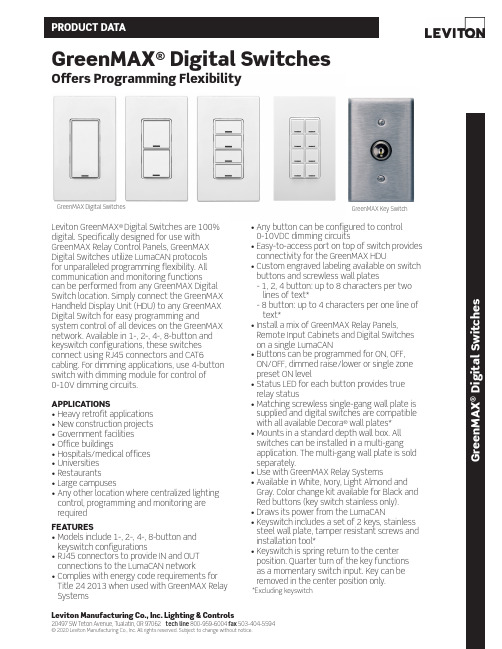
Leviton Manufacturing Co., Inc. Lighting & Controls20497 SW Teton Avenue, Tualatin, OR 97062 tech line 800-959-6004 fax 503-404-5594© 2020 Leviton Manufacturing Co., Inc. All rights reserved. Subject to change without notice.G r e e n M A X ®D i g i t a l S w i t c h e sGreenMAX® Digital Switches Offers Programming FlexibilityLeviton GreenMAX® Digital Switches are 100% digital. Specifically designed for use with GreenMAX Relay Control Panels, GreenMAX Digital Switches utilize LumaCAN protocolsfor unparalleled programming flexibility. All communication and monitoring functionscan be performed from any GreenMAX Digital Switch location. Simply connect the GreenMAX Handheld Display Unit (HDU) to any GreenMAX Digital Switch for easy programming and system control of all devices on the GreenMAX network. Available in 1-, 2-, 4-, 8-button and keyswitch configurations, these switches connect using RJ45 connectors and CAT6 cabling. For dimming applications, use 4-button switch with dimming module for control of0-10V dimming circuits.APPLICATIONS• Heavy retrofit applications• New construction projects• Government facilities• Office buildings• Hospitals/medical offices• Universities• Restaurants• Large campuses• Any other location where centralized lighting control, programming and monitoring are requiredFEATURES• Models include 1-, 2-, 4-, 8-button and keyswitch configurations• RJ45 connectors to provide IN and OUT connections to the LumaCAN network• Complies with energy code requirements for Title 24 2013 when used with GreenMAX Relay Systems • Any button can be configured to control0-10VDC dimming circuits• Easy-to-access port on top of switch provides connectivity for the GreenMAX HDU• Custom engraved labeling available on switch buttons and screwless wall plates- 1, 2, 4 button: up to 8 characters per two lines of text*- 8 button: up to 4 characters per one line of text*• Install a mix of GreenMAX Relay Panels, Remote Input Cabinets and Digital Switches on a single LumaCAN• Buttons can be programmed for ON, OFF, ON/OFF, dimmed raise/lower or single zone preset ON level• Status LED for each button provides true relay status• Matching screwless single-gang wall plate is supplied and digital switches are compatible with all available Decora® wall plates*• Mounts in a standard depth wall box. All switches can be installed in a multi-gang application. The multi-gang wall plate is sold separately.• Use with GreenMAX Relay Systems• Available in White, Ivory, Light Almond and Gray. Color change kit available for Black and Red buttons (key switch stainless only).• Draws its power from the LumaCAN• Keyswitch includes a set of 2 keys, stainless steel wall plate, tamper resistant screws and installation tool*• Keyswitch is spring return to the center position. Quarter turn of the key functionsas a momentary switch input. Key can be removed in the center position only.*Excluding keyswitchGreenMAX Key SwitchGreenMAX Digital SwitchesPRODUCT DATASPECIFICATIONSElectrical• Input Power: 24VDC (LumaCAN integral)• Consumption: 1 Unit Load = 25mA (max)• Connectors: RJ45• Class 2• Cables: Cat6Environmental• Ambient Temperature Range: 32 - 122°F (0 - 50°C)• Relative Humidity: <90% non-condensingListings• Complies with energy code requirements for ASHRAE Standard 90.1 2010 and Title 24 2013 Warranty• Limited 2-Year WarrantyDIMENSIONS1,2,4,8 Button SwitchesKeyswitch A 1.65” (42.06mm) 1.70” (43.18mm)B4.60” (117.07mm) 4.50” (114.30mm)C 2.75” (69.85mm) 2.75” (69.85mm)D 0.37” (9.55mm)0.28” (7.21mm)E1.16” (29.51mm) 1.88” (47.88mm)F2.68” (68.25mm)2.70” (68.58mm)WIRING DIAGRAM * Replace x to indicate color: (W) = White, (I) = Ivory, (T) = Light Almond, (G) = GrayReplace y to indicate color: (W) = White, (I) = Ivory, (T) = Light Almond, (G) = Gray (R) = Red, (E) = Black ** Stainless steel wallplate cannot be engraved. Multi-gang keyswitch order requires a custom wallplateG-8320F/L19-AJAREV DEC 2019Leviton Manufacturing Co., Inc. Lighting & Controls20497 SW Teton Avenue, Tualatin, OR 97062 tel 800-736-6682 fax 503-404-5594 tech line (6:00AM-4:00PM PT Mon-Fri) 800-959-6004Leviton Manufacturing Co., Inc. Global Headquarters201 North Service Road, Melville, NY 11747-3138 tel 800-323-8920 fax 800-832-9538 tech line (8:30AM-7:00PM ET Mon-Fri) 800-824-3005Visit our Website at: /greenmax©2020 Leviton Manufacturing Co., Inc. All rights reserved. Subject to change without notice.。

___________________________________________________________________Selector Guide________________General DescriptionThe MAX6316–MAX6322 family of microprocessor (µP)supervisory circuits monitors power supplies and microprocessor activity in digital systems. It offers sev-eral combinations of push/pull, open-drain, and bidirec-tional (such as Motorola 68HC11) reset outputs, along with watchdog and manual reset features. The Selector Guide below lists the specific functions available from each device. These devices are specifically designed to ignore fast negative transients on V CC . Resets are guaranteed valid for V CC down to 1V.These devices are available in 26 factory-trimmed reset threshold voltages (from 2.5V to 5V, in 100mV incre-ments), featuring four minimum power-on reset timeout periods (from 1ms to 1.12s), and four watchdog timeout periods (from 6.3ms to 25.6s). Thirteen standard ver-sions are available with an order increment requirement of 2500 pieces (see Standard Versions table); contact the factory for availability of other versions, which have an order increment requirement of 10,000 pieces.The MAX6316–MAX6322 are offered in a miniature 5-pin SOT23 package.________________________ApplicationsPortable Computers Computers ControllersIntelligent InstrumentsPortable/Battery-Powered Equipment Embedded Control Systems____________________________Features♦Small 5-Pin SOT23 Package♦Available in 26 Reset Threshold Voltages2.5V to 5V, in 100mV Increments ♦Four Reset Timeout Periods1ms, 20ms, 140ms, or 1.12s (min)♦Four Watchdog Timeout Periods6.3ms, 102ms, 1.6s, or 25.6s (typ) ♦Four Reset Output StagesActive-High, Push/Pull Active-Low, Push/Pull Active-Low, Open-Drain Active-Low, Bidirectional♦Guaranteed Reset Valid to V CC = 1V♦Immune to Short Negative V CC Transients ♦Low Cost♦No External ComponentsMAX6316–MAX63225-Pin µP Supervisory Circuits withWatchdog and Manual Reset________________________________________________________________Maxim Integrated Products 119-0496; Rev 7; 11/07_______________Ordering InformationOrdering Information continued at end of data sheet.*The MAX6318/MAX6319/MAX6321/MAX6322 feature two types of reset output on each device.Typical Operating Circuit and Pin Configurations appear at end of data sheet.For pricing, delivery, and ordering information, please contact Maxim Direct at 1-888-629-4642,or visit Maxim’s website at .Specify lead-free by replacing “-T” with “+T” when ordering.ELECTRICAL CHARACTERISTICS(V CC = 2.5V to 5.5V, T A = -40°C to +125°C, unless otherwise noted. Typical values are at T A = +25°C.) (Note 1)M A X 6316–M A X 63225-Pin µP Supervisory Circuits with Watchdog and Manual Reset 2_______________________________________________________________________________________ABSOLUTE MAXIMUM RATINGSStresses beyond those listed under “Absolute Maximum Ratings” may cause permanent damage to the device. These are stress ratings only, and functional operation of the device at these or any other conditions beyond those indicated in the operational sections of the specifications is not implied. Exposure to absolute maximum rating conditions for extended periods may affect device reliability.Voltage (with respect to GND)V CC ......................................................................-0.3V to +6V RESET (MAX6320/MAX6321/MAX6322 only)...... -0.3V to +6V All Other Pins.........................................-0.3V to (V CC + 0.3V)Input/Output Current, All Pins.............................................20mAContinuous Power Dissipation (T A = +70°C)SOT23-5 (derate 7.1mW/°C above +70°C)...............571mW Operating Temperature Range..........................-40°C to +125°C Junction Temperature......................................................+150°C Storage Temperature Range..............................-65°C to +160°C Lead Temperature (soldering, 10s).................................+300°CTH available in 100mV increments from 2.5V to 5V (see Table 1 at end of data sheet).Note 3:Guaranteed by design.MAX6316–MAX63225-Pin µP Supervisory Circuits withWatchdog and Manual Reset_______________________________________________________________________________________3Note 5:Measured from RESET V OL to (0.8 x V CC ), R LOAD = ∞.Note 6:WDI is internally serviced within the watchdog period if WDI is left unconnected.Note 7:The WDI input current is specified as the average input current when the WDI input is driven high or low. The WDI input is designed for a three-stated-output device with a 10µA maximum leakage current and capable of driving a maximum capac-itive load of 200pF. The three-state device must be able to source and sink at least 200µA when active.ELECTRICAL CHARACTERISTICS (continued)M A X 6316–M A X 63225-Pin µP Supervisory Circuits with Watchdog and Manual Reset 4_________________________________________________________________________________________________________________________________Typical Operating Characteristics(T A = +25°C, unless otherwise noted.)021*********-4020-20406080100MAX6316/MAX6317/MAX6318/MAX6320/MAX6321SUPPLY CURRENT vs. TEMPERATURETEMPERATURE (°C)S U P P L Y C U R R E N T (μA )302010504090807060100-40-20020406080100V CC FALLING TO RESET PROPAGATIONDELAY vs. TEMPERATURETEMPERATURE (°C)R E S E T P R O P A G A T I O N D E L A Y (μs )140180160240220200300280260320-40020-20406080100MAX6316/MAX6317/MAX6319/MAX6320/MAX6322MANUAL RESET TO RESETPROPAGATION DELAY vs. TEMPERATURETEMPERATURE (°C)P R O P A G A T I O N D E L A Y (n s )0.950.980.970.961.000.991.041.031.021.011.05-40-2020406080100NORMALIZED RESET TIMEOUT PERIOD vs. TEMPERATUREM A X 6316t o c 04TEMPERATURE (°C)N O R M A L I Z E D R E S E T T I M E O U T P E R I O D0.950.980.970.961.000.991.041.031.021.011.05-40-2020406080100MAX6316/MAX6317/MAX6318/MAX6320/MAX6321NORMALIZED WATCHDOG TIMEOUTPERIOD vs. TEMPERATUREM A X 6316t o c 05TEMPERATURE (°C)N O R M A L I Z E D W A T C H D O G T I M E O U T P E R I O D800101001000MAXIMUM V CC TRANSIENT DURATION vs. RESET THRESHOLD OVERDRIVE2010RESET THRESHOLD OVERDRIVE (mV) V RST - V CCT RA N S I E N T D U R A T I O N (μs )3050604070200ns/divMAX6316M/6318MH/6319MHBIDIRECTIONALPULLUP CHARACTERISTICSMAX6316–MAX63225-Pin µP Supervisory Circuits withWatchdog and Manual Reset_______________________________________________________________________________________5______________________________________________________________Pin DescriptionM A X 6316–M A X 63225-Pin µP Supervisory Circuits with Watchdog and Manual Reset 6______________________________________________________________________________________________________Detailed DescriptionA microprocessor’s (µP) reset input starts or restarts the µP in a known state. The reset output of the MAX6316–MAX6322 µP supervisory circuits interfaces with the reset input of the µP, preventing code-execution errors during power-up, power-down, and brownout condi-tions (see the Typical Operating Circuit ). The MAX6316/MAX6317/MAX6318/MAX6320/MAX6321 are also capa-ble of asserting a reset should the µP become stuck in an infinite loop.Reset OutputThe MAX6316L/MAX6318LH/MAX6319LH feature an active-low reset output, while the MAX6317H/MAX6318_H/MAX6319_H/MAX6321HP/MAX6322HP feature an active-high reset output. RESET is guaran-teed to be a logic low and RESET is guaranteed to be a logic high for V CC down to 1V.The MAX6316–MAX6322 assert reset when V CC is below the reset threshold (V RST ), when MR is pulled low (MAX6316_/MAX6317H/MAX6319_H/MAX6320P/MAX6322HP only), or if the WDI pin is not serviced withinthe watchdog timeout period (t WD ). Reset remains assert-ed for the specified reset active timeout period (t RP ) after V CC rises above the reset threshold, after MR transitions low to high, or after the watchdog timer asserts the reset (MAX6316_/MAX6317H/MAX6318_H/MAX6320P/MAX6321HP). After the reset active timeout period (t RP )expires, the reset output deasserts, and the watchdog timer restarts from zero (Figure 2).Figure 1. Functional DiagramFigure 2. Reset Timing DiagramMAX6316–MAX63225-Pin µP Supervisory Circuits withWatchdog and Manual Reset_______________________________________________________________________________________7Bidirectional R E S E T OutputThe MAX6316M/MAX6318MH/MAX6319MH are designed to interface with µPs that have bidirectional reset pins,such as the Motorola 68HC11. Like an open-drain output,these devices allow the µP or other devices to pull the bidirectional reset (RESET ) low and assert a reset condi-tion. However, unlike a standard open-drain output, it includes the commonly specified 4.7k Ωpullup resistor with a P-channel active pullup in parallel.This configuration allows the MAX6316M/MAX6318MH/MAX6319MH to solve a problem associated with µPs that have bidirectional reset pins in systems where sev-eral devices connect to RESET (F igure 3). These µPs can often determine if a reset was asserted by an exter-nal device (i.e., the supervisor IC) or by the µP itself (due to a watchdog fault, clock error, or other source),and then jump to a vector appropriate for the source of the reset. However, if the µP does assert reset, it does not retain the information, but must determine the cause after the reset has occurred.The following procedure describes how this is done in the Motorola 68HC11. In all cases of reset, the µP pulls RESET low for about four external-clock cycles. It then releases RESET , waits for two external-clock cycles,then checks RESET ’s state. If RESET is still low, the µP concludes that the source of the reset was external and, when RESET eventually reaches the high state, it jumps to the normal reset vector. In this case, stored-state information is erased and processing begins fromscratch. If, on the other hand, RESET is high after a delay of two external-clock cycles, the processor knows that it caused the reset itself and can jump to a different vector and use stored-state information to determine what caused the reset.A problem occurs with faster µPs; two external-clock cycles are only 500ns at 4MHz. When there are several devices on the reset line, and only a passive pullup resis-tor is used, the input capacitance and stray capacitance can prevent RESET from reaching the logic high state (0.8✕V CC ) in the time allowed. If this happens, all resets will be interpreted as external. The µP output stage is guaran-teed to sink 1.6mA, so the rise time can not be reduced considerably by decreasing the 4.7k Ωinternal pullup resistance. See Bidirectional Pullup Characteristics in the Typical Operating Characteristics .The MAX6316M/MAX6318MH/MAX6319MH overcome this problem with an active pullup FET in parallel with the 4.7k Ωresistor (F igures 4 and 5). The pullup transistor holds RESET high until the µP reset I/O or the supervisory circuit itself forces the line low. Once RESET goes below V PTH , a comparator sets the transition edge flip-flop, indi-cating that the next transition for RESET will be low to high. When RESET is released, the 4.7k Ωresistor pulls RESET up toward V CC . Once RESET rises above V PTH but is below (0.85 x V CC ), the active P-channel pullup turns on. Once RESET rises above (0.85 x V CC ) or the 2µs one-shot times out, the active pullup turns off. The parallel combination of the 4.7k Ωpullup and theFigure 3. MAX6316M/MAX6318MH/MAX6319MH Supports Additional Devices on the Reset BusM A X 6316–M A X 63225-Pin µP Supervisory Circuits with Watchdog and Manual Reset 8_______________________________________________________________________________________Figure 4. MAX6316/MAX6318MH/MAX6319MH Bidirectional Reset Output Functional DiagramMAX6316–MAX63225-Pin µP Supervisory Circuits withWatchdog and Manual Reset_______________________________________________________________________________________9P-channel transistor on-resistance quickly charges stray capacitance on the reset line, allowing RESET to transition from low to high within the required two elec-tronic-clock cycles, even with several devices on the reset line. This process occurs regardless of whether the reset was caused by V CC dipping below the reset threshold, the watchdog timing out, MR being asserted,or the µP or other device asserting RESET . The parts do not require an external pullup. To minimize supply cur-rent consumption, the internal 4.7k Ωpullup resistor dis-connects from the supply whenever the MAX6316M/MAX6318MH/MAX6319MH assert reset.Open-Drain R E S E T OutputThe MAX6320P/MAX6321HP/MAX6322HP have an active-low, open-drain reset output. This output struc-ture will sink current when RESET is asserted. Connect a pullup resistor from RESET to any supply voltage up to 6V (Figure 6). Select a resistor value large enough toregister a logic low (see Electrical Characteristics ), and small enough to register a logic high while supplying all input current and leakage paths connected to the RESET line. A 10k Ωpullup is sufficient in most applications.Manual-Reset InputThe MAX6316_/MAX6317H/MAX6319_H/MAX6320P/MAX6322HP feature a manual reset input. A logic low on MR asserts a reset. After MR transitions low to high, reset remains asserted for the duration of the reset timeout peri-od (t RP ). The MR input is connected to V CC through an internal 52k Ωpullup resistor and therefore can be left unconnected when not in use. MR can be driven with TTL-logic levels in 5V systems, with CMOS-logic levels in 3V systems, or with open-drain or open-collector output devices. A normally-open momentary switch from MR to ground can also be used; it requires no external debouncing circuitry. MR is designed to reject fast, negative-going transients (typically 100ns pulses). A 0.1µF capacitor from MR to ground provides additional noise immunity.The MR input pin is equipped with internal ESD-protection circuitry that may become forward biased. Should MR be driven by voltages higher than V CC , excessive current would be drawn, which would damage the part. F or example, assume that MR is driven by a +5V supply other than V CC . If V CC drops lower than +4.7V, MR ’s absolute maximum rating is violated [-0.3V to (V CC + 0.3V)], and undesirable current flows through the ESD structure from MR to V CC . To avoid this, use the same supply for MR as the supply monitored by V CC . This guarantees that the voltage at MR will never exceed V CC .Watchdog InputThe MAX6316_/MAX6317H/MAX6318_H/MAX6320P/MAX6321HP feature a watchdog circuit that monitors the µP’s activity. If the µP does not toggle the watchdog input (WDI) within the watchdog timeout period (t WD ),reset asserts. The internal watchdog timer is cleared by reset or by a transition at WDI (which can detect pulses as short as 50ns). The watchdog timer remains cleared while reset is asserted. Once reset is released, the timer begins counting again (Figure 7).The WDI input is designed for a three-stated output device with a 10µA maximum leakage current and the capability of driving a maximum capacitive load of 200pF.The three-state device must be able to source and sink at least 200µA when active. Disable the watchdog function by leaving WDI unconnected or by three-stating the driver connected to WDI. When the watchdog timer is left open circuited, the timer is cleared internally at intervals equal to 7/8 of the watchdog period.Figure 6. MAX6320P/MAX6321HP/MAX6322HP Open-Drain RESET Output Allows Use with Multiple SuppliesFigure 5. Bidirectional RESET Timing DiagramM A X 6316–M A X 63225-Pin µP Supervisory Circuits with Watchdog and Manual Reset 10______________________________________________________________________________________Applications InformationWatchdog Input CurrentThe WDI input is internally driven through a buffer and series resistor from the watchdog counter. For minimum watchdog input current (minimum overall power con-sumption), leave WDI low for the majority of the watch-dog timeout period. When high, WDI can draw as much as 160µA. Pulsing WDI high at a low duty cycle will reduce the effect of the large input current. When WDI is left unconnected, the watchdog timer is serviced within the watchdog timeout period by a low-high-low pulse from the counter chain.Negative-Going V CC TransientsThese supervisors are immune to short-duration, nega-tive-going V CC transients (glitches), which usually do not require the entire system to shut down. Typically,200ns large-amplitude pulses (from ground to V CC ) on the supply will not cause a reset. Lower amplitude puls-es result in greater immunity. Typically, a V CC transient that goes 100mV under the reset threshold and lasts less than 4µs will not trigger a reset. An optional 0.1µF bypass capacitor mounted close to V CC provides addi-tional transient immunity.Ensuring Valid Reset OutputsDown to V CC = 0The MAX6316_/MAX6317H/MAX6318_H/MAX6319_H/MAX6321HP/MAX6322HP are guaranteed to operate properly down to V CC = 1V. In applications that require valid reset levels down to V CC = 0, a pulldown resistor to active-low outputs (push/pull and bidirectional only,F igure 8) and a pullup resistor to active-high outputs(push/pull only, Figure 9) will ensure that the reset line is valid while the reset output can no longer sink orsource current. This scheme does not work with the open-drain outputs of the MAX6320/MAX6321/MAX6322.The resistor value used is not critical, but it must be large enough not to load the reset output when V CC is above the reset threshold. F or most applications,100k Ωis adequate.Watchdog Software Considerations(MAX6316/MAX6317/MAX6318/MAX6320/MAX6321)One way to help the watchdog timer monitor software execution more closely is to set and reset the watchdog input at different points in the program, rather than pulsing the watchdog input high-low-high or low-high-low. This technique avoids a stuck loop, in which the watchdog timer would continue to be reset inside the loop, keeping the watchdog from timing out.Figure 7. Watchdog Timing RelationshipFigure 9. Ensuring RESET Valid to V CC = 0 on Active-High Push/Pull OutputsFigure 8. Ensuring RESET Valid to V CC = 0 on Active-Low Push/Pull and Bidirectional OutputsMAX6316–MAX6322Watchdog and Manual Reset______________________________________________________________________________________11F igure 10 shows an example of a flow diagram where the I/O driving the watchdog input is set high at the beginning of the program, set low at the end of every subroutine or loop, then set high again when the pro-gram returns to the beginning. If the program should hang in any subroutine, the problem would be quickly corrected, since the I/O is continually set low and the watchdog timer is allowed to time out, causing a reset or interrupt to be issued. As described in the Watchdog Input Current section, this scheme results in higher time average WDI current than does leaving WDI low for the majority of the timeout period and periodically pulsing it low-high-low.Figure 10. Watchdog Flow Diagram__________________Pin ConfigurationsTypical Operating CircuitTable 2. Standard VersionsTable 1. Factory-Trimmed Reset ThresholdsM A X 6316–M A X 6322Watchdog and Manual ResetTable 3. Reset/Watchdog Timeout PeriodsMAX6316–MAX6322Watchdog and Manual Reset______________________________________________________________________________________13__Ordering Information (continued)a watchdog feature (see Selector Guide) are factory-trimmed to one of four watchdog timeout periods. Insert the letter corre-sponding to the desired watchdog timeout period (W, X, Y, or Z from Table 3) into the blank following the reset timeout suffix.TRANSISTOR COUNT: 191SUBSTRATE IS INTERNALLY CONNECTED TO V+Chip Informationdard versions only. The required order increment for nonstandard versions is 10,000 pieces. Contact factory for availability.M A X 6316–M A X 6322Watchdog and Manual Reset 14______________________________________________________________________________________Package Information(The package drawing(s) in this data sheet may not reflect the most current specifications. For the latest package outline information,go to /packages .)M axim cannot assume responsibility for use of any circuitry other than circuitry entirely embodied in a M axim product. No circuit patent licenses are implied. Maxim reserves the right to change the circuitry and specifications without notice at any time.Maxim Integrated Products, 120 San Gabriel Drive, Sunnyvale, CA 94086 408-737-7600 ____________________15©2007 Maxim Integrated Productsis a registered trademark of Maxim Integrated Products, Inc.MAX6316–MAX6322 Watchdog and Manual ResetRevision History。


For free samples & the latest literature: , or phone 1-800-998-8800.For small orders, phone 408-737-7600 ext. 3468.General DescriptionThe MAX6305–MAX6313 CMOS microprocessor (µP)supervisory circuits are designed to monitor more than one power supply. Ideal for monitoring both 5V and 3.3V in personal computer systems, these devicesFeatureso Small 5-Pin SOT23 Packageo Precision Factory-Set V CC Reset Thresholds;Available in 0.1V Increments from 2.5V to 5V o Immune to Short V TransientsMAX6305–MAX63135-Pin, Multiple-Input,Programmable Reset ICs________________________________________________________________Maxim Integrated Products 119-1145; Rev 1; 8/98M A X 6305–M A X 63135-Pin, Multiple-Input, Programmable Reset ICs 2_______________________________________________________________________________________ABSOLUTE MAXIMUM RATINGSELECTRICAL CHARACTERISTICSV CC = +2.5V to +5.5V for the MAX6305/MAX6308/MAX6311, V CC = (V TH + 2.5%) to +5.5V for the MAX6306/MAX6307/MAX6309/MAX6310/MAX6312/MAX6313; T A = 0°C to +70°C; unless otherwise noted. Typical values are at T A = +25°C.)Stresses beyond those listed under “Absolute Maximum Ratings” may cause permanent damage to the device. These are stress ratings only, and functional operation of the device at these or any other conditions beyond those indicated in the operational sections of the specifications is not implied. Exposure to absolute maximum rating conditions for extended periods may affect device reliability.V CC ...........................................................................-0.3V to +6V All Other Pins..............................................-0.3V to (V CC + 0.3V)Input/Output Current, All Pins.............................................20mA Rate of Rise, V CC ............................................................100V/µsContinuous Power Dissipation (T A = +70°C)SOT23-5 (derate 7.1mW/°C above +70°C).................571mW Operating Temperature Range...............................0°C to +70°C Storage Temperature Range.............................-65°C to +160°C Lead Temperature (soldering, 10sec).............................+300°CMAX6305–MAX63135-Pin, Multiple-Input, Programmable Reset ICs_______________________________________________________________________________________3ELECTRICAL CHARACTERISTICS (continued)(V CC = +2.5V to +5.5V for the MAX6305/MAX6308/MAX6311, V CC = (V TH + 2.5%) to +5.5V for the MAX6306/MAX6307/MAX6309/MAX6310/MAX6312/MAX6313; T A = 0°C to +70°C; unless otherwise noted. Typical values are at T A = +25°C.)Note 1: The MAX6305/MAX6308/MAX6311 switch from undervoltage reset to normal operation between 1.5V < V CC < 2.5V.Note 2: The MAX6306/MAX6307/MAX6309/MAX6310/MAX6312/MAX6313 monitor V CC through an internal factory-trimmed voltagedivider, which programs the nominal reset threshold. Factory-trimmed reset thresholds are available in approximately 100mV increments from 2.5V to 5V (Table 1).M A X 6305–M A X 63135-Pin, Multiple-Input, Programmable Reset ICs 4_________________________________________________________________________________________________________________________________Typical Operating Characteristics(V CC = +5V, T A = +25°C, unless otherwise noted.)5.05.56.06.57.07.58.08.59.09.5-60-40-2020406080100SUPPLY CURRENT vs. TEMPERATURETEMPERATURE (°C)S U P P L Y C U R R E N T (µA )01020304050607080-60-40-2020406080100V CC FALLING PROPAGATION DELAYvs. TEMPERATURETEMPERATURE (°C)P R O P A G A T I O N D E L A Y (n s )010203040506070-60-40-20020406080100OVRST IN RISING PROPAGATION DELAY vs. TEMPERATURE (OVERVOLTAGE RESET INPUT)TEMPERATURE (°C)P R O P A G A T I O N D E L A Y (n s )020406080100120-60-40-2020406080100RST IN_ FALLING PROPAGATION DELAY vs. TEMPERATURETEMPERATURE (°C)R S T I N _ P R O P A G A T I O N D E L A Y (n s )104001200800MAXIMUM TRANSIENT DURATION vs.V CC RESET THRESHOLD OVERDRIVE10OVERDRIVE, V TH - V CC (mV)T R A N S I E N T D U R A T I O N (µs )100100010,0000.900.920.940.960.981.001.021.041.061.081.10-60-40-20020406080100RESET TIMEOUT vs. TEMPERATURE6305 T O C 05TEMPERATURE (°C)N O R M A L I Z E D R E S E T T I M E O U T0.9900.9920.9940.9960.9981.0001.0021.0041.0061.0081.010-60-40-2020406080100RESET THRESHOLD vs. TEMPERATURE6305 T O C 06TEMPERATURE (°C)N O R M A L I Z E D R E S E T T H R E S H O L D (V /V )104001200800MAXIMUM TRANSIENT DURATION vs.OVRST IN THRESHOLD OVERDRIVE10OVERDRIVE, V OVRST IN - V REF (mV)T R A N S I E N T D U R A T I O N (µs )100100010,000104001200800MAXIMUM TRANSIENT DURATION vs.RST IN_ THRESHOLD OVERDRIVE10OVERDRIVE, V REF - V RST IN (mV)T R A N S I E N T D U R A T I O N (µs )100100010,000_______________Detailed DescriptionThe MAX6305–MAX6313 CMOS microprocessor (µP)supervisory circuits are designed to monitor more than one power supply and issue a system reset when any monitored supply falls out of regulation. The MAX6305/MAX6308/MAX6311 have two adjustable undervoltage reset inputs (RST IN1 and RST IN2). The MAX6306/MAX6307/MAX6309/MAX6310/MAX6312/MAX6313 mon-itor V CC through an internal, factory-trimmed voltage divider. The MAX6306/MAX6309/MAX6312 have, in addition, an adjustable undervoltage reset input and a manual-reset input. The internal voltage divider sets the reset threshold as specified in the device part number (Table 1). The MAX6307/MAX6310/ MAX6313 feature an adjustable undervoltage reset input (RST IN) and an adjustable overvoltage reset input (OVRST IN) in addition to the factory-trimmed reset threshold on the V CC moni-tor. Program the adjustable reset inputs with an external resistor divider (see Adjustable Reset Inputs section).Reset OutputsA µP’s reset input starts the µP in a known state. These µP supervisory circuits assert reset to prevent code-execution errors during power-up, power-down, or brownout conditions.RESET (MAX6305–MAX6310) and RESET (MAX6311/MAX6312/MAX6313) are guaranteed to be asserted at a valid logic level for V CC > 1V (see Electrical Characteristics ). Once all monitored voltages exceed their programmed reset thresholds, an internal timer keeps reset asserted for the reset timeout period (t RP );after this interval, reset deasserts.If a brownout condition occurs (any or all monitored volt-ages dip outside their programmed reset threshold),reset asserts (RESET goes high; RESET goes low). Any time any of the monitored voltages dip below their reset threshold, the internal timer resets to zero and reset asserts. The internal timer starts when all of the moni-tored voltages return above their reset thresholds, and reset remains asserted for a reset timeout period. The MAX6305/MAX6306/MAX6307 feature an active-low,MAX6305–MAX63135-Pin, Multiple-Input, Programmable Reset ICs_______________________________________________________________________________________5______________________________________________________________Pin DescriptionM A X 6305–M A X 6313open-drain, N-channel output. The MAX6308/MAX6309/MAX6310 feature an active-low, complementary output structure that both sinks and sources current, and the MAX6311/MAX6312/MAX6313 have an active-high com-plementary reset output.The MAX6305/MAX6308/MAX6311 switch from under-voltage lockout operation to normal operation between 1.5V < V CC < 2.5V. Below 1.5V, V CC undervoltage-lockout mode asserts RESET . Above 2.5V, V CC normal-operation mode asserts reset if RST IN_ falls below the RST IN_ threshold.Manual-Reset Input(MAX6306/MAX6309/MAX6312)Many µP-based products require manual-reset capability,allowing an operator or external logic circuitry to initiate a reset. A logic low on MR asserts reset. Reset remains asserted while MR is low, and for a reset active timeout period (t RP ) after MR returns high. This input has an inter-nal 63.5k Ωpull-up resistor, so it can be left open if it is not used. MR can be driven with TTL-logic levels in 5V sys-tems, with CMOS-logic levels in 3V systems, or with open-drain/collector output devices. Connect a normally open momentary switch from MR to GND to create a manual-reset function; external debounce circuitry is not required.If MR is driven from long cables or if the device is used in a noisy environment, connecting a 0.1µF capacitor from MR to ground provides additional noise immunity.The MR pin has internal ESD-protection circuitry that may be forward biased under certain conditions, drawing excessive current. For example, assume the circuitry driv-ing MR uses a +5V supply other than V CC . If V CC drops or browns out lower than +4.7V, MR ’s absolute maximum rat-ing is violated (-0.3V to (V CC + 0.3V)), and undesirable current flows through the ESD structure from MR to V CC .To avoid this, it is recommended that the supply for the MR pin be the same as the supply monitored by V CC . In this way, the voltage at MR will not exceed V CC .Adjustable Reset InputsThe MAX6305–MAX6313 each have one or more reset inputs (RST IN_ /OVRST IN). These inputs are com-pared to the internal reference voltage (Figure 1).Connect a resistor voltage divider to RST IN_ such that V RST IN_falls below V RSTH (1.23V) when the monitored voltage (V IN ) falls below the desired reset threshold (V TH ) (Figure 2). Calculate the desired reset voltage with the following formula:R1 + R2V TH = ________x V RSTHR25-Pin, Multiple-Input, Programmable Reset ICs 6_______________________________________________________________________________________Figure 1. Functional DiagramMAX6305–MAX63135-Pin, Multiple-Input, Programmable Reset ICs_______________________________________________________________________________________7The ±25nA max input leakage current allows resistors on the order of megohms. Choose the pull-up resistor in the divider to minimize the error due to the input leakage cur-rent. The error term in the calculated threshold is simply:±25nA x R1If you choose R1 to be 1M Ω, the resulting error is ±25 x 10-9x 1 x 106= ±25mV.Like the V CC voltage monitors on the MAX6306/MAX6307/MAX6309/MAX6310/MAX6312/MAX6313, the RST IN_inputs (when used with a voltage divider) are designed to ignore fast voltage transients. Increase the noise immunity by connecting a capacitor on the order of 0.1µF between RST IN and GND (Figure 2). This creates a single-pole lowpass filter with a corner frequency given by:f = (1/2π) / (R1 + R2)(R1 x R2 x C)For example, if R1 = 1M Ωand R2 = 1.6M Ω, adding a 0.1µF capacitor from RST IN_ to ground results in a lowpass corner frequency of f = 2.59Hz. Note that adding capacitance to RST IN slows the circuit’s overall response time.__________Applications InformationInterfacing to µPs with Bidirectional Reset PinsSince the RESET output on the MAX6305/MAX6306/MAX6307 is open drain, these devices interface easily with µPs that have bidirectional reset pins, such as the Motorola 68HC11. Connecting the µP supervisor’s RESET output directly to the microcontroller’s RESET pin with a single pull-up resistor allows either device to assert reset (Figure 3).Negative-Going V CC TransientsIn addition to issuing a reset to the µP during power-up,power-down, and brownout conditions, these devices are relatively immune to short-duration, negative-going V CC transients (glitches).The Typical Operating Characteristics show the Maximum Transient Duration vs. V CC Reset Threshold Overdrive, for which reset pulses are not generated.The graph was produced using negative-going pulses,starting at V TH max, and ending below the pro-grammed reset threshold by the magnitude indicated (reset threshold overdrive). The graph shows the maxi-mum pulse width that a negative-going V CC transient may typically have without causing a reset pulse to be issued. As the amplitude of the transient increases (i.e.,goes farther below the reset threshold), the maximum allowable pulse width decreases.RST IN_/OVRST IN are also immune to negative/positive-going transients (see Typical Operating Characteristics ).A 0.1µF bypass capacitor mounted close to the RST IN_,OVRST IN, and/or the V CC pin provides additional tran-sient immunity.Ensuring a Valid RESET /RESETOutput Down to V CC = 0VWhen V CC falls below 1V, push/pull structured RESET /RESET current sinking (or sourcing) capabilities decrease drastically. High-impedance CMOS-logic inputs connected to RESET can drift to undetermined voltages. This presents no problem in most applica-tions, since most µPs and other circuitry do not operate with V CC below 1V. In those applications where RESET must be valid down to 0V, adding a pull-down resistor between RESET and ground sinks any stray leakageFigure 2. Increasing Noise ImmunityFigure 3. Interfacing to µPs with Bidirectional Reset I/Ocurrents, holding RESET low (Figure 4). The pull-down resistor’s value is not critical; 100k Ωis large enough not to load RESET and small enough to pull RESET to ground. For applications where RESET must be valid to V CC , a 100k Ωpull-up resistor between RESET and V CC will hold RESET high when V CC falls below 1V (Figure 5).Since the MAX6305/MAX6306/MAX6307 have open-drain, active-low outputs, they typically use a pull-up resistor. With these devices and under these conditions (V CC < 1V), RESET will most likely not maintain an active condition, but will drift toward a nonactive level due to the pull-up resistor and the RESET output’s reduction in sinking capability. These devices are not recommended for applications that require a valid RESET output below 1V.* Factory-trimmed reset thresholds are available in approximately 100mV increments with a ±1.5% room-temperature variance.M A X 6305–M A X 63135-Pin, Multiple-Input, Programmable Reset ICs 8_______________________________________________________________________________________Figure 4. Ensuring RESET Valid to V CC = 0VFigure 5. Ensuring RESET Valid to V CC = 0VTable 1. Factory-Trimmed Reset Thresholds *MAX6305UK00D1-T ABAK MAX6306UK41D3-T ABCA MAX6306UK30D1-T ABDQ MAX6307UK46D3-T ABFG MAX6305UK00D2-T ABAL MAX6306UK41D4-T ABCB MAX6306UK30D2-T ABDR MAX6307UK46D4-T ABFH MAX6305UK00D3-T ABAM MAX6306UK40D1-T ABCC MAX6306UK30D3-T ABDS MAX6307UK45D1-T ABFI MAX6305UK00D4-T ABAN MAX6306UK40D2-T ABCD MAX6306UK30D4-T ABDT MAX6307UK45D2-T ABFJ MAX6306UK50D1-T ABAO MAX6306UK40D3-T ABCE MAX6306UK29D1-T ABDU MAX6307UK45D3-T ABFK MAX6306UK50D2-T ABAP MAX6306UK40D4-T ABCF MAX6306UK29D2-T ABDV MAX6307UK45D4-T ABFL MAX6306UK50D3-T ABAQ MAX6306UK39D1-T ABCG MAX6306UK29D3-T ABDW MAX6307UK44D1-T ABFM MAX6306UK50D4-T ABAR MAX6306UK39D2-T ABCH MAX6306UK29D4-T ABDX MAX6307UK44D2-T ABFN MAX6306UK49D1-T ABAS MAX6306UK39D3-T ABCI MAX6306UK28D1-T ABDY MAX6307UK44D3-T ABFO MAX6306UK49D2-T ABAT MAX6306UK39D4-T ABCJ MAX6306UK28D2-T ABDZ MAX6307UK44D4-T ABFP MAX6306UK49D3-T ABAU MAX6306UK38D1-T ABCK MAX6306UK28D3-T ABEA MAX6307UK43D1-T ABFQ MAX6306UK49D4-T ABAV MAX6306UK38D2-T ABCL MAX6306UK28D4-T ABEB MAX6307UK43D2-T ABFR MAX6306UK48D1-T ABAW MAX6306UK38D3-T ABCM MAX6306UK27D1-T ABEC MAX6307UK43D3-T ABFS MAX6306UK48D2-T ABAX MAX6306UK38D4-T ABCN MAX6306UK27D2-T ABED MAX6307UK43D4-T ABFT MAX6306UK48D3-T ABAY MAX6306UK37D1-T ABCO MAX6306UK27D3-T ABEE MAX6307UK42D1-T ABFU MAX6306UK48D4-T ABAZ MAX6306UK37D2-T ABCP MAX6306UK27D4-T ABEF MAX6307UK42D2-T ABFV MAX6306UK47D1-T ABBA MAX6306UK37D3-T ABCQ MAX6306UK26D1-T ABEG MAX6307UK42D3-T ABFW MAX6306UK47D2-T ABBB MAX6306UK37D4-T ABCR MAX6306UK26D2-T ABEH MAX6307UK42D4-T ABFX MAX6306UK47D3-T ABBC MAX6306UK36D1-T ABCS MAX6306UK26D3-T ABEI MAX6307UK41D1-T ABFY MAX6306UK47D4-T ABBD MAX6306UK36D2-T ABCT MAX6306UK26D4-T ABEJ MAX6307UK41D2-T ABFZ MAX6306UK46D1-T ABBE MAX6306UK36D3-T ABCU MAX6306UK25D1-T ABEK MAX6307UK41D3-T ABGA MAX6306UK46D2-T ABBF MAX6306UK36D4-T ABCV MAX6306UK25D2-T ABEL MAX6307UK41D4-T ABGB MAX6306UK46D3-T ABBG MAX6306UK35D1-T ABCW MAX6306UK25D3-T ABEM MAX6307UK40D1-T ABGC MAX6306UK46D4-T ABBH MAX6306UK35D2-T ABCX MAX6306UK25D4-T ABEN MAX6307UK40D2-T ABGD MAX6306UK45D1-T ABBI MAX6306UK35D3-T ABCY MAX6307UK50D1-T ABEO MAX6307UK40D3-T ABGE MAX6306UK45D2-T ABBJ MAX6306UK35D4-T ABCZ MAX6307UK50D2-T ABEP MAX6307UK40D4-T ABGF MAX6306UK45D3-T ABBK MAX6306UK34D1-T ABDA MAX6307UK50D3-T ABEQ MAX6307UK39D1-T ABGG MAX6306UK45D4-T ABBL MAX6306UK34D2-T ABDB MAX6307UK50D4-T ABER MAX6307UK39D2-T ABGH MAX6306UK44D1-T ABBM MAX6306UK34D3-T ABDC MAX6307UK49D1-T ABES MAX6307UK39D3-T ABGI MAX6306UK44D2-T ABBN MAX6306UK34D4-T ABDD MAX6307UK49D2-T ABET MAX6307UK39D4-T ABGJ MAX6306UK44D3-T ABBO MAX6306UK33D1-T ABDE MAX6307UK49D3-T ABEU MAX6307UK38D1-T ABGK MAX6306UK44D4-T ABBP MAX6306UK33D2-T ABDF MAX6307UK49D4-T ABEV MAX6307UK38D2-T ABGL MAX6306UK43D1-T ABBQ MAX6306UK33D3-T ABDG MAX6307UK48D1-T ABEW MAX6307UK38D3-T ABGM MAX6306UK43D2-T ABBR MAX6306UK33D4-T ABDH MAX6307UK48D2-T ABEX MAX6307UK38D4-T ABGN MAX6306UK43D3-T ABBS MAX6306UK32D1-T ABDI MAX6307UK48D3-T ABEY MAX6307UK37D1-T ABGO MAX6306UK43D4-T ABBT MAX6306UK32D2-T ABDJ MAX6307UK48D4-T ABEZ MAX6307UK37D2-T ABGP MAX6306UK42D1-T ABBU MAX6306UK32D3-T ABDK MAX6307UK47D1-T ABFA MAX6307UK37D3-T ABGQ MAX6306UK42D2-T ABBV MAX6306UK32D4-T ABDL MAX6307UK47D2-T ABFB MAX6307UK37D4-T ABGR MAX6306UK42D3-T ABBW MAX6306UK31D1-T ABDM MAX6307UK47D3-T ABFC MAX6307UK36D1-T ABGS MAX6306UK42D4-T ABBX MAX6306UK31D2-T ABDN MAX6307UK47D4-T ABFD MAX6307UK36D2-T ABGT MAX6306UK41D1-T ABBY MAX6306UK31D3-T ABDO MAX6307UK46D1-T ABFE MAX6307UK36D3-T ABGU MAX6306UK41D2-TABBZMAX6306UK31D4-TABDPMAX6307UK46D2-TABFFMAX6307UK36D4-TABGVMAX6305–MAX63135-Pin, Multiple-Input, Programmable Reset ICs_______________________________________________________________________________________9Table 2. Device Marking CodesDEVICECODE DEVICECODE DEVICECODE DEVICECODEM A X 6305–M A X 63135-Pin, Multiple-Input, Programmable Reset ICs 10______________________________________________________________________________________Table 2. Device Marking Codes (continued)MAX6307UK35D1-T ABGW MAX6307UK25D3-T ABIM MAX6309UK41D1-T ABKC MAX6309UK31D3-T ABLS MAX6307UK35D2-T ABGX MAX6307UK25D4-T ABIN MAX6309UK41D2-T ABKD MAX6309UK31D4-T ABLT MAX6307UK35D3-T ABGY MAX6308UK00D1-T ABIO MAX6309UK41D3-T ABKE MAX6309UK30D1-T ABLU MAX6307UK35D4-T ABGZ MAX6308UK00D2-T ABIP MAX6309UK41D4-T ABKF MAX6309UK30D2-T ABLV MAX6307UK34D1-T ABHA MAX6308UK00D3-T ABIQ MAX6309UK40D1-T ABKG MAX6309UK30D3-T ABLW MAX6307UK34D2-T ABHB MAX6308UK00D4-T ABIR MAX6309UK40D2-T ABKH MAX6309UK30D4-T ABLX MAX6307UK34D3-T ABHC MAX6309UK50D1-T ABIS MAX6309UK40D3-T ABKI MAX6309UK29D1-T ABLY MAX6307UK34D4-T ABHD MAX6309UK50D2-T ABIT MAX6309UK40D4-T ABKJ MAX6309UK29D2-T ABLZ MAX6307UK33D1-T ABHE MAX6309UK50D3-T ABIU MAX6309UK39D1-T ABKK MAX6309UK29D3-T ABMA MAX6307UK33D2-T ABHF MAX6309UK50D4-T ABIV MAX6309UK39D2-T ABKL MAX6309UK29D4-T ABMB MAX6307UK33D3-T ABHG MAX6309UK49D1-T ABIW MAX6309UK39D3-T ABKM MAX6309UK28D1-T ABMC MAX6307UK33D4-T ABHH MAX6309UK49D2-T ABIX MAX6309UK39D4-T ABKN MAX6309UK28D2-T ABMD MAX6307UK32D1-T ABHI MAX6309UK49D3-T ABIY MAX6309UK38D1-T ABKO MAX6309UK28D3-T ABME MAX6307UK32D2-T ABHJ MAX6309UK49D4-T ABIZ MAX6309UK38D2-T ABKP MAX6309UK28D4-T ABMF MAX6307UK32D3-T ABHK MAX6309UK48D1-T ABJA MAX6309UK38D3-T ABKQ MAX6309UK27D1-T ABMG MAX6307UK32D4-T ABHL MAX6309UK48D2-T ABJB MAX6309UK38D4-T ABKR MAX6309UK27D2-T ABMH MAX6307UK31D1-T ABHM MAX6309UK48D3-T ABJC MAX6309UK37D1-T ABKS MAX6309UK27D3-T ABMI MAX6307UK31D2-T ABHN MAX6309UK48D4-T ABJD MAX6309UK37D2-T ABKT MAX6309UK27D4-T ABMJ MAX6307UK31D3-T ABHO MAX6309UK47D1-T ABJE MAX6309UK37D3-T ABKU MAX6309UK26D1-T ABMK MAX6307UK31D4-T ABHP MAX6309UK47D2-T ABJF MAX6309UK37D4-T ABKV MAX6309UK26D2-T ABML MAX6307UK30D1-T ABHQ MAX6309UK47D3-T ABJG MAX6309UK36D1-T ABKW MAX6309UK26D3-T ABMM MAX6307UK30D2-T ABHR MAX6309UK47D4-T ABJH MAX6309UK36D2-T ABKX MAX6309UK26D4-T ABMN MAX6307UK30D3-T ABHS MAX6309UK46D1-T ABJI MAX6309UK36D3-T ABKY MAX6309UK25D1-T ABMO MAX6307UK30D4-T ABHT MAX6309UK46D2-T ABJJ MAX6309UK36D4-T ABKZ MAX6309UK25D2-T ABMP MAX6307UK29D1-T ABHU MAX6309UK46D3-T ABJK MAX6309UK35D1-T ABLA MAX6309UK25D3-T ABMQ MAX6307UK29D2-T ABHV MAX6309UK46D4-T ABJL MAX6309UK35D2-T ABLB MAX6309UK25D4-T ABMR MAX6307UK29D3-T ABHW MAX6309UK45D1-T ABJM MAX6309UK35D3-T ABLC MAX6310UK50D1-T ABMS MAX6307UK29D4-T ABHX MAX6309UK45D2-T ABJN MAX6309UK35D4-T ABLD MAX6310UK50D2-T ABMT MAX6307UK28D1-T ABHY MAX6309UK45D3-T ABJO MAX6309UK34D1-T ABLE MAX6310UK50D3-T ABMU MAX6307UK28D2-T ABHZ MAX6309UK45D4-T ABJP MAX6309UK34D2-T ABLF MAX6310UK50D4-T ABMV MAX6307UK28D3-T ABIA MAX6309UK44D1-T ABJQ MAX6309UK34D3-T ABLG MAX6310UK49D1-T ABMW MAX6307UK28D4-T ABIB MAX6309UK44D2-T ABJR MAX6309UK34D4-T ABLH MAX6310UK49D2-T ABMX MAX6307UK27D1-T ABIC MAX6309UK44D3-T ABJS MAX6309UK33D1-T ABLI MAX6310UK49D3-T ABMY MAX6307UK27D2-T ABID MAX6309UK44D4-T ABJT MAX6309UK33D2-T ABLJ MAX6310UK49D4-T ABMZ MAX6307UK27D3-T ABIE MAX6309UK43D1-T ABJU MAX6309UK33D3-T ABLK MAX6310UK48D1-T ABNA MAX6307UK27D4-T ABIF MAX6309UK43D2-T ABJV MAX6309UK33D4-T ABLL MAX6310UK48D2-T ABNB MAX6307UK26D1-T ABIG MAX6309UK43D3-T ABJW MAX6309UK32D1-T ABLM MAX6310UK48D3-T ABNC MAX6307UK26D2-T ABIH MAX6309UK43D4-T ABJX MAX6309UK32D2-T ABLN MAX6310UK48D4-T ABND MAX6307UK26D3-T ABII MAX6309UK42D1-T ABJY MAX6309UK32D3-T ABLO MAX6310UK47D1-T ABNE MAX6307UK26D4-T ABIJ MAX6309UK42D2-T ABJZ MAX6309UK32D4-T ABLP MAX6310UK47D2-T ABNF MAX6307UK25D1-T ABIK MAX6309UK42D3-T ABKA MAX6309UK31D1-T ABLQ MAX6310UK47D3-T ABNG MAX6307UK25D2-TABILMAX6309UK42D4-TABKBMAX6309UK31D2-TABLRMAX6310UK47D4-TABNHDEVICECODE DEVICECODE DEVICECODE DEVICECODEMAX6305–MAX6313Programmable Reset ICs______________________________________________________________________________________11Table 2. Device Marking Codes (continued)MAX6310UK46D1-T ABNI MAX6310UK36D3-T ABOY MAX6310UK25D1-T ABQO MAX6312UK42D3-T ABSE MAX6310UK46D2-T ABNJ MAX6310UK36D4-T ABOZ MAX6310UK25D2-T ABQP MAX6312UK42D4-T ABSF MAX6310UK46D3-T ABNK MAX6310UK35D1-T ABPA MAX6310UK25D3-T ABQQ MAX6312UK41D1-T ABSG MAX6310UK46D4-T ABNL MAX6310UK35D2-T ABPB MAX6310UK25D4-T ABQR MAX6312UK41D2-T ABSH MAX6310UK45D1-T ABNM MAX6310UK35D3-T ABPC MAX6311UK00D1-T ABQS MAX6312UK41D3-T ABSI MAX6310UK45D2-T ABNN MAX6310UK35D4-T ABPD MAX6311UK00D2-T ABQT MAX6312UK41D4-T ABSJ MAX6310UK45D3-T ABNO MAX6310UK34D1-T ABPE MAX6311UK00D3-T ABQU MAX6312UK40D1-T ABSK MAX6310UK45D4-T ABNP MAX6310UK34D2-T ABPF MAX6311UK00D4-T ABQV MAX6312UK40D2-T ABSL MAX6310UK44D1-T ABNQ MAX6310UK34D3-T ABPG MAX6311UK50D1-T ABQW MAX6312UK40D3-T ABSM MAX6310UK44D2-T ABNR MAX6310UK34D4-T ABPH MAX6312UK50D2-T ABQX MAX6312UK40D4-T ABSN MAX6310UK44D3-T ABNS MAX6310UK33D1-T ABPI MAX6312UK50D3-T ABQY MAX6312UK39D1-T ABSO MAX6310UK44D4-T ABNT MAX6310UK33D2-T ABPJ MAX6312UK50D4-T ABQZ MAX6312UK39D2-T ABSP MAX6310UK43D1-T ABNU MAX6310UK33D3-T ABPK MAX6312UK49D1-T ABRA MAX6312UK39D3-T ABSQ MAX6310UK43D2-T ABNV MAX6310UK33D4-T ABPL MAX6312UK49D2-T ABRB MAX6312UK39D4-T ABSR MAX6310UK43D3-T ABNW MAX6310UK32D1-T ABPM MAX6312UK49D3-T ABRC MAX6312UK38D1-T ABSS MAX6310UK43D4-T ABNX MAX6310UK32D2-T ABPN MAX6312UK49D4-T ABRD MAX6312UK38D2-T ABST MAX6310UK42D1-T ABNY MAX6310UK32D3-T ABPO MAX6312UK48D1-T ABRE MAX6312UK38D3-T ABSU MAX6310UK42D2-T ABNZ MAX6310UK32D4-T ABPP MAX6312UK48D2-T ABRF MAX6312UK38D4-T ABSV MAX6310UK42D3-T ABOA MAX6310UK31D1-T ABPQ MAX6312UK48D3-T ABRG MAX6312UK37D1-T ABSW MAX6310UK42D4-T ABOB MAX6310UK31D2-T ABPR MAX6312UK48D4-T ABRH MAX6312UK37D2-T ABSX MAX6310UK41D1-T ABOC MAX6310UK31D3-T ABPS MAX6312UK47D1-T ABRI MAX6312UK37D3-T ABSY MAX6310UK41D2-T ABOD MAX6310UK31D4-T ABPT MAX6312UK47D2-T ABRJ MAX6312UK37D4-T ABSZ MAX6310UK41D3-T ABOE MAX6310UK30D1-T ABPU MAX6312UK47D3-T ABRK MAX6312UK36D1-T ABTA MAX6310UK41D4-T ABOF MAX6310UK30D2-T ABPV MAX6312UK47D4-T ABRL MAX6312UK36D2-T ABTB MAX6310UK40D1-T ABOG MAX6310UK30D3-T ABPW MAX6312UK46D1-T ABRM MAX6312UK36D3-T ABTC MAX6310UK40D2-T ABOH MAX6310UK30D4-T ABPX MAX6312UK46D2-T ABRN MAX6312UK36D4-T ABTD MAX6310UK40D3-T ABOI MAX6310UK29D1-T ABPY MAX6312UK46D3-T ABRO MAX6312UK35D1-T ABTE MAX6310UK40D4-T ABOJ MAX6310UK29D2-T ABPZ MAX6312UK46D4-T ABRP MAX6312UK35D2-T ABTF MAX6310UK39D1-T ABOK MAX6310UK29D3-T ABQA MAX6312UK45D1-T ABRQ MAX6312UK35D3-T ABTG MAX6310UK39D2-T ABOL MAX6310UK29D4-T ABQB MAX6312UK45D2-T ABRR MAX6312UK35D4-T ABTH MAX6310UK39D3-T ABOM MAX6310UK28D1-T ABQC MAX6312UK45D3-T ABRS MAX6312UK34D1-T ABTI MAX6310UK39D4-T ABON MAX6310UK28D2-T ABQD MAX6312UK45D4-T ABRT MAX6312UK34D2-T ABTJ MAX6310UK38D1-T ABOO MAX6310UK28D3-T ABQE MAX6312UK44D1-T ABRU MAX6312UK34D3-T ABTK MAX6310UK38D2-T ABOP MAX6310UK28D4-T ABQF MAX6312UK44D2-T ABRV MAX6312UK34D4-T ABTL MAX6310UK38D3-T ABOQ MAX6310UK27D1-T ABQG MAX6312UK44D3-T ABRW MAX6312UK33D1-T ABTM MAX6310UK38D4-T ABOR MAX6310UK27D2-T ABQH MAX6312UK44D4-T ABRX MAX6312UK33D2-T ABTN MAX6310UK37D1-T ABOS MAX6310UK27D3-T ABQI MAX6312UK43D1-T ABRY MAX6312UK33D3-T ABTO MAX6310UK37D2-T ABOT MAX6310UK27D4-T ABQJ MAX6312UK43D2-T ABRZ MAX6312UK33D4-T ABTP MAX6310UK37D3-T ABOU MAX6310UK26D1-T ABQK MAX6312UK43D3-T ABSA MAX6312UK32D1-T ABTQ MAX6310UK37D4-T ABOV MAX6310UK26D2-T ABQL MAX6312UK43D4-T ABSB MAX6312UK32D2-T ABTR MAX6310UK36D1-T ABOW MAX6310UK26D3-T ABQM MAX6312UK42D1-T ABSC MAX6312UK32D3-T ABTS MAX6310UK36D2-TABOXMAX6310UK26D4-TABQNMAX6312UK42D2-TABSDMAX6312UK32D4-TABTTDEVICECODE DEVICECODE DEVICECODE DEVICECODEM A X 6305–M A X 6313Programmable Reset ICs 12______________________________________________________________________________________Table 2. Device Marking Codes (continued)MAX6313UK49D2-T ABVB MAX6313UK49D3-T ABVC MAX6313UK49D4-T ABVD MAX6313UK48D1-T ABVE MAX6313UK48D2-T ABVF MAX6313UK48D3-T ABVG MAX6313UK48D4-T ABVH MAX6313UK47D1-T ABVI MAX6313UK47D2-T ABVJ MAX6313UK47D3-T ABVK MAX6313UK47D4-T ABVL MAX6313UK46D1-T ABVM MAX6313UK46D2-T ABVN MAX6313UK46D3-T ABVO MAX6313UK46D4-T ABVP MAX6313UK45D1-T ABVQ MAX6313UK45D2-T ABVR MAX6313UK45D3-T ABVS MAX6313UK45D4-T ABVT MAX6313UK44D1-T ABVU MAX6313UK44D2-T ABVV MAX6313UK44D3-T ABVW MAX6313UK44D4-T ABVX MAX6313UK43D1-T ABVY MAX6313UK43D2-T ABVZ MAX6313UK43D3-T ABWA MAX6313UK43D4-T ABWB MAX6313UK42D1-T ABWC MAX6313UK42D2-T ABWD MAX6313UK42D3-T ABWE MAX6313UK42D4-T ABWF MAX6313UK41D1-T ABWG MAX6313UK41D2-TABWHDEVICECODE DEVICECODE DEVICECODE DEVICECODE MAX6313UK33D4-T ABXP MAX6313UK32D1-T ABXQ MAX6313UK32D2-T ABXR MAX6313UK32D3-T ABXS MAX6313UK32D4-T ABXT MAX6313UK31D1-T ABXU MAX6313UK31D2-T ABXV MAX6313UK31D3-T ABXW MAX6313UK31D4-T ABXX MAX6313UK30D1-T ABXY MAX6313UK30D2-T ABXZ MAX6313UK30D3-T ABYA MAX6313UK30D4-T ABYB MAX6313UK29D1-T ABYC MAX6313UK29D2-T ABYD MAX6313UK29D3-T ABYE MAX6313UK29D4-T ABYF MAX6313UK28D1-T ABYG MAX6313UK28D2-T ABYH MAX6313UK28D3-T ABYI MAX6313UK28D4-T ABYJ MAX6313UK27D1-T ABYK MAX6313UK27D2-T ABYL MAX6313UK27D3-T ABYM MAX6313UK27D4-T ABYN MAX6313UK26D1-T ABYO MAX6313UK26D2-T ABYP MAX6313UK26D3-T ABYQ MAX6313UK26D4-T ABYR MAX6313UK25D1-T ABYS MAX6313UK25D2-T ABYT MAX6313UK25D3-T ABYU MAX6313UK25D4-TABYVMAX6313UK41D3-T ABWI MAX6313UK41D4-T ABWJ MAX6313UK40D1-T ABWK MAX6313UK40D2-T ABWL MAX6313UK40D3-T ABWM MAX6313UK40D4-T ABWN MAX6313UK39D1-T ABWO MAX6313UK39D2-T ABWP MAX6313UK39D3-T ABWQ MAX6313UK39D4-T ABWR MAX6313UK38D1-T ABWS MAX6313UK38D2-T ABWT MAX6313UK38D3-T ABWU MAX6313UK38D4-T ABWV MAX6313UK37D1-T ABWW MAX6313UK37D2-T ABWX MAX6313UK37D3-T ABWY MAX6313UK37D4-T ABWZ MAX6313UK36D1-T ABXA MAX6313UK36D2-T ABXB MAX6313UK36D3-T ABXC MAX6313UK36D4-T ABXD MAX6313UK35D1-T ABXE MAX6313UK35D2-T ABXF MAX6313UK35D3-T ABXG MAX6313UK35D4-T ABXH MAX6313UK34D1-T ABXI MAX6313UK34D2-T ABXJ MAX6313UK34D3-T ABXK MAX6313UK34D4-T ABXL MAX6313UK33D1-T ABXM MAX6313UK33D2-T ABXN MAX6313UK33D3-TABXOMAX6312UK31D1-T ABTU MAX6312UK31D2-T ABTV MAX6312UK31D3-T ABTW MAX6312UK31D4-T ABTX MAX6312UK30D1-T ABTY MAX6312UK30D2-T ABTZ MAX6312UK30D3-T ABUA MAX6312UK30D4-T ABUB MAX6312UK29D1-T ABUC MAX6312UK29D2-T ABUD MAX6312UK29D3-T ABUE MAX6312UK29D4-T ABUF MAX6312UK28D1-T ABUG MAX6312UK28D2-T ABUH MAX6312UK28D3-T ABUI MAX6312UK28D4-T ABUJ MAX6312UK27D1-T ABUK MAX6312UK27D2-T ABUL MAX6312UK27D3-T ABUM MAX6312UK27D4-T ABUN MAX6312UK26D1-T ABUO MAX6312UK26D2-T ABUP MAX6312UK26D3-T ABUQ MAX6312UK26D4-T ABUR MAX6312UK25D1-T ABUS MAX6312UK25D2-T ABUT MAX6312UK25D3-T ABUU MAX6312UK25D4-T ABUV MAX6313UK50D1-T ABUW MAX6313UK50D2-T ABUX MAX6313UK50D3-T ABUY MAX6313UK50D4-T ABUZ MAX6313UK49D1-TABVA。

General DescriptionThe MAX6340/MAX6421–MAX6426 low-power micro-processor supervisor circuits monitor system voltages from 1.6V to 5V. These devices perform a single function:they assert a reset signal whenever the V CC supply volt-age falls below its reset threshold. The reset output remains asserted for the reset timeout period after V CC rises above the reset threshold. The reset timeout is exter-nally set by a capacitor to provide more flexibility.The MAX6421/MAX6424 have an active-low, push-pull reset output. The MAX6422 has an active-high,push-pull reset output and the MAX6340/MAX6423/MAX6425/MAX6426 have an active-low, open-drain reset output. The MAX6421/MAX6422/MAX6423 are offered in 4-pin SC70 or SOT143 packages. The MAX6340/MAX6424/MAX6425/MAX6426 are available in 5-pin SOT23-5 packages.ApplicationsPortable EquipmentBattery-Powered Computers/Controllers Automotive Medical Equipment Intelligent Instruments Embedded Controllers Critical µP Monitoring Set-Top Boxes ComputersFeatureso Monitor System Voltages from 1.6V to 5V o Capacitor-Adjustable Reset Timeout Period o Low Quiescent Current (1.6µA typ)o Three RESET Output OptionsPush-Pull RESET Push-Pull RESET Open-Drain RESET o Guaranteed Reset Valid to V CC = 1V o Immune to Short V CC Transientso Small 4-Pin SC70, 4-Pin SOT143, and 5-Pin SOT23Packages o MAX6340 Pin Compatible with LP3470o MAX6424/MAX6425 Pin Compatible with NCP300–NCP303, MC33464/MC33465,S807/S808/S809, and RN5VD o MAX6426 Pin Compatible with PST92XXMAX6340/MAX6421–MAX6426Low-Power, SC70/SOT µP Reset Circuits with Capacitor-Adjustable Reset Timeout Delay________________________________________________________________Maxim Integrated Products1Ordering InformationPin Configurations19-2440; Rev 2; 10/02For pricing, delivery, and ordering information,please contact Maxim/Dallas Direct!at 1-888-629-4642, or visit Maxim’s website at .Typical Operating Circuit appears at end of data sheet.Selector Guide appears at end of data sheet.Note: The MAX6340/MAX6421–MAX6426 are available with fac-tory-trimmed reset thresholds from 1.575V to 5.0V in approxi-mately 0.1V increments. Insert the desired nominal reset threshold suffix (from Table 1) into the blanks. There are 50 stan-dard versions with a required order increment of 2500 pieces.Sample stock is generally held on standard versions only (see Standard Versions Table). Required order increment is 10,000pieces for nonstandard versions. Contact factory for availability.All devices are available in tape-and-reel only.M A X 6340/M A X 6421–M A X 6426Low-Power, SC70/SOT µP Reset Circuits with Capacitor-Adjustable Reset Timeout Delay2_______________________________________________________________________________________ABSOLUTE MAXIMUM RATINGSELECTRICAL CHARACTERISTICSStresses beyond those listed under “Absolute Maximum Ratings” may cause permanent damage to the device. These are stress ratings only, and functional operation of the device at these or any other conditions beyond those indicated in the operational sections of the specifications is not implied. Exposure to absolute maximum rating conditions for extended periods may affect device reliability.All Voltages Referenced to GNDV CC ........................................................................-0.3V to +6.0V SRT, RESET , RESET (push-pull).................-0.3V to (V CC + 0.3V)RESET (open drain)...............................................-0.3V to +6.0V Input Current (all pins)......................................................±20mA Output Current (RESET , RESET)......................................±20mAContinuous Power Dissipation (T A = +70°C)4-Pin SC70 (derate 3.1mW/°C above +70°C)..............245mW 4-Pin SOT143 (derate 4mW/°C above +70°C).............320mW 5-Pin SOT23 (derate 7.1mW/°C above +70°C)............571mW Operating Temperature Range .........................-40°C to +125°C Storage Temperature Range.............................-65°C to +150°C Junction Temperature......................................................+150°C Lead Temperature (soldering, 10s).................................+300°CMAX6340/MAX6421–MAX6426Low-Power, SC70/SOT µP Reset Circuits with Capacitor-Adjustable Reset Timeout Delay_______________________________________________________________________________________300.51.01.52.02.53.03.54.00213456SUPPLY CURRENT vs. SUPPLY VOLTAGESUPPLY VOLTAGE (V)S U P P L Y C U R R E N T (µA )0.1110010100010,0000.0010.10.011101001000RESET TIMEOUT PERIOD vs. C SRTM A X 6421/26 t o c 02C SRT (nF)R E S E T T I M E O U T P E R I O D(m s )4.104.204.154.254.30-50-25255075100125RESET TIMEOUT PERIOD vs. TEMPERATURETEMPERATURE (°C)R E S E T T I M E O U T P E R I O D (m s )RESET TIMEOUT PERIOD vs. TEMPERATURE200250350300500550450400600R E S E T T I M E O U T P E R I O D (µs )-5025-255075100125TEMPERATURE (°C)050251007515012517504002006008001000MAXIMUM TRANSIENT DURATION vs. RESET THRESHOLD OVERDRIVERESET THRESHOLD OVERDRIVE (mV)T R A N S I E N T D U R A T I O N (µs )V CCTO RESET DELAYvs. TEMPERATURE (V CC FALLING)8090110100140150130120160V C C T O R E S E T D E L A Y (µs )-5025-255075100125TEMPERATURE (°C)POWER-UP/POWER-DOWNCHARACTERISTIC1V/div1V/div400µs/div0.9940.9980.9961.0021.0001.0041.006-502550-25075100125NORMALIZED RESET THRESHOLDvs. TEMPERATUREM A X 6421/26 t o c 08TEMPERATURE (°C)N O R M A L I Z E D R E S E T T H R E S H O L DTypical Operating Characteristics(V CC = 5V, C SRT = 1500pF, T A = +25°C, unless otherwise noted.)M A X 6340/M A X 6421–M A X 6426Low-Power, SC70/SOT µP Reset Circuits with Capacitor-Adjustable Reset Timeout Delay4_______________________________________________________________________________________Detailed DescriptionReset OutputThe reset output is typically connected to the reset input of a µP. A µP ’s reset input starts or restarts the µP in a known state. The MAX6340/MAX6421–MAX6426 µP supervisory circuits provide the reset logic to prevent code-execution errors during power-up, power-down,and brownout conditions (see Typical Operating Characteristics ).RESET changes from high to low whenever V CC drops below the threshold voltage. Once V CC exceeds the threshold voltage, RESET remains low for the capacitor-adjustable reset timeout period.The MAX6422 active-high RESET output is the inverse logic of the active-low RESET output. All device outputs are guaranteed valid for V CC > 1V.The MAX6340/MAX6423/MAX6425/MAX6426 are open-drain RESET outputs. Connect an external pullup resis-tor to any supply from 0 to 5.5V. Select a resistor value large enough to register a logic low when RESET is asserted and small enough to register a logic high while supplying all input current and leakage paths connected to the RESET line. A 10k Ωto 100k Ωpullup is sufficient in most applications.Selecting a Reset CapacitorThe reset timeout period is adjustable to accommodate a variety of µP applications. Adjust the reset timeout period (t RP ) by connecting a capacitor (C SRT ) between SRT and ground. Calculate the reset timeout capacitor as follows:RESET Output Allows Use with Multiple SuppliesMAX6340/MAX6421–MAX6426Low-Power, SC70/SOT µP Reset Circuits with Capacitor-Adjustable Reset Timeout Delay_______________________________________________________________________________________5C SRT = (t RP - 275µs) / (2.73 ✕106)where t RP is in seconds and C SRT is in farads.The reset delay time is set by a current/capacitor-con-trolled ramp compared to an internal 0.65V reference.An internal 240nA ramp current source charges the external capacitor. The charge to the capacitor is cleared when a reset condition is detected. Once the reset condition is removed, the voltage on the capacitor ramps according to the formula: dV/dt = I/C. The C SRT capacitor must ramp to 0.65V to deassert the reset.C SRT must be a low-leakage (<10nA) type capacitor;ceramic is recommended.Operating as a Voltage DetectorThe MAX6340/MAX6421–MAX6426 can be operated in a voltage detector mode by floating the SRT pin. The reset delay times for V CC rising above or falling below the threshold are not significantly different. The reset output is deasserted smoothly without false pulses.Applications InformationInterfacing to Other Voltages for LogicCompatibilityThe open-drain outputs of the MAX6340/MAX6423/MAX6425/MAX6426 can be used to interface to µPs with other logic levels. As shown in Figure 1, the open-drain output can be connected to voltages from 0 to 5.5V. This allows for easy logic compatibility to various µPs.Wired-OR ResetTo allow auxiliary circuitry to hold the system in reset,an external open-drain logic signal can be connected to the open-drain RESET of the MAX6340/MAX6423/MAX6425/MAX6426, as shown in Figure 2. This config-uration can reset the µP, but does not provide the reset timeout when the external logic signal is released.Negative-Going V CC TransientsIn addition to issuing a reset to the µP during power-up,power-down, and brownout conditions, these supervisors are relatively immune to short-duration negative-going transients (glitches). The graph Maximum Transient Duration vs. Reset Threshold Overdrive in the Typical Operating Characteristics shows this relationship.The area below the curve of the graph is the region in which these devices typically do not generate a reset pulse. This graph was generated using a negative-going pulse applied to V CC , starting above the actual reset threshold (V TH ) and ending below it by the magni-tude indicated (reset-threshold overdrive). As the mag-nitude of the transient decreases (farther below the reset threshold), the maximum allowable pulse width decreases. Typically, a V CC transient that goes 100mV below the reset threshold and lasts 50µs or less does not cause a reset pulse to be issued.Ensuring a Valid RESET or RESETDown to V CC = 0When V CC falls below 1V, RESET /RESET current-sink-ing (sourcing) capabilities decline drastically. In the case of the MAX6421/MAX6424, high-impedance CMOS-logic inputs connected to RESET can drift to undetermined voltages. This presents no problems in most applications, since most µPs and other circuitry do not operate with V CC below 1V.In those applications where RESET must be valid down to zero, adding a pulldown resistor between RESET and ground sinks any stray leakage currents, holding RESET low (Figure 3). The value of the pulldown resis-tor is not critical; 100k Ωis large enough not to load RESET and small enough to pull RESET to ground. For applications using the MAX6422, a 100k Ωpullup resis-M A X 6340/M A X 6421–M A X 6426Low-Power, SC70/SOT µP Reset Circuits with Capacitor-Adjustable Reset Timeout Delay6_______________________________________________________________________________________tor between RESET and V CC holds RESET high when V CC falls below 1V (F igure 4). Open-drain RESET ver-sions are not recommended for applications requiring valid logic for V CC down to zero.Layout ConsiderationSRT is a precise current source. When developing the layout for the application, be careful to minimize board capacitance and leakage currents around this pin.Traces connected to SRT should be kept as short as possible. Traces carrying high-speed digital signals and traces with large voltage potentials should be rout-ed as far from SRT as possible. Leakage current and stray capacitance (e.g., a scope probe) at this pin could cause errors in the reset timeout period. When evaluating these parts, use clean prototype boards to ensure accurate reset periods.Figure 3. Ensuring RESET Valid to V CC= 0CCMAX6340/MAX6421–MAX6426Low-Power, SC70/SOT µP Reset Circuits with Capacitor-Adjustable Reset Timeout Delay7factory for availability of nonstandard versions.Typical Operating CircuitM A X 6340/M A X 6421–M A X 6426Low-Power, SC70/SOT µP Reset Circuits with Capacitor-Adjustable Reset Timeout Delay8_______________________________________________________________________________________Pin Configurations (continued)Chip InformationTRANSISTOR COUNT: 295PROCESS: BiCMOSMAX6340/MAX6421–MAX6426Low-Power, SC70/SOT µP Reset Circuits with Capacitor-Adjustable Reset Timeout Delay_______________________________________________________________________________________9Package Information(The package drawing(s) in this data sheet may not reflect the most current specifications. For the latest package outline information,go to /packages .)M A X 6340/M A X 6421–M A X 6426Low-Power, SC70/SOT µP Reset Circuits with Capacitor-Adjustable Reset Timeout DelayMaxim cannot assume responsibility for use of any circuitry other than circuitry entirely embodied in a Maxim product. No circuit patent licenses are implied. Maxim reserves the right to change the circuitry and specifications without notice at any time.10____________________Maxim Integrated Products, 120 San Gabriel Drive, Sunnyvale, CA 94086 408-737-7600©2002 Maxim Integrated ProductsPrinted USAis a registered trademark of Maxim Integrated Products.Package Information (continued)(The package drawing(s) in this data sheet may not reflect the most current specifications. For the latest package outline information,go to /packages .)。

VFD Driver/Controller IC PT6315-S DESCRIPTIONPT6315-S is a Vacuum Fluorescent Display (VFD) Controller driven on a 1/4 to 1/8 duty factor. Eight segment output lines, 4 grid output lines, 4 segment/grid output drive lines, one display memory, control circuit, key scan circuit are all incorporated into a single chip to build a highly reliable peripheral device for a single chip micro computer. Serial data is fed to PT6315-S via a three-line serial interface. It is housed in a 28pins, SOP.FEATURES• CMOS Technology•Low Power Consumption•Key Scanning (8 x 2 matrix)•Multiple Display Modes: (8 Segments, 8 Digits to 12 Segments, 4 Digits)•8-Step Dimming Circuitry•Serial Interface for Clock, Data Input, Data Output, Strobe Pins•No External Resistors Needed for Driver Outputs•Available in 28pins, SOPAPPLICATION•Microcomputer Peripheral DevicesVFD Driver/Controller IC PT6315-SBLOCK DIAGRAMSG1/KS1SG2/KS2SG3/KS3SG4/KS4SG5/KS5SG6/KS6SG7/KS7SG8/KS8SG9/GR8SG10/GR7SG11/GR6GR1GR2GR3GR4VEEGND VDD K2K1OSCRDIN DOUT CLK STBSerial Data InterfaceControlDisplay MemoryTiming GeneratorKey Matrix MemorySegment Driver/Grid Driver/Key Scan OutputGrid DriverDimming CircuitOSCSG12/GR5VFD Driver/Controller IC PT6315-SPIN CONFIGURATIONVEE 1 3 2 5 4 8 7 6 10 9 1211 PT6315-S2826 2724 25 21 22 2319 20 17181413 15 16CLK STB K1K2VSS VDD SG1/KS1SG2/KS2SG3/KS3SG4/KS4SG5/KS5SG6/KS6SG7/KS7SG8/KS8SG9/GR8SG10/GR7DIN DOUT OSC VSS VDD GR1GR2GR3GR4SG12/GR5SG11/GR6VFD Driver/Controller IC PT6315-SPIN DESCRIPTIONPin NameI/ODescriptionPin No. CLK IClock Input Pin This pin reads serial data at the risingedge and outputs data at the falling edge.1 STB I Serial Interface Strobe Pin The data input after the STBhas fallen is processed as a command. When this pin is“HIGH”, CLK is ignored.2 K1 to K2 IKey Data Input Pins The data sent to these pins arelatched at the end of the display cycle.3, 4 VSS - Logic Ground Pin 5, 25 VDD - Logic Power Supply6, 24 SG1/KS1 to SG8/KS8 OHigh Voltage Segment Output Pins Also acts as the KeySource7 to 14 VEE - Pull Down Level15 SG9/GR8 to SG12/GR5 O High Voltage Segment/Grid Output Pins16 to 19GR4 to GR1 O High Voltage Grid Output Pins20 to 23OSC IOscillator Input Pin A resistor is connected to this pin todetermine the oscillation frequency.26 DOUT O Data Output Pin (N-Channel, Open Drain) This pinoutputs serial data at the falling edge of the shift clock(starting from the lower bit).27 DIN IData Input Pin This pin inputs serial data at the risingedge of the shift clock (starting from the lower bits). 28VFD Driver/Controller IC PT6315-S FUNCTION DESCRIPTIONCOMMANDSCommands determine the display mode and status of PT6315-S. A command is the first byte (b0 to b7) inputted to PT6315-S via the DIN Pin after STB Pin has changed from “HIGH” to “LOW” State. If for some reason the STB Pin is set to “HIGH” while data or commands are being transmitted, the serial communication is initialized, and the data/commands being transmitted are considered invalid. COMMAND 1: DISPLAY MODE SETTING COMMANDSPT6315-S provides 4 display mode settings as shown in the diagram below: As stated earlier a command is the first one byte (b0 to b7) transmitted to PT6315-S via the DIN Pin when STB is “LOW”. However, for these commands, the bits 5 to 6 (b4 to b5) are ignored, bits 7 & 8 (b6 to b7) are given a value of “0”.The Display Mode Setting Commands determine the number of segments and grids to be used (1/4 to 1/8 duty, 12 to 8 segments). When these commands are executed, the display is forcibly turned off, the key scanning stops. A display “ON” command must be executed in order to resume display. If the same mode setting is selected, no command execution is take place, therefore, nothing happens.When Power is turned “ON”, the 8-digit, 8-segment mode is selected.Not Relevant Display Mode Settings:12segmentsdigits,40000:segments11digits,0011:5digits,segments1060100:digits,segments970101:8segments80110:digits,VFD Driver/Controller IC PT6315-SDisplay Mode and RAM AddressData transmitted from an external device to PT6315-S via the serial interface are stored in the Display RAM and are assigned addresses. The RAM Addresses of PT6315-S are given below in 8 bits unit.SG1 SG4SG5 SG8SG9 SG12DGT100H 01H 02HDGT203H 04H 05HDGT306H 07H 08HDGT409H 0AH 0BH12H 13H 14HDGT515H 16H 17HDGT6DGT718H 19H 1AHDGT81BH 1CH 1DHb0 b7SG1 SG2 SG3 SG4 X X X Xb0 b7SG5 SG6 SG7 SG8 X X X Xb0 b7 X X SG9 SG10 SG11 SG12 X XNotes: X=ignore this byteVFD Driver/Controller IC PT6315-S COMMAND 2: DATA SETTING COMMANDSThe Data Setting Commands executes the Data Write or Data Read Modes for PT6315-S. The Data Setting Command, the bits 5 and 6 (b4, b5) are ignored, bit 7 (b6) is given the value of “1” while bit 8 (b7) is given the value of “0”. Please refer to the diagram below.When power is turned ON, the bit 4 to bit 1 (b3 to b0) are given the value of “0”.toDataDisplayKeyDataKeyDataMode):(DisplaySettingsIncrementModebeenWrittenDataAddressafterhasAddress0:NormalModeOperationMode1:TestVFD Driver/Controller IC PT6315-SPT6315-S Key Matrix & Key Input Data Storage RAMPT6315-S Key Matrix consists of an 8 x 12 array as shown below:K1K2S G 1/K SS G 2/K S S G 3/K S S G 4/K S S G 5/K S 5S G 6/K S S G 7/K S S G 8/K S 8Each data entered by each key is stored as follows. They are read by a READ Command, starting from the last significant bit. When the most significant bit of the data (SG8, b7) has been read, the least significant bit of the next data (SG0, b1) is read.K1…………K1 K1…………K2K1…………K2K1……………K2 SG1/KS1 SG2/KS2 SG3/KS3 SG4/KS4* * * *SG5/KS5 SG6/KS6 SG7/KS7 SG8/KS8 b0………….b1 b2………….b3b4………….b5b6…………….b7ReadingSequenceNote: * = These sections are not relevant but are needed to read the transmission clock.VFD Driver/Controller IC PT6315-SCOMMAND 3: ADDRESS SETTING COMMANDSAddress Setting Commands are used to set the address of the display memory. The address isconsidered valid if it has a value of “00H” to “1DH”. If the address is set to 1EH or higher, the data is ignored until a valid address is set. When power is turned ON, the address is set at “00H”.Please refer to the diagram below.width =1/16 width = 2/16 width =4/16 width =10/16 width – 11/16 width =12/16 width =13/16 width = 14/16 0: Display Off (Key scan continues) 1: Display OnVFD Driver/Controller IC PT6315-S SCANNING AND DISPLAY TIMINGThe Key Scanning and display timing diagram is given below. One cycle of key scanning consists of 2 frames. The data of the 8 x 2 matrix is stored in the RAM.Internal Operating Frequency (fosc) = 224/TKey S can DataT=500sDIS P L AYµ1 Frame = T X (n +1)D IS P LAYVFD Driver/Controller IC PT6315-S SERIAL COMMUNICATION FORMATThe following diagram shows the PT6315-S serial communication format. The DOUT Pin is anN-channel, open-drain output pin, therefore, it is highly recommended that an external pull-up resistor (1KΩ to 10KΩ) must be connected to DOUT.RECEPTION (DATA/COMMAND WRITE)ntin u e sD INC L KTRANSMISSION (DATA READ)D INC L KD O U Twhere: twait (waiting time) ≥ 1µsIt must be noted that when the data is read, the waiting time (twait) between the rising of the eighth clock that has set the command and the falling of the first clock that has read the data is greater or equal to 1µs.VFD Driver/Controller IC PT6315-SSWITCHING CHARACTERISTIC WAVEFORMPT6315-S Switching Characteristics Waveform is given below.OSCSTBCLKDINGn90%10%50t TZH2t THZSn90%10%t THZt TZH1DOUTwhere:PW CLK (Clock Pulse Width) ≥ 400ns PW STB (Strobe Pulse Width) ≥ 1us tsetup (Data Setup Time) ≥ 100ns thold (Data Hold Time) ≥ 100ns tCLK-STB (Clock - Strobe Time) ≥ 1us tTHZ (Fall Time) ≤ 150us tTZH2 (Grid Rise Time) ≤ 0.5us (at VDD=5V) tPZL (Propagation Delay Time) ≤ 100ns tTZH2 (Grid Rise Time) ≤ 1.0us (at VDD=3.3V) tPLZ (Propagation DelayTime) ≤ 400ns tTZH1 (Segment Rise Time) ≤ 2.0us (at VDD=5V) fosc = Oscillation Frequency tTZH1 (Segment Rise Time) ≤ 3.0us (at VDD=3.3V)VFD Driver/Controller IC PT6315-S APPLICATIONSDisplay memory is updated by incrementing addresses. Please refer to the following diagram.ST BC L KD IN Co mm and 2Co mm and 3Da ta 1Da ta n Co mm and 1Co mm and 4 Where:Command 1: Display Mode Setting CommandCommand 2: Data Setting CommandCommand 3: Address Setting CommandData 1 to n: Transfer Display Data (24 Bytes max.)Command 4: Display Control CommandThe following diagram shows the waveforms when updating specific addresses.STBCLKDIN Co mm and 2Co mm and 3Da ta Co mm and 3Da taWhere:Command 2: Data Setting CommandCommand 3: Address Setting CommandData: Display DataVFD Driver/Controller IC PT6315-SINITIALSETTINGMAINLOOPNotes:1. Command 1: Display Mode Commands2. Command 2: Data Setting Commands3. Command 3: Address Setting Commands4. Command 4: Display Control Commands5. When IC power is applied for the first time, the contents of the Display RAM are not defined; thus, it is strongly suggested that the contents of the Display RAM be cleared during the initial setting.VFD Driver/Controller IC PT6315-S ABSOLUTE MAXIMUM RATINGS(Unless otherwise stated, Ta=25℃, GND=0V)Parameter Symbol Ratings Unit Logic Supply Voltage VDD -0.5 to +7 V Driver Supply Voltage VEE VDD +0.5 to VDD -40 V Logic Input Voltage VI -0.5 to VDD +0.5 V VFD Driver Output Voltage VO VEE -0.5 to VDD +0.5 VVFD Driver Output Current IOVFD-40 (Grid)-15 (Segment)mAOperating Temperature Topr -40 to +85 ℃Storage Temperature Tstg -65 to +150 ℃RECOMMENDED OPERATING RANGE(Unless otherwise stated, Ta=-25℃, GND=0V)RatingsParameter SymbolMin. Typ. Max.Unit Logic Supply Voltage VDD 3.0 5 5.5 V High-Level Input Voltage VIH 0.7VDD- VDD V Low-Level Input Voltage VIL 0 - 0.3VDD V Driver Supply Voltage VEE VDD -35- 0 VVFD Driver/Controller IC PT6315-SELECTRICAL CHARACTERISTICS(Unless otherwise stated, VDD=5V, GND=0V, VEE=VDD-35V, Ta=25℃)Parameter Symbol Test Condition Min. Typ.Max. UnitLow-Level Output Voltage VOLDOUT DOUT,IOLDOUT=4mA- - 0.4 VHigh-Level Output Current IOHSG VO=VDD -2VSG1/KS1 to SG8/KS8-3 - - mAHigh-Level OutputCurrentIOHGR VO=VDD -2VGR1 to GR4, SG9/GR8 to SG12/GR5-15 - - mAHigh-Level Input Voltage VIH - 0.7VDD - - V Low-Level Input Voltage VIL - - - 0.3VDD V Oscillation Frequency fosc R=100K Ω 350 500 650 KHz Input Current II VI=VDD or VSS - - ±1 µA Dynamic Current Consumption IDDdyn Under no loadDisplay OFF - - 5 mA(Unless otherwise stated, VDD=3.3V, GND=0V, VEE=VDD-35V, Ta=25℃)ParameterSymbolTest Condition Min. Typ.Max. UnitLow-Level Output Voltage VOLDOUT DOUT,IOLDOUT=4mA - - 0.4 VHigh-Level Output CurrentIOHSG VO=VDD -2VSG1/KS1 to SG8/KS8-1.5 - - mAHigh-Level Output CurrentIOHGR VO=VDD -2V GR1 to GR4, SG9/GR8 to SG12/GR5-6 - - mA High-Level Input Voltage VIH - 0.7VDD - VDD V Low-Level Input Voltage VIL - VSS - 0.3VDD V Oscillation Frequency fosc R=100K Ω 350 500 650 KHz Input Current II VI=VDD or VSS - - ±1 µA Dynamic Current Consumption IDDdynUnder no loadDisplay OFF- - 3 mAVFD Driver/Controller IC PT6315-S APPLICATION CIRCUITVFD Driver/Controller IC PT6315-S ORDER INFORMATIONOrder Part Number Package Type Top CodePT6315-S 28 Pins, SOP, 300mil PT6315-SPT6315-S (L) 28 Pins, SOP, 300mil PT6315-SNotes:1. (L), (C) or (S) = Lead Free.2. The Lead Free mark is put in front of the date code.VFD Driver/Controller IC PT6315-S PACKAGE INFORMATION28 PINS, SOP, 300 MILVFD Driver/Controller IC PT6315-S Symbol Min. Nom. Max.A 2.35 2.65A1 0.10 0.30B 0.33 0.51C 0.23 0.32D 17.70 18.10E 7.40 7.60bsc.e 1.27H 10.00 10.65h 0.25 0.75L 0.40 1.27a 0°8°Notes:1. Dimensioning and tolerancing per ANSI Y14.5-1982.2. Dimension “D” does not include mold flash , protrusions or gate burrs. Mold Flash, protrusion or gate burrs shall not exceed 0.15mm (0.006 in) per side.3. Dimension “E” does not include interlead flash or protrusions. Interlead flash or protrusions shall not exceed 0.25 mm (0.010 in) per side.4. The chamfer on the body is optional. It is not present, a visual index feature must be located within the crosshatched area.5. “L” is the length of the terminal for soldering to a substrate.6. “N” is the number of terminal positions. (N=28)7. The lead width “B” as measured 0.36 mm (0.014 in) or greater above the seating plane, shall not exceed a maximum value of 0.61 mm (0.24 in).8. Controlling dimension: MILLIMETER.9. Refer to JEDEC MS-013 Variation AEJEDEC is the trademark of the JEDEC SOLID STATE TECHNOLOGY ASSOCIATION。

CW61125E×12000mm-40T卧式车床说明CW61125×12000mm重型卧式车床技术说明天水星火机床厂是生产各种大型卧式车床和大型数控卧式车床的骨干企业,经过30多年的发展壮大,在产品方面已形成了13个系列,110个品种,近400个规格的产品构成。
星火机床广泛应用于机械制造、航天、军工、造纸、造船、水泥机械、冶金机械、汽车制造等行业,畅销全国各地并已出口世界五大洲的44个国家和地区,整个产品具有结构可靠,技术指标先进,质量过硬等特点,在国内机床制造业中享有良好的声誉,企业已通过了ISO9001质量体系认证和欧洲CE 安全体系认证。
在重型车床,重型数控车床方面引进了世界著名重型车床生产基地TACCHI和SAFOP的先进设计制造技术,产品的各项技术指标及性能达到了国际先进水平。
一、机床的总体介绍CW61125重型卧式车床是在我厂成功的设计制造了CW61160重型卧式车床的基础上,通过总结设计制造经验和引进吸收世界著名重型车床生产基地TACCHI 和SAFOP的先进技术后,成功开发的重型卧式车床并已形成了Φ1250~Φ2200的车床系列,承重18000~40000kg,和国内同类机床相比,具有很大的优越性。
本机床可承担各种车削工作,它能够车削各种零件的外圆、内孔、端面等;上刀架单独机动可车削短的锥度(锥体母线长L≤300毫米),上刀架与纵向进给配合可机动车削长的锥度;此外,还可满足钻孔、镗孔、套料等工艺要求,同时也适用于硬质合金刀具进行强力车削,加工各种黑色金属和有色金属。
本机床具有功率大、转速高、噪音小、刚性强、精度高和精度保持性好等内在特点,又具有造型美观大方、布局紧凑合理等外部特点,还具有手柄集中、标牌形象直观、操作灵活方便、安全可靠、宜人性好等优点,还提供一些托辊、车锥装置等特供附件。
二、机床主要参数床身上最大回转直径Φ1250 mm过刀架最大回转直径Φ890 mm床身宽度 1600 mm两顶尖间距离(中心距=DC) 12000 mm两顶尖间最大工件重量40000 kg卡盘直径Φ1000 mm主轴通孔直径Φ100 mm主轴端部 ISO A2-20主轴前端锥孔Φ140锥度1:7主轴前支承轴承Φ320 mm主轴转速范围 1~200 纵向进给量~6 mm 横向进给量~3 mm 刀架回转角度±90°主电机功率 75 kW台尾套筒直径Φ320 mm尾座套筒锥孔Φ100 mm锥度1:7尾座套筒最大行程 200 mm尾座快速移动 3000 mm/min三、机床各部介绍1、床身床身是机床的基础部件,它的刚度直接影响着整个机床的工作性能和工作精度。

March 2007 Rev 51/21STM6315Open drain microprocessor resetFeatures■Low supply current of 1.5µA (typ)■±1.8% reset threshold accuracy (25°C)■Guaranteed RST assertion down to V CC = 1.0V■Open drain RST output can exceed V CC ■Power supply transient immunity ■Operating temperature: –40 to +125°C ■Available in SOT143-4 package.Contents STM6315Contents1Summary description . . . . . . . . . . . . . . . . . . . . . . . . . . . . . . . . . . . . . . . . 52Operation . . . . . . . . . . . . . . . . . . . . . . . . . . . . . . . . . . . . . . . . . . . . . . . . . . 72.1Reset output . . . . . . . . . . . . . . . . . . . . . . . . . . . . . . . . . . . . . . . . . . . . . . . . 72.2Manual reset input . . . . . . . . . . . . . . . . . . . . . . . . . . . . . . . . . . . . . . . . . . . 72.3Negative-going V CC transients . . . . . . . . . . . . . . . . . . . . . . . . . . . . . . . . . . 72.4Valid RST output down to V CC = 0V . . . . . . . . . . . . . . . . . . . . . . . . . . . . . . 8 3Typical operating characteristics . . . . . . . . . . . . . . . . . . . . . . . . . . . . . . 9 4Maximum rating . . . . . . . . . . . . . . . . . . . . . . . . . . . . . . . . . . . . . . . . . . . . 12 5DC and AC parameters . . . . . . . . . . . . . . . . . . . . . . . . . . . . . . . . . . . . . . 13 6Package mechanical data . . . . . . . . . . . . . . . . . . . . . . . . . . . . . . . . . . . . 16 7Part numbering . . . . . . . . . . . . . . . . . . . . . . . . . . . . . . . . . . . . . . . . . . . . 18 8Revision history . . . . . . . . . . . . . . . . . . . . . . . . . . . . . . . . . . . . . . . . . . . 202/21STM6315List of tables List of tablesTable 1.Signal names . . . . . . . . . . . . . . . . . . . . . . . . . . . . . . . . . . . . . . . . . . . . . . . . . . . . . . . . . . . . 5 Table 2.Absolute maximum ratings. . . . . . . . . . . . . . . . . . . . . . . . . . . . . . . . . . . . . . . . . . . . . . . . . 12 Table 3.Operating and AC measurement conditions. . . . . . . . . . . . . . . . . . . . . . . . . . . . . . . . . . . . 13 Table 4.DC and AC characteristics . . . . . . . . . . . . . . . . . . . . . . . . . . . . . . . . . . . . . . . . . . . . . . . . . 14 Table 5.SOT143-4 – 4-lead small outline transistor package mechanical data. . . . . . . . . . . . . . . . 17 Table 6.Ordering information scheme. . . . . . . . . . . . . . . . . . . . . . . . . . . . . . . . . . . . . . . . . . . . . . . 18 Table 7.Marking description. . . . . . . . . . . . . . . . . . . . . . . . . . . . . . . . . . . . . . . . . . . . . . . . . . . . . . . 19 Table 8.Document revision history . . . . . . . . . . . . . . . . . . . . . . . . . . . . . . . . . . . . . . . . . . . . . . . . . 203/21List of figures STM6315 List of figuresFigure 1.Logic diagram. . . . . . . . . . . . . . . . . . . . . . . . . . . . . . . . . . . . . . . . . . . . . . . . . . . . . . . . . . . . 5 Figure 2.SOT143-4 connections (top view) . . . . . . . . . . . . . . . . . . . . . . . . . . . . . . . . . . . . . . . . . . . . 5 Figure 3.Block diagram. . . . . . . . . . . . . . . . . . . . . . . . . . . . . . . . . . . . . . . . . . . . . . . . . . . . . . . . . . . . 6 Figure 4.Hardware hookup. . . . . . . . . . . . . . . . . . . . . . . . . . . . . . . . . . . . . . . . . . . . . . . . . . . . . . . . . 6 Figure 5.Reset timing diagram . . . . . . . . . . . . . . . . . . . . . . . . . . . . . . . . . . . . . . . . . . . . . . . . . . . . . . 8 Figure 6.Manual reset timing diagram, switch bounce/debounce. . . . . . . . . . . . . . . . . . . . . . . . . . . . 8 Figure 7.Supply current vs. supply voltage, V RST = 2.63V. . . . . . . . . . . . . . . . . . . . . . . . . . . . . . . . . 9 Figure 8.Supply current vs. temperature (no load), V RST = 2.63V . . . . . . . . . . . . . . . . . . . . . . . . . . . 9 Figure 9.RST output voltage vs. output current, V CC = 4.25V . . . . . . . . . . . . . . . . . . . . . . . . . . . . . 10 Figure 10.Normalized reset time-out period vs. temperature . . . . . . . . . . . . . . . . . . . . . . . . . . . . . . . 10 Figure 11.Normalized reset threshold vs. temperature. . . . . . . . . . . . . . . . . . . . . . . . . . . . . . . . . . . . 11 Figure 12.Max. transient duration not causing reset pulse vs. reset threshold Overdrive . . . . . . . . . 11 Figure 13.AC testing input/output waveforms. . . . . . . . . . . . . . . . . . . . . . . . . . . . . . . . . . . . . . . . . . . 13 Figure 14.SOT143-4 – 4-lead small outline transistor package outline . . . . . . . . . . . . . . . . . . . . . . . 17 4/21STM6315Summary description5/211 Summary descriptionThe STM6315 Microprocessor Reset Circuit is a low power supervisory device used tomonitor power supplies. It performs a single function: asserting a reset signal whenever the V CC supply voltage drops below a preset value and keeping it asserted until V CC has risen above the preset threshold for a minimum period of time (t rec ). It also provides a manual reset input (MR). The open drain RST output can be pulled up to a voltage higher than V CC , but less than 6V .The STM6315 comes with standard factory-trimmed reset thresholds of 2.63V , 2.93V , 3.08V , 4.38V , and 4.63V. The STM6315 is available in the SOT143-4 package.Table 1.Signal namesSymbol DescriptionV CC Supply voltage MR Manual reset inputRST Active-low open drain reset output V SSGroundSummary description STM63151.Open drain RST output requires external pull-up resistor.6/21STM6315Operation7/212 Operation2.1 Reset outputThe STM6315 Microprocessor Reset Circuit has an active-low, open drain reset output. Thisoutput structure will sink current when RST is asserted. Connect a pull-up resistor from RST to any supply voltage up to 6V (see Figure 4 on page 6). Select a resistor value largeenough to register a logic low, and small enough to register a logic high while supplying all input current and leakage paths connected to the reset output line. A 10k pull-up is sufficient in most applications.The STM6315 asserts a reset signal to the MCU whenever V CC goes below the reset threshold (V RST ), or when the manual reset input (MR) is taken low (see Figure 5 and Figure 6 on page 8). RST is guaranteed valid down to V CC = 1.0V.During power-up, (once V CC exceeds the reset threshold) an internal timer keeps RST low for the reset time-out period, t rec . After this interval, RST returns high.If V CC drops below the reset threshold, RST goes low. Each time RST is asserted, it stays low for at least the reset time-out period. Any time V CC goes below the reset threshold, the internal timer clears. The reset timer starts when V CC returns above the reset threshold.2.2 Manual reset inputA logic low on MR asserts RST . RST remains asserted while MR is low, and for t rec after it returns high. The MR input has an internal pull-up resistor 63k Ω (typ), allowing it to be left open if not used.This input can be driven with TTL/CMOS-logic levels or with open drain/collector outputs. Connect a standard open push-button switch from MR to V SS to create a manual resetfunction (see Figure 4 on page 6); external debounce circuitry is not required. If the device is used in a noisy environment, connect a 0.1µF capacitor from MR to V SS to provide additional noise immunity.2.3 Negative-going V CC transientsThe STM6315 is relatively immune to negative-going V CC transients (glitches). Figure 12 onpage 11 shows typical transient duration versus reset comparator overdrive (for which the STM6315 will NOT generate a reset pulse). The graph was generated using a negative pulse applied to V CC , starting at 0.5V above the actual reset threshold and ending below it by the magnitude indicated (Reset Threshold Overdrive). The graph indicates the maximum pulse width a negative V CC transient can have without causing a reset pulse. As themagnitude of the transient increases (further below the threshold), the maximum allowable pulse width decreases. Any combination of duration and overdrive which lies under the curve will NOT generate a reset signal (see Figure 12). A 0.1µF bypass capacitor mounted as close as possible to the V CC pin provides additional transient immunity.Operation STM63158/21CC = 0VWhen V CC falls below 1V, the RST output no longer sinks current, but becomes an open circuit. In most systems this is not a problem, as most MCUs do not operate below 1V. However, in applications where RST output must be valid down to 0V, a pull-down resistor may be added to hold the RST output low. This resistor must be large enough to not load the RST output, and still be small enough to pull the output to Ground. A 100KΩ resistor is recommended.3 Typical operating characteristicsNote:Typical values are at T A = 25°C.9/21RST output voltage vs. output current, V10/21STM6315Typical operating characteristicsNote:Reset occurs above the curve.Maximum rating STM63154 Maximum ratingStressing the device above the rating listed in the Table 2: Absolute maximum ratings maycause permanent damage to the device. These are stress ratings only and operation of the device at these or any other conditions above those indicated in the Operating sections of this specification is not implied. Exposure to Absolute Maximum Rating conditions for extended periods may affect device reliability. Refer also to the STMicroelectronics SURE Program and other relevant quality documents.Table 2.Absolute maximum ratingsSymbol ParameterValue Unit T STG Storage temperature (V CC Off)–55 to 150°C T SLD (1)1.Reflow at peak temperature of 260°C (total thermal budget not to exceed 245°C for greater than 30seconds).Lead solder temperature for 10 seconds 260°C V IO Input or output voltage –0.3 to V CC + 0.3V V CC Supply voltage –0.3 to 7.0V I O Output current 20mA P DPower dissipation320mWSTM6315DC and AC parameters 5 DC and AC parametersThis section summarizes the operating measurement conditions, and the DC and ACcharacteristics of the device. The parameters in the DC and AC characteristics Tables thatfollow are derived from tests performed under the measurement conditions summarized inTable3: Operating and AC measurement conditions. Designers should check that theoperating conditions in their circuit match the operating conditions when relying on thequoted parameters.Table 3.Operating and AC measurement conditionsParameter STM6315Unit V CC Supply Voltage 1.0 to 5.5VAmbient Operating T emperature (T A)–40 to +125°CInput Rise and Fall Times~5nsInput Pulse Voltages0.2 to 0.8V CC VInput and Output Timing Reference Voltages0.3 to 0.7V CC VDC and AC parameters STM6315Table 4.DC and AC characteristicsSym Description Test Condition (1)Min Typ Max UnitV CC Operating voltage 1.0 5.5VI CC V CC supply current V CC = 5.5V, no loadT A = –40 to +85°C2.012µA V CC = 5.5V, no loadT A = –40 to +125°C15µA V CC = 3.6V, no loadT A = –40 to +85°C1.510µA V CC = 3.6V, no loadT A = –40 to +125°C12µAV OL RST output voltage V CC > 4.25V, I SINK = 3.2m A0.4V V CC > 2.5V, I SINK = 1.2m A0.3V V CC > 1.0V, I SINK = 80µA0.3VRST output open drain Leakage Current V CC > V RST, RST notasserted1µAReset ThresholdsV RST Reset threshold (2)(see Table6 on page18for detailed listing)V CC falling; T A = 25°C V RST – 1.8%V RSTV RST + 1.8%VV CC falling; T A = –40 to 85°C V RST – 2.5%V RST + 2.5%VV CC falling; T A = –40 to 125°C V RST – 3.5%V RST + 3.5%Vt RD V CC-to-RST delayV CC falling from(V RST + 100mV) to(V RST – 200mV) at 1mV/µs35µst rec RST pulsewidth (2)STM6315xAxxxxT A = –40 to +85°C11.52msT A = –40 to +125°C0.8 2.4ms STM6315xBxxxxT A = –40 to +85°C203040msT A = –40 to +125°C1648ms STM6315xDxxxxT A = –40 to +85°C140210280msT A = –40 to +125°C112336ms STM6315xGxxxxT A = –40 to +85°C112016802240msT A = –40 to +125°C8962688ms Reset threshold temperaturecoefficient60ppm/°CSTM6315DC and AC parametersManual Reset Input V ILMR low input thresholdV RST > 4.0V 0.8V V RST < 4.0V 0.3V CCV V IHMR low input threshold V RST > 4.0V 2.4V V RST < 4.0V0.7V CCV MR input pulse width 1µs MR glitch rejection 100ns MR-to-RST delay 500ns MR pull-up resistance3263100k Ω1.Valid for ambient operating temperature: T A = –40 to 125°C; V CC =2.5 to 5.5V (except where noted).2.Other V RST thresholds and t rec timings are offered. Minimum order quantities may apply. Contact local sales office foravailability.Table 4.DC and AC characteristics (continued)SymDescriptionTest Condition (1)MinTypMaxUnitPackage mechanical data STM6315 6 Package mechanical dataIn order to meet environmental requirements, ST offers these devices in ECOPACK®packages. These packages have a Lead-free second level interconnect. The category ofsecond Level Interconnect is marked on the package and on the inner box label, incompliance with JEDEC Standard JESD97. The maximum ratings related to solderingconditions are also marked on the inner box label. ECOPACK is an ST trademark.ECOPACK specifications are available at: .STM6315Package mechanical dataNote:Drawing is not to scale.Table 5.SOT143-4 – 4-lead small outline transistor package mechanical datamm inchesSymbolTyp Min Max Typ Min Max A–0.89 1.12–0.0350.044A1–0.010.10–0.0010.004A2–0.88 1.02–0.0350.042b–0.370.51–0.0150.020b2–0.760.94–0.0300.037C–0.090.18–0.0040.007D– 2.80 3.04–0.1100.120E– 2.10 2.64–0.0830.104E1– 1.20 1.40–0.0470.055e 1.92––0.076––e10.20––0.008––L0.55––0.022––L1–0.400.60–0.0160.024Θ0°10°0°10°N44Part numbering STM63157 Part numberingTable 6.Ordering information schemeNote:For other options, or for more information on any aspect of this device, please contact the ST Sales Office nearest you.Example:STM6315RDW13FDevice Type STM6315Reset Threshold Voltage (1)1.Other V RST thresholds and t rec timings are offered. Minimum order quantities may apply. Contact localsales office for availability.L = V RST = 4.63V M = V RST = 4.38V S = V RST = 2.93V R = V RST = 2.63V RST Pulse Width (1)A = t rec = 1.5ms B = t rec = 30ms D = t rec = 210ms G = t rec = 1680msPackage W1 = SOT143-4Temperature Range 3 = –40 to 125°CS hipping MethodF = ECOP ACK Package, T ape & ReelSTM6315Part numberingTable 7.Marking descriptionPart Number Reset Threshold (1) (V) 1.Other V RST thresholds and t rec timings are offered. Minimum order quantities may apply. Contact localsales office for availability.RST Pulse Width (1)(ms)OutputTopsideMarking (2)2.Where "x" = Assembly Work Week (A to Z), such that "A" = WW01-02, "B" = WW03-04, and so forth.STM6315LB 4.6330Open drain RST 9LBx STM6315MD 4.38210Open drain RST 9MDx STM6315SD 2.93210Open drain RST 9SDx STM6315RA 2.63 1.5Open drain RST 9RAx STM6315RB 2.6330Open drain RST 9RBx STM6315RD 2.63210Open drain RST 9RDx STM6315RG2.631680Open drain RST 9RGxRevision history STM6315 8 RevisionhistoryTable 8.Document revision historyDate Revision Changes14-Nov-2005 1.0First edition.08-Feb-2006 2.0Update template, characteristics, marking (Figure 7, 8, 9, 10, and 11; Table 4, 6, and 7).12-Apr-20063Updated characteristics (Figure 7, 8, and 11; Table 4, 6, and 7). 27-Jul-20064Updated Table3, 5 and 6.21-Mar-20075Updated Table2, 6, and 7.STM6315Please Read Carefully:Information in this document is provided solely in connection with ST products. STMicroelectronics NV and its subsidiaries (“ST”) reserve the right to make changes, corrections, modifications or improvements, to this document, and the products and services described herein at any time, without notice.All ST products are sold pursuant to ST’s terms and conditions of sale.Purchasers are solely responsible for the choice, selection and use of the ST products and services described herein, and ST assumes no liability whatsoever relating to the choice, selection or use of the ST products and services described herein.No license, express or implied, by estoppel or otherwise, to any intellectual property rights is granted under this document. If any part of this document refers to any third party products or services it shall not be deemed a license grant by ST for the use of such third party products or services, or any intellectual property contained therein or considered as a warranty covering the use in any manner whatsoever of such third party products or services or any intellectual property contained therein.UNLESS OTHERWISE SET FORTH IN ST’S TERMS AND CONDITIONS OF SALE ST DISCLAIMS ANY EXPRESS OR IMPLIED WARRANTY WITH RESPECT TO THE USE AND/OR SALE OF ST PRODUCTS INCLUDING WITHOUT LIMITATION IMPLIED WARRANTIES OF MERCHANTABILITY, FITNESS FOR A PARTICULAR PURPOSE (AND THEIR EQUIVALENTS UNDER THE LAWS OF ANY JURISDICTION), OR INFRINGEMENT OF ANY PATENT, COPYRIGHT OR OTHER INTELLECTUAL PROPERTY RIGHT. UNLESS EXPRESSLY APPROVED IN WRITING BY AN AUTHORIZED ST REPRESENTATIVE, ST PRODUCTS ARE NOT RECOMMENDED, AUTHORIZED OR WARRANTED FOR USE IN MILITARY, AIR CRAFT, SPACE, LIFE SAVING, OR LIFE SUSTAINING APPLICATIONS, NOR IN PRODUCTS OR SYSTEMS WHERE FAILURE OR MALFUNCTION MAY RESULT IN PERSONAL INJURY, DEATH, OR SEVERE PROPERTY OR ENVIRONMENTAL DAMAGE. ST PRODUCTS WHICH ARE NOT SPECIFIED AS "AUTOMOTIVE GRADE" MAY ONLY BE USED IN AUTOMOTIVE APPLICATIONS AT USER’S OWN RISK.Resale of ST products with provisions different from the statements and/or technical features set forth in this document shall immediately void any warranty granted by ST for the ST product or service described herein and shall not create or extend in any manner whatsoever, any liability of ST.ST and the ST logo are trademarks or registered trademarks of ST in various countries.Information in this document supersedes and replaces all information previously supplied.The ST logo is a registered trademark of STMicroelectronics. All other names are the property of their respective owners.© 2007 STMicroelectronics - All rights reservedSTMicroelectronics group of companiesAustralia - Belgium - Brazil - Canada - China - Czech Republic - Finland - France - Germany - Hong Kong - India - Israel - Italy - Japan - Malaysia - Malta - Morocco - Singapore - Spain - Sweden - Switzerland - United Kingdom - United States of America21/21。


____________________________________概述MAX8725评估板(EV kit) 是高精度、高效率的多化学类型电池充电器。
该评估板能够以高达3A的电流为三至四节串联的锂离子电池(Li+) 充电。
充电电流和输入电源电流通过板上电位器调节。
输出电压可设置为4.2V x 电池包中串联电池节数。
串联电池节数由跳线选择。
通过安装两个电阻,输出电压可在4V至4.4V x (串联电池节数)之间调节。
该评估板还提供用于监视AC适配器电流的输出,并可监视是否连接了AC适配器。
MAX8725通过控制两个外部p沟道MOSFET自动选择系统供电电源。
决定选择哪一路电源供电的依据是:是否连接了AC适配器。
____________________________________特性♦输入限流♦利用内部基准提供±0.5%的电压检测精度♦自动选择系统电源♦模拟输入控制充电电流和充电电压♦监视输出AC适配器电源电流AC适配器是否接通♦电池电压高达17.6V ♦+8V至+25V输入电压♦电池充电电流高达3A♦可为Li+、NiCd和NiMH电池充电♦表贴封装♦经过完全安装和测试评估板:MAX8725MAX8725评估板Maxim Integrated Products 119-0292; Rev 0; 5/05本文是Maxim正式英文资料的译文,Maxim不对翻译中存在的差异或由此产生的错误负责。
请注意译文中可能存在文字组织或翻译错误,如需确认任何词语的准确性,请参考Maxim提供的英文版资料。
索取免费样品和最新版的数据资料,请访问Maxim的主页:。
评估板:M A X 8725MAX8725评估板2_______________________________________________________________________________________评估板:MAX8725MAX8725评估板_______________________________________________________________________________________3________________________________快速入门所需设备在开始评估之前,需要准备以下设备:•为充电器提供输入电流的DC电源,该电源电压必须大于电池电压设置点,并具有足够大的额定电流•电压表•电池包或负载步骤MAX8725评估板是经过完全安装与测试的表贴电路板。


25LC640中文翻译资料山东泰开自动化李凯设备选择表(25AA640 25C640 )64K SPI 总线串口EEPROM:封装类型:方块图特征:●低功率COMS工艺-写电流:3mA标准-读电流:500u标准-待机电流:500nA标准●8192×8位组织●32字节页●写周期时间:5mA最大●自动同步擦除和写入周期●块写入保护-未保护,1/4,1/2,或全部数组●内置的写保护-电源开/关数据保护电路-写允许锁存器-写保护管脚●连续读●高可靠性-耐久度:1M周期(可保证的)-数据保持:大于200年-静电防护:大于4000V●8脚PDIP,SOPC,和TSSOP封装●温度范围支持;-商业级:(C) 0℃至 +70℃-工业级:(I) -40℃至 +85℃-汽车级:(E) -40℃至 +125℃说明:美国微芯科技公司的25AA640/25LC640/25C640(25XX640)是64K比特电可擦除PROM。
这个存储器的使用通道是简单串行外围接口(SPI)兼容串行总线。
这个总线信号需要时钟输入(SCK)加单独数据在(SI)和数据输出(SO)连线。
进入装置的控制是通过芯片选择(CS)输入。
通信到装置能够暂停通道保持管脚(HOLD)。
虽然装置是暂停,转变在输入将是忽略,除了志片的选择,允许主动服务较高优先级的中断。
1.0电气特性图形1-1: AC 测试电路1.1 最大等级Vcc .................................7.0V全部输入和输出w.r.t.Vss...-0.6至Vcc+1.0V储存温度.....................-65℃至150℃引线的焊接温度(10秒) (300)静电保护在全部管脚...................4kV注意:强调以上这些列出关于“最大等级”可能引出永久损伤到设备。
这强调的等级仅和设备的功能操作,而且那些或任何其它的条件超出那些声明在说明书的操作表中是未隐含的。

________________General DescriptionThe MAX6315 low-power CMOS microprocessor (µP)supervisory circuit is designed to monitor power sup-plies in µP and digital systems. It provides excellent cir-cuit reliability and low cost by eliminating external components and adjustments. The MAX6315 also pro-vides a debounced manual reset input.This device performs a single function: it asserts a reset signal whenever the V CC supply voltage falls below a preset threshold or whenever manual reset is asserted.Reset remains asserted for an internally programmed interval (reset timeout period) after V CC has risen above the reset threshold or manual reset is deasserted. The MAX6315’s open-drain RESET output can be pulled up to a voltage higher than V CC .The MAX6315 comes with factory-trimmed reset thresh-old voltages in 100mV increments from 2.5V to 5V.Preset timeout periods of 1ms, 20ms, 140ms, and 1120ms (minimum) are also available. The device comes in a SOT143 package.For microcontrollers (µCs) and µPs with bidirectional reset pins, see the MAX6314 data sheet.________________________ApplicationsComputers ControllersIntelligent InstrumentsCritical µP and µC Power Monitoring Portable/Battery-Powered Equipment____________________________Featureso Small SOT143 Packageo Open-Drain RESET Output Can Exceed V CC o Precision, Factory-Set V CC Reset Thresholds:100mV Increments from 2.5V to 5V o ±1.8% Reset Threshold Accuracy at T A = +25°C o ±2.5% Reset Threshold Accuracy Over Temp.o Four Reset Timeout Periods Available: 1ms, 20ms, 140ms, or 1120ms (minimum) o Immune to Short V CC Transients o 5µA Supply Currento Pin-Compatible with MAX811MAX6315Open-Drain SOT µP Reset Circuit________________________________________________________________Maxim Integrated Products 1__________________Pin Configuration__________Typical Operating Circuit19-2000; Rev 1; 1/99Ordering and Marking Information appear at end of data sheet.For free samples & the latest literature: , or phone 1-800-998-8800.For small orders, phone 1-800-835-8769.查询MAX6315US25D1-T供应商M A X 6315Open-Drain SOT µP Reset Circuit 2_______________________________________________________________________________________ABSOLUTE MAXIMUM RATINGSELECTRICAL CHARACTERISTICS(V CC = +2.5V to +5.5V, T A = -40°C to +85°C, unless otherwise noted. Typical values are at T A = +25°C.)Stresses beyond those listed under “Absolute Maximum Ratings” may cause permanent damage to the device. These are stress ratings only, and functional operation of the device at these or any other conditions beyond those indicated in the operational sections of the specifications is not implied. Exposure to absolute maximum rating conditions for extended periods may affect device reliability.Note 1:The MAX6315 monitors V CC through an internal factory-trimmed voltage divider that programs the nominal reset threshold.Factory-trimmed reset thresholds are available in 100mV increments from 2.5V to 5V (see Ordering and Marking Information ).V CC ........................................................................-0.3V to +6.0V RESET ....................................................................-0.3V to +6.0V All Other Pins..............................................-0.3V to (V CC + 0.3V)Input Current (V CC ).............................................................20mA Output Current (RESET )......................................................20mA Rate of Rise (V CC )...........................................................100V/µsContinuous Power Dissipation (T A = +70°C)SOT143 (derate 4mW/°C above +70°C)........................320mW Operating Temperature Range ...........................-40°C to +85°C Storage Temperature Range.............................-65°C to +160°C Lead Temperature (soldering, 10sec).............................+300°CMAX6315Open-Drain SOT µP Reset Circuit_______________________________________________________________________________________360-50-303090SUPPLY CURRENT vs. TEMPERATURE215TEMPERATURE (°C)S U P P L Y C U R R E N T (µA )-101050347060135SUPPLY CURRENT vs. SUPPLY VOLTAGE215SUPPLY VOLTAGE (V)S U P P L Y C U R R E N T (µA )2344500-50-301090POWER-DOWN RESET DELAYvs. TEMPERATURE1040TEMPERATURE (°C)P O W E R -D O W N R E S E T D E L A Y (µs )-1020303050701.040.96-50-301090NORMALIZED RESET TIMEOUT PERIOD vs. TEMPERATURE (V CC RISING)0.970.981.021.001.03M A X 6315-04TEMPERATURE (°C)N O R M A L I Z E D R E S E T T I M E O U T P E R I O D-100.991.013050701.0060.994-50-301090NORMALIZED RESET THRESHOLD vs. TEMPERATURE (V CC FALLING)0.9960.9981.0041.000M A X 6315-05TEMPERATURE (°C)N O R M A L I Z E D R E S E T T H R E S H O L D-101.0023050701000101001000MAXIMUM TRANSIENT DURATION vs. RESET COMPARATOR OVERDRIVE20RESET COMP. OVERDRIVE, V TH - V CC (mV)M A X I M U M T R A N S I E N T D U R A T I O N (µs )406080__________________________________________Typical Operating Characteristics(T A= +25°C, unless otherwise noted.)______________________________________________________________Pin Description_______________Detailed DescriptionReset OutputA microprocessor’s (µP’s) reset input starts the µP in a known state. The MAX6315 asserts reset to prevent code-execution errors during power-up, power-down,or brownout conditions. RESET is guaranteed to be a logic low for V CC > 1V (see Electrical Characteristics ).Once V CC exceeds the reset threshold, the internal timer keeps reset asserted for the reset timeout period (t RP ); after this interval RESET goes high. If a brownout condition occurs (monitored voltage dips below its pro-grammed reset threshold), RESET goes low. Any time V CC dips below the reset threshold, the internal timer resets to zero and RESET goes low. The internal timer starts when V CC returns above the reset threshold, and RESET remains low for the reset timeout period.The MAX6315’s RESET output structure is a simple open-drain N-channel MOSFET switch. Connect a pull-up resistor to any supply in the 0V to +6V range. Select a resistor value large enough to register a logic low when RESET is asserted (see Electrical Characteristics ),and small enough to register a logic high while supply-ing all input current and leakage paths connected to the RESET line. A 10k Ωpull-up is sufficient in most applica-tions.Often, the pull-up connected to the MAX6315’s RESET output will connect to the supply voltage monitored at the IC’s V CC pin. However, some systems may use the open-drain output to level-shift from the monitored sup-ply to reset circuitry powered by some other supply (Figure 1). This is one useful feature of an open-drain output. Keep in mind that as the MAX6315’s V CC decreases below 1V, so does the IC’s ability to sink current at RESET . Finally, with any pull-up, RESET will be pulled high as V CC decays toward 0V. The voltage where this occurs depends on the pull-up resistor value and the voltage to which it connects (see Electrical Characteristics ).Manual-Reset InputMany µP-based products require manual-reset capabil-ity, allowing the operator, a test technician, or external logic circuitry to initiate a reset. A logic low on MR asserts reset. Reset remains asserted while MR is low,and for the reset active timeout period after MR returns high.MR has an internal 63k Ωpull-up resistor, so it can be left open if not used. Connect a normally open momen-tary switch from MR to GND to create a manual reset function; external debounce circuitry is not required.If MR is driven from long cables or if the device is used in a noisy environment, connecting a 0.1µF capacitor from MR to ground provides additional noise immunity.__________Applications InformationNegative-Going V CC TransientsIn addition to issuing a reset to the µP during power-up,power-down, and brownout conditions, these devices are relatively immune to short-duration negative-going transients (glitches). The Typical Operating Character-istics show the Maximum Transient Duration vs. Reset Threshold Overdrive, for which reset pulses are not generated. The graph was produced using negative-going pulses, starting at V RST max and ending below the programmed reset threshold by the magnitude indi-cated (reset threshold overdrive). The graph shows the maximum pulse width that a negative-going V CC tran-sient may typically have without causing a reset pulse to be issued. As the transient amplitude increases (i.e.,goes farther below the reset threshold), the maximum allowable pulse width decreases. A 0.1µF bypass capacitor mounted close to V CC provides additional transient immunity.M A X 6315Open-Drain SOT µP Reset Circuit 4_______________________________________________________________________________________Figure 1. MAX6315 Open-Drain RESET Output Allows Use with Multiple SuppliesMAX6315Open-Drain SOT µP Reset Circuit_______________________________________________________________________________________5________________________________________________________Ordering Information†The MAX6315 is available in a SOT143 package, -40°C to +85°C temperature range.††The first two letters in the package top mark identify the part, while the remaining two letters are the lot tracking code.†††Sample stocks generally held on the bolded products; also, the bolded products have 2,500 piece minimum-order quantities.Non-bolded products have 10,000 piece minimum-order quantities. Contact factory for details.Note:All devices available in tape-and-reel only. Contact factory for availability.M A X 6315Open-Drain SOT µP Reset Circuit 6__________________________________________________________________________________________________________________________________Ordering Information (continued)†The MAX6315 is available in a SOT143 package, -40°C to +85°C temperature range.††The first two letters in the package top mark identify the part, while the remaining two letters are the lot tracking code.†††Sample stocks generally held on the bolded products; also, the bolded products have 2,500 piece minimum-order quantities.Non-bolded products have 10,000 piece minimum-order quantities. Contact factory for details.Note:All devices available in tape-and-reel only. Contact factory for availability.MAX6315Open-Drain SOT µP Reset Circuit_______________________________________________________________________________________7___________________Chip InformationTRANSISTOR COUNT: 519________________________________________________________Package InformationM A X 6315Open-Drain SOT µP Reset Circuit NOTESMaxim cannot assume responsibility for use of any circuitry other than circuitry entirely embodied in a Maxim product. No circuit patent licenses are implied. Maxim reserves the right to change the circuitry and specifications without notice at any time.8_____________________Maxim Integrated Products, 120 San Gabriel Drive, Sunnyvale, CA 94086 408-737-7600©1999 Maxim Integrated ProductsPrinted USAis a registered trademark of Maxim Integrated Products.。
___________________________________________________________________Selector Guide________________General DescriptionThe MAX6316–MAX6322 family of microprocessor (µP)supervisory circuits monitors power supplies and microprocessor activity in digital systems. It offers sev-eral combinations of push/pull, open-drain, and bidirec-tional (such as Motorola 68HC11) reset outputs, along with watchdog and manual reset features. The Selector Guide below lists the specific functions available from each device. These devices are specifically designed to ignore fast negative transients on V CC . Resets are guaranteed valid for V CC down to 1V.These devices are available in 26 factory-trimmed reset threshold voltages (from 2.5V to 5V, in 100mV incre-ments), featuring four minimum power-on reset timeout periods (from 1ms to 1.12s), and four watchdog timeout periods (from 6.3ms to 25.6s). Thirteen standard ver-sions are available with an order increment requirement of 2500 pieces (see Standard Versions table); contact the factory for availability of other versions, which have an order increment requirement of 10,000 pieces.The MAX6316–MAX6322 are offered in a miniature 5-pin SOT23 package.________________________ApplicationsPortable Computers Computers ControllersIntelligent InstrumentsPortable/Battery-Powered Equipment Embedded Control Systems____________________________Features♦Small 5-Pin SOT23 Package♦Available in 26 Reset Threshold Voltages2.5V to 5V, in 100mV Increments ♦Four Reset Timeout Periods1ms, 20ms, 140ms, or 1.12s (min)♦Four Watchdog Timeout Periods6.3ms, 102ms, 1.6s, or 25.6s (typ) ♦Four Reset Output StagesActive-High, Push/Pull Active-Low, Push/Pull Active-Low, Open-Drain Active-Low, Bidirectional♦Guaranteed Reset Valid to V CC = 1V♦Immune to Short Negative V CC Transients ♦Low Cost♦No External ComponentsMAX6316–MAX63225-Pin µP Supervisory Circuits withWatchdog and Manual Reset________________________________________________________________Maxim Integrated Products 119-0496; Rev 7; 11/07_______________Ordering InformationOrdering Information continued at end of data sheet.*The MAX6318/MAX6319/MAX6321/MAX6322 feature two types of reset output on each device.Typical Operating Circuit and Pin Configurations appear at end of data sheet.For pricing, delivery, and ordering information, please contact Maxim Direct at 1-888-629-4642,or visit Maxim’s website at .Specify lead-free by replacing “-T” with “+T” when ordering.ELECTRICAL CHARACTERISTICS(V CC = 2.5V to 5.5V, T A = -40°C to +125°C, unless otherwise noted. Typical values are at T A = +25°C.) (Note 1)M A X 6316–M A X 63225-Pin µP Supervisory Circuits with Watchdog and Manual Reset 2_______________________________________________________________________________________ABSOLUTE MAXIMUM RATINGSStresses beyond those listed under “Absolute Maximum Ratings” may cause permanent damage to the device. These are stress ratings only, and functional operation of the device at these or any other conditions beyond those indicated in the operational sections of the specifications is not implied. Exposure to absolute maximum rating conditions for extended periods may affect device reliability.Voltage (with respect to GND)V CC ......................................................................-0.3V to +6V RESET (MAX6320/MAX6321/MAX6322 only)...... -0.3V to +6V All Other Pins.........................................-0.3V to (V CC + 0.3V)Input/Output Current, All Pins.............................................20mAContinuous Power Dissipation (T A = +70°C)SOT23-5 (derate 7.1mW/°C above +70°C)...............571mW Operating Temperature Range..........................-40°C to +125°C Junction Temperature......................................................+150°C Storage Temperature Range..............................-65°C to +160°C Lead Temperature (soldering, 10s).................................+300°CTH available in 100mV increments from 2.5V to 5V (see Table 1 at end of data sheet).Note 3:Guaranteed by design.MAX6316–MAX63225-Pin µP Supervisory Circuits withWatchdog and Manual Reset_______________________________________________________________________________________3Note 5:Measured from RESET V OL to (0.8 x V CC ), R LOAD = ∞.Note 6:WDI is internally serviced within the watchdog period if WDI is left unconnected.Note 7:The WDI input current is specified as the average input current when the WDI input is driven high or low. The WDI input is designed for a three-stated-output device with a 10µA maximum leakage current and capable of driving a maximum capac-itive load of 200pF. The three-state device must be able to source and sink at least 200µA when active.ELECTRICAL CHARACTERISTICS (continued)M A X 6316–M A X 63225-Pin µP Supervisory Circuits with Watchdog and Manual Reset 4_________________________________________________________________________________________________________________________________Typical Operating Characteristics(T A = +25°C, unless otherwise noted.)021*********-4020-20406080100MAX6316/MAX6317/MAX6318/MAX6320/MAX6321SUPPLY CURRENT vs. TEMPERATURETEMPERATURE (°C)S U P P L Y C U R R E N T (μA )302010504090807060100-40-20020406080100V CC FALLING TO RESET PROPAGATIONDELAY vs. TEMPERATURETEMPERATURE (°C)R E S E T P R O P A G A T I O N D E L A Y (μs )140180160240220200300280260320-40020-20406080100MAX6316/MAX6317/MAX6319/MAX6320/MAX6322MANUAL RESET TO RESETPROPAGATION DELAY vs. TEMPERATURETEMPERATURE (°C)P R O P A G A T I O N D E L A Y (n s )0.950.980.970.961.000.991.041.031.021.011.05-40-2020406080100NORMALIZED RESET TIMEOUT PERIOD vs. TEMPERATUREM A X 6316t o c 04TEMPERATURE (°C)N O R M A L I Z E D R E S E T T I M E O U T P E R I O D0.950.980.970.961.000.991.041.031.021.011.05-40-2020406080100MAX6316/MAX6317/MAX6318/MAX6320/MAX6321NORMALIZED WATCHDOG TIMEOUTPERIOD vs. TEMPERATUREM A X 6316t o c 05TEMPERATURE (°C)N O R M A L I Z E D W A T C H D O G T I M E O U T P E R I O D800101001000MAXIMUM V CC TRANSIENT DURATION vs. RESET THRESHOLD OVERDRIVE2010RESET THRESHOLD OVERDRIVE (mV) V RST - V CCT RA N S I E N T D U R A T I O N (μs )3050604070200ns/divMAX6316M/6318MH/6319MHBIDIRECTIONALPULLUP CHARACTERISTICSMAX6316–MAX63225-Pin µP Supervisory Circuits withWatchdog and Manual Reset_______________________________________________________________________________________5______________________________________________________________Pin DescriptionM A X 6316–M A X 63225-Pin µP Supervisory Circuits with Watchdog and Manual Reset 6______________________________________________________________________________________________________Detailed DescriptionA microprocessor’s (µP) reset input starts or restarts the µP in a known state. The reset output of the MAX6316–MAX6322 µP supervisory circuits interfaces with the reset input of the µP, preventing code-execution errors during power-up, power-down, and brownout condi-tions (see the Typical Operating Circuit ). The MAX6316/MAX6317/MAX6318/MAX6320/MAX6321 are also capa-ble of asserting a reset should the µP become stuck in an infinite loop.Reset OutputThe MAX6316L/MAX6318LH/MAX6319LH feature an active-low reset output, while the MAX6317H/MAX6318_H/MAX6319_H/MAX6321HP/MAX6322HP feature an active-high reset output. RESET is guaran-teed to be a logic low and RESET is guaranteed to be a logic high for V CC down to 1V.The MAX6316–MAX6322 assert reset when V CC is below the reset threshold (V RST ), when MR is pulled low (MAX6316_/MAX6317H/MAX6319_H/MAX6320P/MAX6322HP only), or if the WDI pin is not serviced withinthe watchdog timeout period (t WD ). Reset remains assert-ed for the specified reset active timeout period (t RP ) after V CC rises above the reset threshold, after MR transitions low to high, or after the watchdog timer asserts the reset (MAX6316_/MAX6317H/MAX6318_H/MAX6320P/MAX6321HP). After the reset active timeout period (t RP )expires, the reset output deasserts, and the watchdog timer restarts from zero (Figure 2).Figure 1. Functional DiagramFigure 2. Reset Timing DiagramMAX6316–MAX63225-Pin µP Supervisory Circuits withWatchdog and Manual Reset_______________________________________________________________________________________7Bidirectional R E S E T OutputThe MAX6316M/MAX6318MH/MAX6319MH are designed to interface with µPs that have bidirectional reset pins,such as the Motorola 68HC11. Like an open-drain output,these devices allow the µP or other devices to pull the bidirectional reset (RESET ) low and assert a reset condi-tion. However, unlike a standard open-drain output, it includes the commonly specified 4.7k Ωpullup resistor with a P-channel active pullup in parallel.This configuration allows the MAX6316M/MAX6318MH/MAX6319MH to solve a problem associated with µPs that have bidirectional reset pins in systems where sev-eral devices connect to RESET (F igure 3). These µPs can often determine if a reset was asserted by an exter-nal device (i.e., the supervisor IC) or by the µP itself (due to a watchdog fault, clock error, or other source),and then jump to a vector appropriate for the source of the reset. However, if the µP does assert reset, it does not retain the information, but must determine the cause after the reset has occurred.The following procedure describes how this is done in the Motorola 68HC11. In all cases of reset, the µP pulls RESET low for about four external-clock cycles. It then releases RESET , waits for two external-clock cycles,then checks RESET ’s state. If RESET is still low, the µP concludes that the source of the reset was external and, when RESET eventually reaches the high state, it jumps to the normal reset vector. In this case, stored-state information is erased and processing begins fromscratch. If, on the other hand, RESET is high after a delay of two external-clock cycles, the processor knows that it caused the reset itself and can jump to a different vector and use stored-state information to determine what caused the reset.A problem occurs with faster µPs; two external-clock cycles are only 500ns at 4MHz. When there are several devices on the reset line, and only a passive pullup resis-tor is used, the input capacitance and stray capacitance can prevent RESET from reaching the logic high state (0.8✕V CC ) in the time allowed. If this happens, all resets will be interpreted as external. The µP output stage is guaran-teed to sink 1.6mA, so the rise time can not be reduced considerably by decreasing the 4.7k Ωinternal pullup resistance. See Bidirectional Pullup Characteristics in the Typical Operating Characteristics .The MAX6316M/MAX6318MH/MAX6319MH overcome this problem with an active pullup FET in parallel with the 4.7k Ωresistor (F igures 4 and 5). The pullup transistor holds RESET high until the µP reset I/O or the supervisory circuit itself forces the line low. Once RESET goes below V PTH , a comparator sets the transition edge flip-flop, indi-cating that the next transition for RESET will be low to high. When RESET is released, the 4.7k Ωresistor pulls RESET up toward V CC . Once RESET rises above V PTH but is below (0.85 x V CC ), the active P-channel pullup turns on. Once RESET rises above (0.85 x V CC ) or the 2µs one-shot times out, the active pullup turns off. The parallel combination of the 4.7k Ωpullup and theFigure 3. MAX6316M/MAX6318MH/MAX6319MH Supports Additional Devices on the Reset BusM A X 6316–M A X 63225-Pin µP Supervisory Circuits with Watchdog and Manual Reset 8_______________________________________________________________________________________Figure 4. MAX6316/MAX6318MH/MAX6319MH Bidirectional Reset Output Functional DiagramMAX6316–MAX63225-Pin µP Supervisory Circuits withWatchdog and Manual Reset_______________________________________________________________________________________9P-channel transistor on-resistance quickly charges stray capacitance on the reset line, allowing RESET to transition from low to high within the required two elec-tronic-clock cycles, even with several devices on the reset line. This process occurs regardless of whether the reset was caused by V CC dipping below the reset threshold, the watchdog timing out, MR being asserted,or the µP or other device asserting RESET . The parts do not require an external pullup. To minimize supply cur-rent consumption, the internal 4.7k Ωpullup resistor dis-connects from the supply whenever the MAX6316M/MAX6318MH/MAX6319MH assert reset.Open-Drain R E S E T OutputThe MAX6320P/MAX6321HP/MAX6322HP have an active-low, open-drain reset output. This output struc-ture will sink current when RESET is asserted. Connect a pullup resistor from RESET to any supply voltage up to 6V (Figure 6). Select a resistor value large enough toregister a logic low (see Electrical Characteristics ), and small enough to register a logic high while supplying all input current and leakage paths connected to the RESET line. A 10k Ωpullup is sufficient in most applications.Manual-Reset InputThe MAX6316_/MAX6317H/MAX6319_H/MAX6320P/MAX6322HP feature a manual reset input. A logic low on MR asserts a reset. After MR transitions low to high, reset remains asserted for the duration of the reset timeout peri-od (t RP ). The MR input is connected to V CC through an internal 52k Ωpullup resistor and therefore can be left unconnected when not in use. MR can be driven with TTL-logic levels in 5V systems, with CMOS-logic levels in 3V systems, or with open-drain or open-collector output devices. A normally-open momentary switch from MR to ground can also be used; it requires no external debouncing circuitry. MR is designed to reject fast, negative-going transients (typically 100ns pulses). A 0.1µF capacitor from MR to ground provides additional noise immunity.The MR input pin is equipped with internal ESD-protection circuitry that may become forward biased. Should MR be driven by voltages higher than V CC , excessive current would be drawn, which would damage the part. F or example, assume that MR is driven by a +5V supply other than V CC . If V CC drops lower than +4.7V, MR ’s absolute maximum rating is violated [-0.3V to (V CC + 0.3V)], and undesirable current flows through the ESD structure from MR to V CC . To avoid this, use the same supply for MR as the supply monitored by V CC . This guarantees that the voltage at MR will never exceed V CC .Watchdog InputThe MAX6316_/MAX6317H/MAX6318_H/MAX6320P/MAX6321HP feature a watchdog circuit that monitors the µP’s activity. If the µP does not toggle the watchdog input (WDI) within the watchdog timeout period (t WD ),reset asserts. The internal watchdog timer is cleared by reset or by a transition at WDI (which can detect pulses as short as 50ns). The watchdog timer remains cleared while reset is asserted. Once reset is released, the timer begins counting again (Figure 7).The WDI input is designed for a three-stated output device with a 10µA maximum leakage current and the capability of driving a maximum capacitive load of 200pF.The three-state device must be able to source and sink at least 200µA when active. Disable the watchdog function by leaving WDI unconnected or by three-stating the driver connected to WDI. When the watchdog timer is left open circuited, the timer is cleared internally at intervals equal to 7/8 of the watchdog period.Figure 6. MAX6320P/MAX6321HP/MAX6322HP Open-Drain RESET Output Allows Use with Multiple SuppliesFigure 5. Bidirectional RESET Timing DiagramM A X 6316–M A X 63225-Pin µP Supervisory Circuits with Watchdog and Manual Reset 10______________________________________________________________________________________Applications InformationWatchdog Input CurrentThe WDI input is internally driven through a buffer and series resistor from the watchdog counter. For minimum watchdog input current (minimum overall power con-sumption), leave WDI low for the majority of the watch-dog timeout period. When high, WDI can draw as much as 160µA. Pulsing WDI high at a low duty cycle will reduce the effect of the large input current. When WDI is left unconnected, the watchdog timer is serviced within the watchdog timeout period by a low-high-low pulse from the counter chain.Negative-Going V CC TransientsThese supervisors are immune to short-duration, nega-tive-going V CC transients (glitches), which usually do not require the entire system to shut down. Typically,200ns large-amplitude pulses (from ground to V CC ) on the supply will not cause a reset. Lower amplitude puls-es result in greater immunity. Typically, a V CC transient that goes 100mV under the reset threshold and lasts less than 4µs will not trigger a reset. An optional 0.1µF bypass capacitor mounted close to V CC provides addi-tional transient immunity.Ensuring Valid Reset OutputsDown to V CC = 0The MAX6316_/MAX6317H/MAX6318_H/MAX6319_H/MAX6321HP/MAX6322HP are guaranteed to operate properly down to V CC = 1V. In applications that require valid reset levels down to V CC = 0, a pulldown resistor to active-low outputs (push/pull and bidirectional only,F igure 8) and a pullup resistor to active-high outputs(push/pull only, Figure 9) will ensure that the reset line is valid while the reset output can no longer sink orsource current. This scheme does not work with the open-drain outputs of the MAX6320/MAX6321/MAX6322.The resistor value used is not critical, but it must be large enough not to load the reset output when V CC is above the reset threshold. F or most applications,100k Ωis adequate.Watchdog Software Considerations(MAX6316/MAX6317/MAX6318/MAX6320/MAX6321)One way to help the watchdog timer monitor software execution more closely is to set and reset the watchdog input at different points in the program, rather than pulsing the watchdog input high-low-high or low-high-low. This technique avoids a stuck loop, in which the watchdog timer would continue to be reset inside the loop, keeping the watchdog from timing out.Figure 7. Watchdog Timing RelationshipFigure 9. Ensuring RESET Valid to V CC = 0 on Active-High Push/Pull OutputsFigure 8. Ensuring RESET Valid to V CC = 0 on Active-Low Push/Pull and Bidirectional OutputsMAX6316–MAX6322Watchdog and Manual Reset______________________________________________________________________________________11F igure 10 shows an example of a flow diagram where the I/O driving the watchdog input is set high at the beginning of the program, set low at the end of every subroutine or loop, then set high again when the pro-gram returns to the beginning. If the program should hang in any subroutine, the problem would be quickly corrected, since the I/O is continually set low and the watchdog timer is allowed to time out, causing a reset or interrupt to be issued. As described in the Watchdog Input Current section, this scheme results in higher time average WDI current than does leaving WDI low for the majority of the timeout period and periodically pulsing it low-high-low.Figure 10. Watchdog Flow Diagram__________________Pin ConfigurationsTypical Operating CircuitTable 2. Standard VersionsTable 1. Factory-Trimmed Reset ThresholdsM A X 6316–M A X 6322Watchdog and Manual ResetTable 3. Reset/Watchdog Timeout PeriodsMAX6316–MAX6322Watchdog and Manual Reset______________________________________________________________________________________13__Ordering Information (continued)a watchdog feature (see Selector Guide) are factory-trimmed to one of four watchdog timeout periods. Insert the letter corre-sponding to the desired watchdog timeout period (W, X, Y, or Z from Table 3) into the blank following the reset timeout suffix.TRANSISTOR COUNT: 191SUBSTRATE IS INTERNALLY CONNECTED TO V+Chip Informationdard versions only. The required order increment for nonstandard versions is 10,000 pieces. Contact factory for availability.M A X 6316–M A X 6322Watchdog and Manual Reset 14______________________________________________________________________________________Package Information(The package drawing(s) in this data sheet may not reflect the most current specifications. For the latest package outline information,go to /packages .)M axim cannot assume responsibility for use of any circuitry other than circuitry entirely embodied in a M axim product. No circuit patent licenses are implied. Maxim reserves the right to change the circuitry and specifications without notice at any time.Maxim Integrated Products, 120 San Gabriel Drive, Sunnyvale, CA 94086 408-737-7600 ____________________15©2007 Maxim Integrated Productsis a registered trademark of Maxim Integrated Products, Inc.MAX6316–MAX6322 Watchdog and Manual ResetRevision History。