基于FPGA的帧转移面阵CCD驱动电路设计
- 格式:pdf
- 大小:209.51 KB
- 文档页数:4
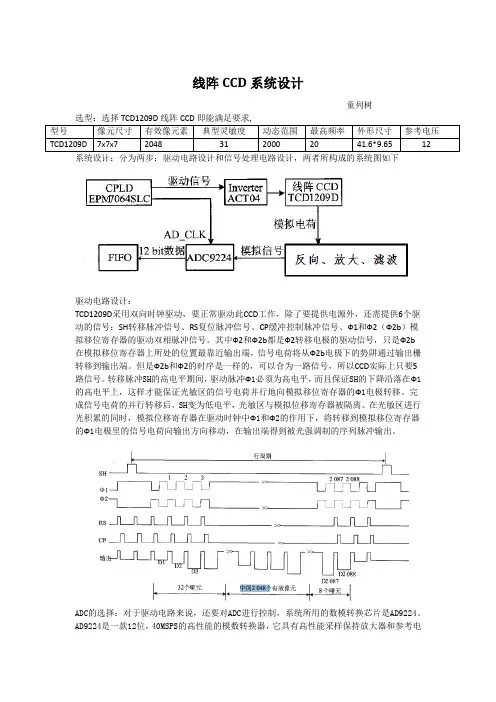
线阵CCD系统设计童列树驱动电路设计:TCD1209D采用双向时钟驱动,要正常驱动此CCD工作,除了要提供电源外,还需提供6个驱动的信号:SH转移脉冲信号、RS复位脉冲信号、CP缓冲控制脉冲信号、Ф1和Ф2(Ф2b)模拟移位寄存器的驱动双相脉冲信号。
其中Ф2和Ф2b都是Ф2转移电极的驱动信号,只是Ф2b在模拟移位寄存器上所处的位置最靠近输出端,信号电荷将从Ф2b电极下的势阱通过输出栅转移到输出端。
但是Ф2b和Ф2的时序是一样的,可以合为一路信号,所以CCD实际上只要5路信号。
转移脉冲SH的高电平期间,驱动脉冲Ф1必须为高电平,而且保证SH的下降沿落在Ф1的高电平上,这样才能保证光敏区的信号电荷并行地向模拟移位寄存器的Ф1电极转移。
完成信号电荷的并行转移后,SH变为低电平,光敏区与模拟位移寄存器被隔离。
在光敏区进行光积累的同时,模拟位移寄存器在驱动时钟中Ф1和Ф2的作用下,将转移到模拟移位寄存器的Ф1电极里的信号电荷向输出方向移动,在输出端得到被光强调制的序列脉冲输出。
ADC的选择:对于驱动电路来说,还要对ADC进行控制,系统所用的数模转换芯片是AD9224。
AD9224是一款12位,40MSPS的高性能的模数转换器,它具有高性能采样保持放大器和参考电压参考。
因为AD9224使用的时候受ADC 时钟的控制,图3所示是其工作的采样时序图。
AD9224 概述:AD9224是一款单芯片、12位、40 MSPS 模数转换器(ADC ),采用单电源供电,内置一个片内高性能采样保持放大器和基准电压源。
AD9224采用多级差分流水线架构,内置输出纠错逻辑,在40 MSPS 数据速率时可提供12位精度,并保证在整个工作温度范围内无失码。
AD9224 特性∙ 低功耗:415 mW ∙ +5 V 单电源 ∙ 保证无失码∙ 微分非线性(DNL )误差:±0.33 LSB ∙ 片内采样保持放大器和基准电压源 ∙ 信噪比(SNR ):68.3 dB∙无杂散动态范围(SFDR ):81 dB ∙ 超量程指示∙ 数据输出格式:标准二进制 ∙ 28引脚SSOP 封装 ∙与3 V 逻辑兼容AD9224 参数AD9224 基本参数分辨率(Bits) 12吞吐率 40 MSPS AD9224 其他特性 工作电压(V) 4.75-5.25 输入通道数 1AD9224 封装与引脚SSOP28信号的调理:在带有模拟电路的设计中,信号的调理成为不可缺少部分。
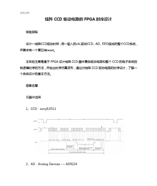
线阵CCD驱动电路的FPGA时序设计实验目标设计一线阵CCD驱动时钟,用一输入的clk,驱动CCD、AD、FIFO组成的整个CCD系统,并要求有一个复位端reset。
本实验主要是基于FPGA设计线阵CCD器件复杂驱动电路和整个CCD的电子系统控制逻辑时序的方法,并给出时序仿真波形,通过对线阵CCD驱动电路的时序设计,了解一个系统设计的基本方法。
总体方案元器件选择1、CCD:sonyILX5112、AD:Analog Devices --- AD92243、FIFO:Integrated Device Technology --- IDT7204方案:FPGA产生CCD线阵、AD、FIFO所需要的驱动时钟,从而实现ccd线阵信号的采集到信号调理,再经由AD进行模数转换后经FIFO 实现信号输出到读接口的过程。
我们需要用一个输入的clk,产生CCD、AD、FIFO所需要的clk,用以驱动它们。
CCD 需要两个时钟:rog和clk,AD和FIFO分别需要一个clk。
实验程序:library ieee;use ieee.std_logic_1164.all;use ieee.std_logic_unsigned.all;entity ccd isport(clk,reset:in std_logic;rog,ccd1,ad1,fifo1:out std_logic);end ccd;architecture ccd_1 of ccd issignal count:integer range 0 to 2130;signal rog2:std_logic;signal ccd2:std_logic;signal ad2:std_logic; signal fifo2:std_logic; beginrog<=rog2;ccd1<=ccd2 or clk; ad1<=ad2 or clk; fifo1<=fifo2 or clk; process(reset,clk) beginif reset='0' thenrog2<='1';ccd2<='1';ad2<='1';count<=0;elsif clk'event and clk='1' then count<=count+1;case count iswhen 0 to 6=>rog2<='1';ccd2<='1';ad2<='1';fifo2<='1';when 7 to 16=>rog2<='0';ccd2<='1';fifo2<='1'; when 17 to 22=> rog2<='1';ccd2<='1';ad2<='1';fifo2<='1'; when 23 to 55=> rog2<='1';ccd2<='0';ad2<='1';fifo2<='1'; when 56 to 58=>ccd2<='0';ad2<='0';fifo2<='1';when 59 to 2106=> rog2<='1';ccd2<='0';ad2<='0';fifo2<='0';when 2107 to 2109=> rog2<='1';ccd2<='0';ad2<='0';when 2110 to 2130=> rog2<='1';ccd2<='0';ad2<='1';fifo2<='1';end case;if count>=2130 then count<=0;end if;end if;end process;end ccd_1;仿真结果:全图:实验报告;通过本次实验加深了对CCD的了解,掌握了VHDL的使用方法,加深了解时序电路的设计法。
基于FPGA的面阵CCD成像系统设计作者:唐艳秋张星祥李新娥任建岳来源:《现代电子技术》2013年第02期摘要:采用SONY 行间转移型面阵CCD ICX415AL 作为图像传感器,设计了一款新型CCD成像系统。
以Altera公司的FPGA芯片EP1C12F256作为时序发生器产生CCD驱动信号。
采用相关双采样技术滤除了视频信号中的相关噪声,提高信噪比。
在Quartus Ⅱ 9.1开发环境下采用VHDL编程,并利用Modelsim SE 6.5仿真软件进行仿真测试。
实验结果表明,所设计的时序满足ICX415AL的时序要求,在29.5 MHz的时钟驱动下,每秒输出50帧图片,能满足高速跟踪要求。
关键词:行间转移型面阵CCD;驱动时序;相关双采样; FPGA中图分类号:TN386.5⁃34 文献标识码:A 文章编号:1004⁃373X(2013)02⁃0123⁃030 引言CCD(Charge Coupled Device)是20世纪70年代初发展起来的新型半导体集成光电器件,它可以把通过光学镜头投影到其上的景物可见光信号转换成比例的电荷包,并在适当的时钟脉冲的驱动下进行定向转移,从而输出成为电压视频图像。
CCD具有集成度高、功耗小、体积小、工作电压低、灵敏度高等优点[1⁃2],目前已广泛应用与空间遥感、对地观测等领域。
按结构分类,CCD可分为线阵CCD和面阵CCD,而面阵CCD按排列方式又可分为全帧转移(Full Frame)CCD、帧转移(Frame Transfer)CCD以及行间转移(Interline Transfer)CCD。
三种类型的CCD各有优缺点,其中行间转移CCD不需要机械快门,速度最快,最适合用于观测快速运动的物体。
本文设计了一种行间转移型面阵CCD的高速驱动电路[3⁃4]。
1 行间转移型面阵CCD的结构和工作模式本设计采用的是SONY公司的ICX415AL型号 CCD芯片,ICX415AL是行间转移型面阵CCD,对角线为8 mm,尺寸为8.3 μm×8.3 μm,总像元素为823(H)×592(V),有效像元为782(H)×582(V)。
基于FPGA的CCD驱动设计作者:武琪敬,李自田,胡炳梁,皮海峰来源:《现代电子技术》2010年第12期摘要:以Atmel公司的面阵CCD-TH7888A图像传感器为例,在研究了CCD结构和驱动时序图的基础上提出基于FPGA的驱动脉冲设计方法和硬件电路实现。
使用VHDL语言对驱动时序发生器进行了硬件描述,并采用Quartus 5.0对设计的驱动时序发生器进行仿真。
试验结果表明,涉及的驱动电路可以满足面阵CCD-TH7888A的各项驱动要求。
关键词:CCD; 信号处理; VHDL; 图像传感器中图分类号文献标识码:A文章编号:1004-373X(2010)12-0157-03Design of CCD Driving Circuit Based on FPGA TechnologyWU Qi----(1. Xi’an Institute of Optics and Precision Mechanics, Chinese Academy of Sciences, Xi’an 710119, China;2. Graduate Student College, Chinese Academy of Sciences, Beijing 100039, China)Abstract:The design and implementation of CCD image sensor digital system is introduced. Taking CCD image sensor TH7888A produced by ATMEL as an example, the FPGA-based hardware driving design is proposed by studying the structure and driver schedule of CCD device. The hardware module and its circuit diagram of the driver are studied, the hardware description is given for the driving schedule generator by VHDL, and then the pulse signal needed by CCD is generated, the designed generator is simulated with Quartus 9.0. The experimental results show that the designed generator can meet the demand of the CCD-TH7888A.Keywords: CCD; signal processing; VHDL; image sensor电荷耦合器件(CCD)作为新兴的固体成像器件即图像传感器,具有体积小,重量轻,分辨力高,噪声低,自扫描,工作速度快,灵敏度高,可靠性好等优点,受到人们的高度重视,广泛应用于图像传感、景物识别、非接触无损检测、文件扫描等领域[1] 。
毕业设计(论文)任务书基于FPGA的LCD驱动显示电路的设计与实现摘要本课题主要任务是设计基于FPGA的LCD驱动电路的设计和实现,兼顾好程序的易用性,以方便之后模块的移植和应用。
控制器部分采用Verilog语言编写,主体程序采用了状态机作为主要控制方式。
最后实现使用FPGA在LCD上显示任意的英文字符和阿拉伯数字,另外要能根据输入数据的变化同步变化LCD上显示的内容。
同时要能将储存模块中的数据正常地显示在LCD上。
该课题的研究将有助于采用FPGA的系列产品的开发,特别是需要用到LCD的产品的开发。
同时可以大大缩短FPGA的开发时间。
另外,由于模块的易用性,也将使得更多的采用FPGA的产品之上出现LCD,增加人机之间的交互性,为行业和我们的生活带来新的变化。
本文中对FPGA,LCD,ModelSim,Xilinx ISE8.2i硬件设计工具等进行了简单的介绍,对其功能进行了简单的描述,并了解了LCD液晶显示器的发展历史,日常应用以及相对比于其他种类显示器的优缺点,并对基于FPGA的LCD液晶显示器驱动电路未来的发展趋势进行了展望。
关键词:FPGA,LCD,状态机,VerilogDesign and Implementation of LCD Drive DisplayCircuit based on FPGAAbstractIn this project, the main object is to design a LCD controller based on FPGA, and at the same time emphasize on the convenience for the later application and migration.The program of the controller is written by Verilog language, and the main body of the program used state machine as the primary control method. displayed picture which was put earlier.In this project, I finally realized the following function. The first one is to display any English and figureon character any position of the display screen. The second one is the display information will instantaneously update as the input data changes.The research of this project will contribute to the developing process of those products which use FPGAs, especially those products also use LCD. And at the same time, it can reduce dramatically on the developing time. In addition, for the convenience of this controller, more and more FPGA based products will come out with LCD screen. This change will enhance the interaction between human and the machine, and bring innovation to the industry and our lives.In this project, FPGA, LCD, ModelSim, Xilinx ISE8.2 I hardware design tools simply introduces its functions were a simple description, and understanding the LCD monitor the development history, and relative everyday applications than in other types of monitor based on FPGA advantages and disadvantages, and the LCD monitor driver circuit future development trends are discussed.Key words:, FPGA, LCD, State Machine, Verilog目录任务书 (I)摘要 ....................................................错误!未定义书签。
基于FPGA的TDICCD8091驱动时序电路设计刘燕;张会生;王靖【摘要】结合时间延时积分图像传感器TDICCD和Altera公司现场可编程门阵列FPGA的器件特点和应用背景,介绍了美国仙童公司的一款高速TDICCD8091的工作特点,在分析其驱动时序信号逻辑关系的基础上,以QuartusⅡ为开发平台采用VHDL硬件描述语言设计并完成时序仿真,经验证该驱动时序下载到硬件电路中能够成功驱动TDICCD8091正常工作。
%In combination with the device characteristics and application backgrounds of time delay and integration charge coupled device(TDICCD)and FPGA,the operating feature of a high-speed TDI sensor TDICCD8091 of the Fairchild Company in USA is introduced. Based on the analysis of the logical relationship of the driving time sequence signals,the timing simula-tion was achieved with VHDL language by taking QuartusⅡ as the development platform. It proved that the driving schedule can successfully drive TDICCD8091 after it was downloaded to the hardware circuit.【期刊名称】《现代电子技术》【年(卷),期】2013(000)017【总页数】3页(P165-167)【关键词】时间延时积分图像传感器;现场可编程门阵列;QuartusⅡ;VHDL【作者】刘燕;张会生;王靖【作者单位】西北工业大学明德学院,陕西西安710124;西北工业大学明德学院,陕西西安 710124;西北工业大学明德学院,陕西西安 710124【正文语种】中文【中图分类】TN29-340 引言时间延时积分电荷耦合器件(Time Delay and Integration Charge Coupled Devices,TDICCD)易于实现实时成像,可与小相对孔径的光学系统配合成像,从而大幅度减少遥感相机的体积和质量,因此广泛应用在航空航天、火控系统和远海探测等领域[1-2]。
第36卷,增刊红外与激光工程2007年9月V01.36Su ppl em e n t妣d粕d Las er Engi nee血g S印.2007基于FPG A大面阵数字C C D相机驱动电路的设计田睿1,刘艳滢2(1.中国科学院研究生院,北京100049;2冲国科学院长春光学精密机械与物理研究所,吉林长春130033)摘要:介绍了大面阵ccD相机的工作时钟产生电路的设计,利用大规模集成电路FPG A实现了该工作时钟驱动电路,采用了V H D L语言对工作时钟驱动电路进行了硬件描述,并利用M odel si I n 软件对所设计的工作时钟驱动电路进行了仿真,最后进行了硬件电路调试,实现了整个cC D相机的控制。
采用SO N Y公司的Icx285A L作为传感器。
关键词:数字C cD相机;FPG A;相关双采样中图分类号:r I P212文献标识码:A文章编号:10ar7.2276(2007)增(探测与制导).0574一04D es i gn of t he dr i V e ci r cui t of t he l ar ge a r r ay C C Dca m er a bas ed on F PG A删Ruil,LⅣY.孤一yin92(1.G r adua tc U n i V e瑙i t y o f C t l i ne se A ca dem y o f Sci锄cc s,Be巧i ng100049,Chi I Ia;2.a啪l gchun I nsm t e of opt ics,F i ne M ec h觚i cs锄d Physi cs,The ch h把∞A ca dem y o f s ciences,ch距gch岫130033,al i n a)A bst r act:I C X285A L C C D s e nsor pr o duc ed by SoN YC o.L t d.ha s bee n us ed i n t hi s C C D c锄em.Thedesi gn of t he ci r cui t w l l i ch can genem t e m e s ched ul e cl ock of t he l a玛e a邺7C C Di s br i e fl y pr e sent ed.FP(;A has be en cho s en a s t he har dw a r e des i gn pl at f o咖t o re al i z e nl e dri ve ci rc ui t,s chedul e ge n e r at or has bee n descr i b ed w i t l l V H D L-T he des i gned gener at or has bee n s uc ce s sf ul l y f ul f i l l ed f unc t i on si m ul撕on w iⅡl M odels i I Il s of t w ar e.Fi nal l y,m e i m pr ove d har dw ar e ci r cui t caI l m e et m e r e q ue s t of t he cont r01of t lle w h01e C C D caI ne r a.K e y w or ds:D珥t al C C D c锄em;FPG A;C伽陷l atcd doubl e s觚l pl er(C D S)0引言数字大面阵ccD相机作为高性能的图像传感器具有动态范围宽、噪声低、灵敏度高等模拟C C D的各种优点,同时兼有大面阵和空间分辨率高、抗干扰能力强等特性,长线传输没有信号损失,有利于远距离信号传输。