Gerber文件各层扩展名与原PCB各层的对应关系
- 格式:docx
- 大小:34.49 KB
- 文档页数:3
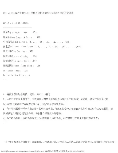
由Protel2004产生的Gerber文件各层扩展名与PCB原来各层对应关系表:Layer : File extension-------------------------顶层Top (copper) Layer : .GTL底层Bottom (copper) Layer : .GBL中间信号层Mid Layer 1, 2, ... , 30 : .G1, .G2, ... , .G30内电层Internal Plane Layer 1, 2, ... , 16 : .GP1, .GP2, ... , .GP16顶丝印层Top Overlay : .GTO底丝印层Bottom Overlay : .GBO顶掩膜层Top Paste Mask : .GTP底掩膜层Bottom Paste Mask : .GBPTop Solder Mask : .GTSBottom Solder Mask : .G……1,编辑元器件时会跑位,变层。
如252118料号2,从99SE或98导出的文件,有些圆弧(如禁止布线层表示要打孔的圆弧等)会隐藏,放大才能看见(如245566料号就曾被投诉漏做安装孔),建议在高版本中查看。
3,和库里元器件一样名称的元器件编辑时会替换,导致孔径变掉。
如251519文件中的CON1和CON3元器件,建议制板时只留自己建的元件库,将软件自带的元件库删除。
4,不支持不规则八角形焊盘与大于6mm的规则八角形焊盘,可在GERBER文件生光栅时留意查看。
……一般PCB基本设计流程如下:前期准备->PCB结构设计->PCB布局->布线->布线优化和丝印->网络和DRC检查和结构检查->制版。
第一:前期准备。
这包括准备元件库和原理图。
……。
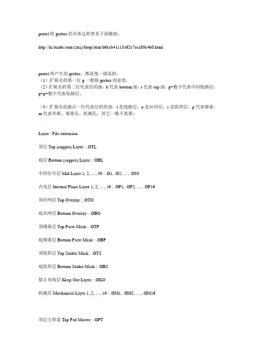
protel转gerber的具体过程参见下面链接:/szxsj/blog/item/b6ecb41113a62c7eca80c4b0.htmlprotel所产生的gerber,都是统一规范的。
(1)扩展名的第一位g一般指gerber的意思。
(2)扩展名的第二位代表层的面,b代表bottom面,t代表top面,g+数字代表中间线路层,g+p+数字代表电源层。
(3)扩展名的最后一位代表层的类别。
l是线路层,o是丝印层,s是阻焊层,p代表锡膏,m代表外框、基准孔、机械孔,其它一般不重要,Layer : File extension顶层Top (copper) Layer : .GTL底层Bottom (copper) Layer : .GBL中间信号层Mid Layer 1, 2, ... , 30 : .G1, .G2, ... , .G30内电层Internal Plane Layer 1, 2, ... , 16 : .GP1, .GP2, ... , .GP16顶丝网层Top Overlay : .GTO底丝网层Bottom Overlay : .GBO顶锡膏层Top Paste Mask : .GTP底锡膏层Bottom Paste Mask : .GBP顶阻焊层Top Solder Mask : .GTS底阻焊层Bottom Solder Mask : .GBS禁止布线层Keep-Out Layer : .GKO机械层Mechanical Layer 1, 2, ... , 16 : .GM1, .GM2, ... , .GM16顶层主焊盘Top Pad Master : .GPT底层主焊盘Bottom Pad Master : .GPB钻孔图层Drill Drawing, Top Layer - Bottom Layer (Through Hole) : .GD1Drill Drawing, other Drill (Layer) Pairs : .GD2, .GD3, ...钻孔引导层Drill Guide, Top Layer - Bottom Layer (Through Hole) : .GG1Drill Guide, other Drill (Layer) Pairs : .GG2, .GG3, ...机械层:定义整个PCB板的外观的,其实我们在说机械层的时候就是指整个PCB板的外形结构。

如何用Protel DXP生成Gerber文件目录:1. 为何要将PCE^件转换为GERBE&件和钻孔数据后交PCB厂制板2. 什么是GERBER件3. Protel DXP 中Design/Board Layers&Color 介绍4. 如何用Protel DXP 生成Gerber文件5. 由Protel2004产生的Gerber文件各层扩展名与PCB原来各层对应关系表6. 两层板和四层板要导出的layers1. 为何要将PC9件转换为GERBER件和钻孔数据后交PCB厂制板大多数工程师都习惯于将PCB^件设计好后直接送PCB厂加工,而国际上比较流行的做法是将PCB^件转换为GERBER:件和钻孔数据后交PCB 厂,为何要“多此一举”呢?因为电子工程师和PCB工程师对PCB的理解不一样,由PCB!厂转换出来的GERBER件可能不是您所要的,如您在设计时将元件的参数都定义在PCB^件中,您又不想让这些参数显示在PC城品上,您未作说明PCB 厂依葫芦画瓢将这些参数都留在了PCB成品上。
这只是一个例子。
若您自己将PCB^件转换成GERBER:件就可避免此类事件发生。
2. 什么是GERBERC件GERBER件是一种国际标准的光绘格式文件,它包含RS-274-D和RS-274-X 两种格式,其中RS-274-D称为基本GERBER式,并要同时附带D码文件才能完整描述一张图形;RS-274-X称为扩展GERBER式,它本身包含有D码信息。
常用的CAca件都能生成此二种格式文件。
Gerber数据是由象片测图仪(Photoplotters )生成的。
象片测图仪由一个精密的伺服系统组成,该系统控制着一个X-Y工作台,上面附着一片高对比度菲林。
光源透过一个快门照在菲林上。
该快门含有一个光圈***并聚焦在菲林上。
控制器把Gerber指令转换为适当的工作台移动,光圈***旋转和快门的开合。
其结果就是我们通常看到的Gerber文件3. Protel DXP 中Design/Board Layers&Color 介绍(1) Signal Layers :信号层ProtelDXP电路板可以有32个信号层,其中Top是顶层,Midi〜30是中间层,Bottom是底层。
solder mask 阻焊剂;焊锡掩膜;绿漆 PCB板各层含义在EDA软件的专门术语中,有很多不是有相同定义的。
以下就字面上可能的意义来解释。
Mechnical:一般多指板型机械加工尺寸标注层。
Keepoutlayer:定义走线、打穿孔(via或摆零件的区域。
这几个限制可以独立分开定义。
Topoverlay:顶丝印层。
Bottomoverlay:底丝印层。
Toppaste:顶层需要露出铜皮上锡膏的部分。
Bottompaste:底层需要露出铜皮上锡膏的部分。
Topsolder:应指顶层阻焊层,避免在制造过程中或将来维修时可能不小心的短路 Bottomsolder:应指底层阻焊层。
Drillguide:可能是不同孔径大小,对应的符号,个数的一个表。
Drilldrawing:指孔位图,各个不同的孔径会有一个对应的符号。
Multilayer:应该没有单独这一层,能指多层板,针对单面板和双面板而言。
Gerber文件各层对照由Protel2004产生的Gerber文件各层扩展名与PCB原来各层对应关系表: Layer : File extension ------------------------- 顶层Top (copper Layer : .GTL 底层Bottom (copper Layer : .GBL 中间信号层Mid Layer 1, 2, ... , 30 : .G1, .G2, ... , .G30 内电层Internal Plane Layer 1, 2, ... , 16 : .GP1, .GP2, ... , .GP16 顶丝印层Top Overlay : .GTO 底丝印层Bottom Overlay : .GBO 顶掩膜层Top Paste Mask : .GTP 底掩膜层Bottom Paste Mask : .GBP Top Solder Mask : .GTS Bottom Solder Mask : .GBS Keep-Out Layer : .GKO Mechanical Layer 1, 2, ... , 16 : .GM1, .GM2, ... , .GM16 Top Pad Master : .GPT Bottom Pad Master : .GPB Drill Drawing, Top Layer - Bottom Layer (Through Hole : .GD1 Drill Drawing, other Drill (Layer Pairs : .GD2, .GD3, ... Drill Guide, Top Layer - Bottom Layer (Through Hole : .GG1 Drill Guide, other Drill (Layer Pairs : .GG2, .GG3, ... 层PCB板就是在多个板层完成后再采取压制工艺将其压制成一块电路板,而且为了减少成本和过孔干扰,多层PCB板往往并不比双层板和单层板厚多少,这就使得组成多层PCB板的板层相对于普通的双层板和单层板往往厚度更小,机械强度更低,导致对加工的要求更高。
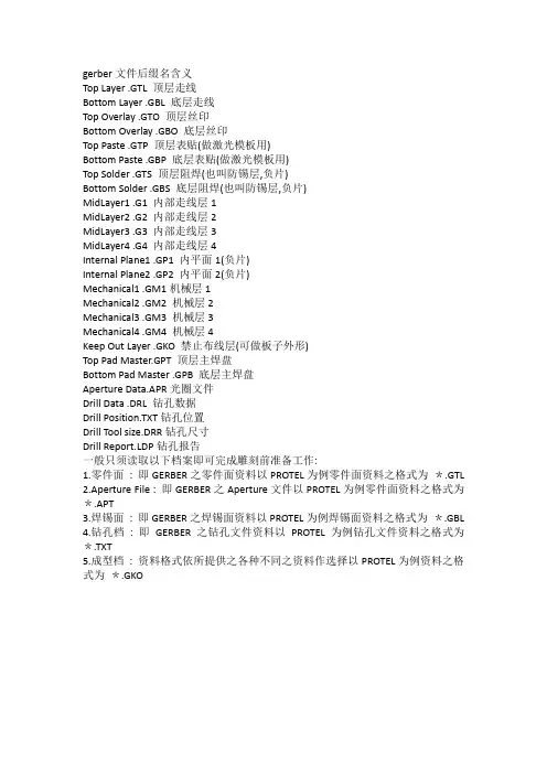
gerber文件后缀名含义Top Layer .GTL 顶层走线Bottom Layer .GBL 底层走线Top Overlay .GTO 顶层丝印Bottom Overlay .GBO 底层丝印Top Paste .GTP 顶层表贴(做激光模板用)Bottom Paste .GBP 底层表贴(做激光模板用)Top Solder .GTS 顶层阻焊(也叫防锡层,负片)Bottom Solder .GBS 底层阻焊(也叫防锡层,负片)MidLayer1 .G1 内部走线层1MidLayer2 .G2 内部走线层2MidLayer3 .G3 内部走线层3MidLayer4 .G4 内部走线层4Internal Plane1 .GP1 内平面1(负片)Internal Plane2 .GP2 内平面2(负片)Mechanical1 .GM1机械层1Mechanical2 .GM2 机械层2Mechanical3 .GM3 机械层3Mechanical4 .GM4 机械层4Keep Out Layer .GKO 禁止布线层(可做板子外形)Top Pad Master.GPT 顶层主焊盘Bottom Pad Master .GPB 底层主焊盘Aperture Data.APR光圈文件Drill Data .DRL 钻孔数据Drill Position.TXT钻孔位置Drill Tool size.DRR钻孔尺寸Drill Report.LDP钻孔报告一般只须读取以下档案即可完成雕刻前准备工作:1.零件面: 即GERBER之零件面资料以PROTEL为例零件面资料之格式为*.GTL2.Aperture File : 即GERBER之Aperture文件以PROTEL为例零件面资料之格式为*.APT3.焊锡面: 即GERBER之焊锡面资料以PROTEL为例焊锡面资料之格式为*.GBL4.钻孔档: 即GERBER之钻孔文件资料以PROTEL为例钻孔文件资料之格式为*.TXT5.成型档: 资料格式依所提供之各种不同之资料作选择以PROTEL为例资料之格式为*.GKO。

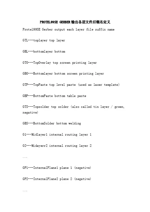
PROTEL99SE GERBER输出各层文件后缀名定义Protel99SE Gerber output each layer file suffix nameGTL---toplayer top layerGBL---bottomlayer bottomGTO---TopOverlay top screen printing layerGBO---Bottomlayer bottom screen printing layerGTP---TopPaste top level paste (used as laser template)GBP---BottomPaste bottom table pasteGTS---Topsolder top solder (also called tin layer / green, negative)GBS---BottomSolder bottom weldingG1---Midlayer1 internal routing layer 1G2---Midayerr2 internal routing layer 2...GP1---InternalPlane1 plane 1 (negative)GP2---InternalPlane2 plane 2 (negative)...GM1---Mechanical1 mechanical layer 1GM2---Mechanical2 mechanical layer 2...GKO---KeepOuter inhibit wiring layerGG1---DrillGuide drilling boot layerGD1---DrillDrawing drill layerGPT---Top pad Master top master padGPB---Bottom pad Master bottom master padGerber file introduction:The standard Gerber file format can be divided into two types, RS-274 and RS-274X, which differ in that:RS-274, Gerber, file, and aperture are separate files.The aperture in RS-274X format is integrated in Gerber file, so there is no need for aperture files (ie, containing D code).Data format: integer bit + decimal digitCommonly used: 3:3 (metric, integer 3, decimal 3)2:4 (Imperial, integer 2, decimal 4)2:3 (Imperial, integer 2, decimal 3)3:3 (Imperial, integer 3, decimal 3)Leading zero, post zero and no zero:Example: 025690 leading zeros change to: 25690 (Leading) After 025690, zero is changed to: 02569 (Trailing)025690 does not lead to zero: 025690 (None)Company:METRIC (mm)ENGLISH (inch, or, mil)Unit conversion:1 inch = 1000 mil = 2.54 cm = 25.4 mm1 mm = 0.03937 inch = 39.37 milData features in GERBER format:Data code: ASCLL, EBCDIC, EIA, ISO code, commonly used: ASC, II code.Data units: Imperial, metric, and common: english.Coordinate forms: relative coordinates, absolute coordinates, commonly used: absolute coordinates.Data form: the former zero, the fixed length, the after zero, commonly used: fixed length.Introduction to polarity of GERBER FILE:Positive (POSITIVE): the GERBER description is the wiring layer, and the graphics depicted are mainly copper parts. Or "GERBER" describes the anti welding layer, and the description of the figure is mainly the anti welding part (that is, the cover ink part).Negative (NEGTIVE): GERBER description is a circuit layer, and the description of graphics is mainly copper parts. Or "GERBER" describes the anti welding layer, and the description of the figure is mainly non welding part (i.e., no ink part).Composite chip (COMPOSTIVE): the layers described by GERBER are synthesized from different polar layers.Usually, the excavation layer and the positive layer are superimposed.The polarity of excavation is C, mainly from line protection or additional process information.GERBER data is a file format that can be generated by all PCBCAD systems that can be processed by all optical plotters. The GERBER format is a subset of the EIA standard RS-274D. The extended GERBER format is a superset of EIA standard RS-274D format, also called RS-274X. RS-274X enhances handling of polygon fill, plus and minus combinations, custom D codes, and other functions. It also defines the rules for embedding an aperture table in the GERBER data file.The GERBER format file consists of a series of data blocks (parameters and code). Each block is separated by a block ending (EOB) symbol. The EOB character is usually an asterisk (*). According to the order in the file, the data blocks fall into the following two categories:1 RS-274X parameterDivided into the following groups in sequence:Prompt parameterAS coordinate selectionFS format descriptionMI mirror imageMO unitOF offsetSF scale factorImage parameterIJ image alignmentIN image nameIO image offsetIP image positive and negativeIR image rotationPF drawing film nameAperture parameterAD aperture descriptionAM aperture customLayer parameterKO excavationLN layer namePositive and negative of LP layer SR mobile and replicationmiscIF embedded file2 standard RS-274D codeIncluding a character function code, such as D code, G code, M code, and coordinate data. The coordinate data in X, Y format describes the linear position, and the I and J format describes the arc position.N Code: sequential code, named block order. (0-99999)D Code: drawing code, select, control the iris, specify the line type.G Code: general purpose code, used for coordinate positioning.M Code: Specifies the end of the file, etc..Example:*G04 THIS IS DEMO annotation%FSLAX23Y23*% omit leading zeros, absolute coordinates X2.3, Y2.3%MOIN*% set inch units%OFA0B0*% no offset%SFA1.0B1.0*% output ratio X axis 1, Y axis 1%ADD10C, 0.010*% defines D10 code as circle, diameter 10MILs The%LNBOXES*% layer is called BOXESG54D10* below is RS0274D dataX0Y0D02*X5000Y0D01*X5000Y5000D01*X0Y5000D01*X0Y0D01*X6000Y0*X11000Y0D01*X6000Y0D01*D02*M02* data overTwo RS-274X parameterFormat:%[]*%Parameter code, double character code (AD, AM, FS, etc.)The modifier completes the parameter code to define the qualifier requiredAD Aperture Definition aperture descriptionData block format:%ADD, [X]*%N1 D code number (10-9999)C (circle) outside diameter, X direction aperture, Y direction apertureThe R (oblong) X extends from size Y to size X to aperture Y to apertureO (ellipse) X from size Y to size X to aperture Y to apertureP (positive, multilateral) outer diameter, rotation angle, X direction aperture, Y apertureAM Aperture Macro custom irisA data block format:%AM*, []*.[[>*,,... *%Defines a name for the current custom apertureGame game1 (circle) Exp, diameter center X, center Y2/20 (line) Exp, line width starting point, X starting point, Y end point, X end point, Y angle21 (oblong) Exp, wide, high, center, X, center, Y angle22 (rectangular) Exp, wide height, left lower X, lower left Yangle4 (polygon) Exp points, starting point X, starting point Y, X1, Y1... angle5 (regular polygon) Exp, top count center, X center, Y diameter6 (Moire) X0 Y0, outer diameter, ring width, ring spacing, rings tens of width, ten long angle7 (heat dissipation) X0, Y0 outside diameter, inner diameter, mouth size angle3 end customAS, Axis, Select axis selectionData block format:%ASA[X|Y]B[X|Y]*%A B output device coordinate axisX Y data file coordinate axisFS Format StatementData block format:%FS[L|T][A|I][Nn][Gn]XnnYnn[Dn][Mn]*%L T L omit leading zero T, omit tail zeroA, I, A, absolute coordinates, I, relative coordinatesIn most EDA software, when designing the PCB, a Solder Mask is defined, which is called the solder layer in production, and the Solder Mask region is not defined on the pad. That is, where the solder and solder resist are produced, if the area is defined too large, the line or other conductive object near the pad will be exposed to the solder resist. Thus, in the process of processing, the bond plate and its vicinity metal wire are easy to form "bridging", causing short circuit phenomenon. Thus, the "Solder Bridges" phenomenon in production is usually caused by the improper definition of the mask data in the design stage and the CAD system is not found in time. Therefore, it is necessary to detect and repair "Solder Bridges" phenomenon quickly before processing.CAM350 not only can quickly find "Solder Bridge", but also can be repaired. Before processing to realize this function as long as the use of Analysis Find Solder Bridges to open the menu - > "Solder Bridging" dialog box.Tick in the "Top Check/Bottom Check" in front of a small box can choose only to detect surface or bottom detection or at the same time. In the following "Mask, Layer, Check, Against", select the correct layer, note that Soldermask_top corresponds to the Top layer; Soldermask_bottom corresponds to the Bottom layer. In Bridge Distance, enter the minimum tolerance bridge spacing. In the following "Search Area", select "Process Entire Layer" to indicate that the system will detect all layers currently open. If you choose "Window Area to Process", you would like to select a window first, and the system will detect the area of the window. After OK, the system will continue to be tested for some time. If an error is detected, a dialog boxis popped up. OK, the screen will jump to another edit window, and an information display / edit bar appears on the upper right.Here you can see all of the error specific locations, you can click on "All" to show all the errors, or you can select a error in the drop-down box, so you can query the specific location of the error.6.Check DrillThis function item is used to examine various problems in the drilling. For example, the distance between the hole and the hole is reasonable, whether or not there are two holes of the same size or different size in the same position.Analysis Check Drill Alalysis - > Drills, pop-up dialog box."Overlapped Drill Hits" can check whether there are two overlapping vias at the same location. "Coincident Drill Hits (Different Sizes)" can test whether there are two or more vias of the same size in the same location, but these vias are produced by different Tools. "Redundant Drill Hits (Same Size") can check whether or not there are two or more vias of the same size at the same location, but these vias are generated by the same Tool. "Drill, Hole, to, Drill, Hole, Clearance" can test whether the spacing between the holes meets certain rules. Next, select the layer you want to test in the Layers to Analyze.More than 7. of the DFM test the function can produce a report in the Info Report menu - > display test results. Such as Sliver,Report, Solder, Mask, Errors, Report, Silkscreen, Errors, Report, etc., and can be saved as a *.rpt file.If you have run the test function, just want to look at their specific location can be achieved by using Info - Find menu. You can also click directly in the dialog box of a menu item under Analysis.3. Copper Slivers"Copper Slivers" refers to those thin and narrow areas of copper that may easily fall off during production. This feature not only detects the narrow areas of copper deposits, but also the repair / trim function. Before you perform this operation, first open the relevant layers that you need to detect. Analysis - > Copper Slivers "Copper Slivers Detection" will pop up a dialog box.The first input can tolerate the minimum number of copper in the "Find Slivers Less than". In "Processing Control", you can choose "Fix Silvers" to repair the fine copper. Select "Remove Old Slivers" to eliminate the detection results that have been generated, such as "Mask Silvers"". In the following "Search Area", select "Process Entire Layer" to indicate that the system will detect all layers currently open. If you choose "Window Area to Process", you would like to select a window first, and the system will detect the area of the window. OK, detection system will continue to end time, finally pops up a message, if no error will show "Found no new Slivers". If you find errors will pop up an error message box, determine the screen will jump to another edit window. You can see all theexact locations here,You can click on "All" to display all the errors, or you can select a error in the drop down box so that you can query the exact location of the error.4.Mask Slivers"Mask Slivers" refers to those thin and narrow areas which are easily removed in the production process (commonly known as "green" solder barrier). Once the solder is removed, the solder is easily slid into the solder, causing undesirable results. This function can be detected and repaired before production, so as not to cause unnecessary consequences. Analysis, Mask Silvers, Mask Sliver Detection, a pop-up dialog box.The first input can tolerate the minimum number of copper in the "Find Slivers less than". In "Processing Control", you can choose "Fix Slivers" to repair the fine copper. Select "Remove Old Slivers" to cancel the previously detected results, such as "Mask Slivers"". In the following "Search Area", select "Process Entire Layre" to indicate that the system will detect all layers currently open. If you choose "Window Area to Process", you would like to select a window first, and the system will detect all layers currently open. After OK, the system will continue to be tested for a while and finally pop up a tooltip message. If there is no error, "Found no new Slivers" will be displayed". If an error is detected, a false dialog box is popped up. OK, the screen will jump to another edit window, and an information display / edit bar appears on the upper right. Here you can see all of the error specificlocations, you can click on "All" to show all the errors, or you can choose a error in the drop-down box, so you can query the specific location of the error.1., Silk, to, Solder, SpacingThis is the software to automatically test the screen printing layer and the spacing of the solder resist. Analysis Silk to Solder Spacing, "Check Silkscreen" dialog box will pop up.First, select the two layer you want to check, that is, Sildcreen_top/Soldermask_top, select both andSildcreen_bottom/Soldermask_bottom at the same time. Then enter the most tolerable spacing in the Clearance. The best tick in the "Remove Old Silkscreen Errors", to avoid confusion. After OK, the system performs the lookup, and at the bottom of the screen shows the "Silk to Sold Check" on the left: the percentage shown on the right shows a message box for error after execution. After "OK", the screen jumps to these two levels of information, and a display / edit bar is added to the top right of the screen. Here you can see all of the error specific locations, you can click on "All" to show all the errors, or you can choose a error in the drop-down box, so you can query the specific location of the error.2., Solder, Mask, to, Trace, SpacingIn general EDA software, defined as Solder Mask place, in fact, when the board is painted solder place. Where there is no Solder Mask, the solder is stopped when the board is made.In the process of welding solder to avoid disorderly flow caused between "pad lead bridge" short circuit main purpose of solder resist, ensure the quality of the installation, to provide electrical environment for a long time and anti chemical protection, forming printed circuit board coat".This command is when an implementation software automatically checks the line and Sold (solder) pitch function.Analysis Solder Mask to Trace - > Spacing, "Check Solder Mask" will pop up a dialog box.In this dialog, select the Electrical Layer and Solder Mask Layer two layers to check respectively. Select theTop/Soldermask_top layer at the same time, or check the Bottom/Soldermask_Bottom layer at the same time. Then enter the minimum tolerable spacing in the Clearance. The best tick in the "Remove Old Solder Mask Errors", to avoid confusion. After OK, the system performs the lookup. At this time, the bottom of the screen shows the "Solder to Trace Check": the percentage displayed on the right. After the execution, if an error is detected, an error message box will pop up.Similarly, the screen will jump to the two level of information after the confirmation, and a display / edit bar will be added to the top right of the screen. Here you can see all of the error specific locations, you can click on "ALL" to show all the errors, or you can select a error in the drop-down box, so you can query the specific location of the error.。

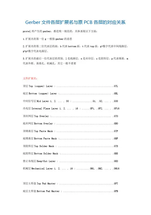
Gerber文件各层扩展名与原PCB各层的对应关系protel所产生的gerber,都是统一规范的,具体表现以下方面:1.扩展名的第一位g一般指gerber的意思2.扩展名的第二位代表层的面,b代表bottom面,t代表top面,g+数字代表中间线路层,g+p+数字代表电源层。
3.扩展名的最后一位代表层的类别。
l是线路层,o是丝印层,s是阻焊层,p代表锡膏,m 代表外框、基准孔、机械孔,其它一般不重要文件扩展名:顶层Top (copper) Layer : ...........................................GTL底层Bottom (copper) Layer :....................................... .GBL中间信号层Mid Layer 1, 2, ... , 30 : ...............G1, .G2, ... . .G30内电层Internal Plane Layer 1, 2, ... , 16 : ......GP1, .GP2, ... . .GP16顶丝网层Top Overlay :............................................. .GTO底丝网层Bottom Overlay : ...........................................GBO顶锡膏层Top Paste Mask : ...........................................GTP底锡膏层Bottom Paste Mask :....................................... .GBP顶阻焊层Top Solder Mask : ..........................................GTS底阻焊层Bottom Solder Mask :...................................... .GBS禁止布线层Keep-Out Layer : .........................................GKO机械层Mechanical Layer 1, 2, ... , 16 : ..........GM1, .GM2, ... , .GM16顶层主焊盘Top Pad Master : .........................................GPT底层主焊盘Bottom Pad Master : ......................................GPB钻孔图层Drill Drawing, Top Layer - Bottom Layer (Through Hole) : ...GD1Drill Drawing, other Drill (Layer) Pairs : ...................GD2, .GD3钻孔引导层Drill Guide, Top Layer - Bottom Layer (Through Hole) : ...GG1Drill Guide, other Drill (Layer) Pairs : .............GG2, .........GG3机械层:定义整个PCB板的外观的,其实我们在说机械层的时候就是指整个PCB板的外形结构.禁止布线层:定义我们在布电气特性的铜一时的边界,也就是说我们先定义了禁止布线层后,我们在以后的布过程中,所布的具有电气特性的线是不可能超出禁止布线层的边界.Top overlay和bottom overlay:定义顶层和底的丝印字符,就是一般我们在PCB板上看到的元件编号和一些字符。

G e r b e r文件各层扩展名与原P C B各层的对应关系YKK standardization office【 YKK5AB- YKK08- YKK2C- YKK18】Gerber文件各层扩展名与原PCB各层的对应关系protel所产生的gerber,都是统一规范的,具体表现以下方面:1.扩展名的第一位g一般指gerber的意思2.扩展名的第二位代表层的面,b代表bottom面,t代表top面,g+数字代表中间线路层,g+p+数字代表电源层。
3.扩展名的最后一位代表层的类别。
l是线路层,o是丝印层,s是阻焊层,p代表锡膏,m 代表外框、基准孔、机械孔,其它一般不重要文件扩展名:顶层Top (copper) Layer : ...........................................GTL底层Bottom (copper) Layer :....................................... .GBL中间信号层Mid Layer 1, 2, ... , 30 : ...............G1, .G2, ... . .G30内电层Internal Plane Layer 1, 2, ... , 16 : ......GP1, .GP2, ... . .GP16顶丝网层Top Overlay :............................................. .GTO底丝网层Bottom Overlay : ...........................................GBO顶锡膏层Top Paste Mask : ...........................................GTP底锡膏层Bottom Paste Mask :....................................... .GBP顶阻焊层Top Solder Mask : ..........................................GTS底阻焊层Bottom Solder Mask :...................................... .GBS禁止布线层Keep-Out Layer : .........................................GKO机械层Mechanical Layer 1, 2, ... , 16 : ..........GM1, .GM2, ... , .GM16顶层主焊盘Top Pad Master : .........................................GPT底层主焊盘Bottom Pad Master : ......................................GPB钻孔图层Drill Drawing, Top Layer - Bottom Layer (Through Hole) : ...GD1Drill Drawing, other Drill (Layer) Pairs : ...................GD2, .GD3钻孔引导层Drill Guide, Top Layer - Bottom Layer (Through Hole) : ...GG1Drill Guide, other Drill (Layer) Pairs : .............GG2, .........GG3机械层:定义整个PCB板的外观的,其实我们在说机械层的时候就是指整个PCB板的外形结构.禁止布线层:定义我们在布电气特性的铜一时的边界,也就是说我们先定义了禁止布线层后,我们在以后的布过程中,所布的具有电气特性的线是不可能超出禁止布线层的边界.Top overlay和bottom overlay:定义顶层和底的丝印字符,就是一般我们在PCB板上看到的元件编号和一些字符。
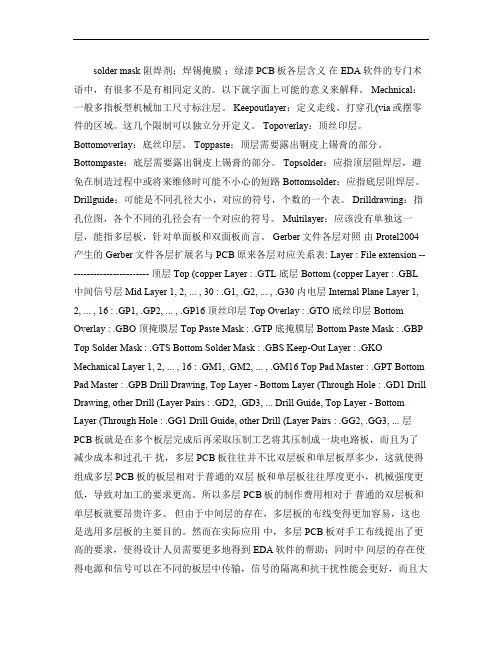
Gerber文件的应用什么是gerber文件GERBER文件是一种国际标准的光绘格式文件,它包含RS-274-D和RS-274-X 两种格式,其中RS-274-D称为基本GERBER格式,并要同时附带D码文件才能完整描述一张图形;RS-274-X称为扩展GERBER格式,它本身包含有D码信息。
常用的CAD软件都能生成此二种格式文件。
Gerber数据是由象片测图仪(Photoplotters)生成的。
象片测图仪由一个精密的伺服系统组成,该系统控制着一个X-Y工作台,上面附着一片高对比度菲林。
光源透过一个快门照在菲林上。
该快门含有一个光圈并聚焦在菲林上。
控制器把Gerber指令转换为适当的工作台移动,光圈旋转和快门的开合。
其结果就是我们通常看到的Gerber文件。
Protel中Design/Board Layers&Color(1)Signal Layers:信号层ProtelDXP电路板可以有32个信号层,其中Top是顶层,Mid1~30是中间层,Bottom是底层。
习惯上Top层又称为元件层,Botton层又称为焊接层。
信号层用于放置连接数字或模拟信号的铜膜走线。
(2)Masks:掩膜Top/Bottom Solder:阻焊层。
阻焊层有2层,用于阻焊膜的丝网漏印,助焊膜防止焊锡随意流动,避免造成各种电气对象之间的短路。
Solder表面意思是指阻焊层,就是用它来涂敷绿油等阻焊材料,从而防止不需要焊接的地方沾染焊锡的,这一层会露出所有需要焊接的焊盘,并且开孔会比实际焊盘要大。
这一层资料需要提供给PCB厂。
Top/Bottom Paste:锡膏层。
锡膏层有2层,用于把表面贴装元件(SMD)粘贴到电路板上。
利用钢膜(Paste Mask)将半融化的锡膏倒到电路板上再把SMD元件贴上去,完成SMD元件的焊接。
Paete表面意思是指焊膏层,就是说可以用它来制作印刷锡膏的钢网,这一层只需要露出所有需要贴片焊接的焊盘,并且开孔可能会比实际焊盘小。
PCB各层含义及Gerber对于不同的设计就有不同的输出Gerber文件数,特别是不同板层的设计差别更大。
但是通常来讲有七种板层数据需要输出,这们分别是:(1)Routing(丝印层):如果是两层以上板,将分为上、下或中间走线层(2)Silkscreen(对于不同的设计就有不同的输出Gerber文件数,特别是不同板层的设计差别更大。
但是通常来讲有七种板层数据需要输出,这们分别是:(1)Routing(丝印层):如果是两层以上板,将分为上、下或中间走线层(2)Silkscreen(丝印层):多层板有上、下两层,如果底层没有丝印,则不用出;(3)Plane(电源、地平面层):只是针对多层板而言(以负片输出);(4)Paste Mask(SMD贴片层);主要针对板上的SMD元件。
如果板全部放置的是Dip(通孔)元件,这一层就不用输出Gerber文件了。
在将SMD元件贴板上以前,必须在每一个SMD焊盘上先涂上锡膏,在涂锡用的钢网就一定需要这个Paste Mask文件,菲林胶片才可以加工出来。
Paste Mask层的Gerber输出最重要的一点要清楚,即这个层主要针对SMD元件,同时将这个层与下面即将介绍的Solder Mask作一比较,弄清两者的不同作用,因为从菲林胶片图中看这两个胶片图很相似。
(5)Solder Mask(主焊层);主要用途是保证被选项(比如元件脚焊盘和某些特殊的铜皮等)在板上不被绿油覆盖而直接以铜皮的形式出现在板上,凡是需要焊接与贴的对象都一定要选择,简单地讲,在设计中如果希望某对象以裸铜的形式出现在板上,那么在输出主焊层就可以把它选上。
对于主焊层Gerber,输出选项Pads(焊盘)一定需要选择,但是主焊层的Pads(元件脚焊盘)跟PastMask中不一样,它包括了SMD和Dip两种焊盘,而PastMask却只包含SMD 焊盘。
(6)NC Drill(NC钻孔层);对于有通孔的板设计,NC Drill输出文件必不可少的,没有这个文件就没法给板钻孔。
G e r b e r文件各层扩展名与原P C B各层的对应关系公司内部编号:(GOOD-TMMT-MMUT-UUPTY-UUYY-DTTI-G e r b e r文件各层扩展名与原P C B各层的对应关系protel所产生的gerber,都是统一规范的,具体表现以下方面:1.扩展名的第一位g一般指gerber的意思2.扩展名的第二位代表层的面,b代表bottom面,t代表top面,g+数字代表中间线路层,g+p+数字代表电源层。
3.扩展名的最后一位代表层的类别。
l是线路层,o是丝印层,s是阻焊层,p代表锡膏,m代表外框、基准孔、机械孔,其它一般不重要文件扩展名:顶层Top (copper) Layer : ...........................................GTL底层Bottom (copper) Layer :....................................... .GBL中间信号层Mid Layer 1, 2, ... , 30 : ...............G1, .G2, ... . .G30内电层Internal Plane Layer 1, 2, ... , 16 : ......GP1, .GP2, ... . .GP16顶丝网层Top Overlay :............................................. .GTO底丝网层Bottom Overlay : ...........................................GBO顶锡膏层Top Paste Mask : ...........................................GTP底锡膏层Bottom Paste Mask :....................................... .GBP顶阻焊层Top Solder Mask : ..........................................GTS底阻焊层Bottom Solder Mask :...................................... .GBS禁止布线层Keep-Out Layer : .........................................GKO机械层Mechanical Layer 1, 2, ... , 16 : ..........GM1, .GM2, ... , .GM16顶层主焊盘Top Pad Master : .........................................GPT底层主焊盘Bottom Pad Master : ......................................GPB钻孔图层Drill Drawing, Top Layer - Bottom Layer (Through Hole) : ...GD1Drill Drawing, other Drill (Layer) Pairs : ...................G D2, .GD3钻孔引导层Drill Guide, Top Layer - Bottom Layer (Through Hole) : ...GG1Drill Guide, other Drill (Layer) Pairs : .............GG2, .........GG3机械层:定义整个PCB板的外观的,其实我们在说机械层的时候就是指整个PCB板的外形结构.禁止布线层:定义我们在布电气特性的铜一时的边界,也就是说我们先定义了禁止布线层后,我们在以后的布过程中,所布的具有电气特性的线是不可能超出禁止布线层的边界.Top overlay和bottom overlay:定义顶层和底的丝印字符,就是一般我们在PCB板上看到的元件编号和一些字符。
PCBGERBER文件扩展名所代表的意义在使用PCB GERBER文件时,经常会碰到如下扩展名的文件,像APR, GKO, GM, GTL, GTO, GTP, GTS, GPT, GD等等,有没有高手来说明下这些扩展名的文件分别和焊盘,防焊油,文字丝印等的一一对应关系。
*.GTL:顶层元件面*.GBL:底层焊接面*.GTO:元件面字符*.GTS:元件面阻焊*.GBS:焊接面阻焊*.GBO:焊接面字符*.APT:D码表文件*.G?:机械某层*.A??:各层的D码表*.GM?:中间某层*.GDD:地线层*.GPW:电源层Top Layer .GTL 顶层走线*.GTLBottom Layer .GBL 底层走线*.GBLTop Overlay .GTO 顶层丝印*.GTOBottom Overlay .GBO 底层丝印*.GB0Top Paste .GTP 顶层表贴(做激光模板用) *.GTPBottom Paste .GBP 底层表贴(做激光模板用) *.GBPTop Solder .GTS 顶层阻焊(也叫防锡层,负片) *.GTSBottom Solder .GBS 底层阻焊(也叫防锡层,负片) *.GBSMidLayer1 .G1 内部走线层1MidLayer2 .G2 内部走线层2MidLayer3 .G3 内部走线层3MidLayer4 .G4 内部走线层4Internal Plane1 .GP1 内平面1(负片)Internal Plane2 .GP2 内平面2(负片)Mechanical1 .GM1机械层1Mechanical2 .GM2 机械层2Mechanical3 .GM3 机械层3Mechanical4 .GM4 机械层4Keep Out Layer .GKO 禁止布线层(可做板子外形) *.GK0 Top Pad Master.GPT 顶层主焊盘*.GPTBottom Pad Master .GPB 底层主焊盘*.GPB Aperture Data.APR光圈文件Drill Data .DRL 钻孔数据Drill Position.TXT钻孔位置Drill Tool size.DRR钻孔尺寸Drill Report.LDP钻孔报告。
GERBER后缀解释1.Top Layer .GTL 顶层走线2.Bottom Layer .GBL 底层走线3.Top Overlay .GTO 顶层丝印4.Bottom Overlay .GBO 底层丝印5.Top Paste .GTP 顶层表贴(做激光模板用)6.Bottom Paste .GBP 底层表贴(做激光模板用)7.Top Solder .GTS 顶层阻焊(也叫防锡层,负片)8.Bottom Solder .GBS 底层阻焊(也叫防锡层,负片)9.MidLayer1 .G1 内部走线层110.MidLayer2 .G2 内部走线层211.MidLayer3 .G3 内部走线层312.MidLayer4 .G4 内部走线层413.Internal Plane1 .GP1 内平面1(负片)14.Internal Plane2 .GP2 内平面2(负片)15.Mechanical1 .GM1机械层116.Mechanical2 .GM2 机械层217.Mechanical3 .GM3 机械层318.Mechanical4 .GM4 机械层419.Keep Out Layer .GKO 禁止布线层(可做板子外形)20.Top Pad Master.GPT 顶层主焊盘21.Bottom Pad Master .GPB 底层主焊盘22.Aperture Data.APR光圈文件23.Drill Data .DRL 钻孔数据24.Drill Position.TXT钻孔位置25.Drill Tool size.DRR钻孔尺寸26.Drill Report.LDP钻孔报告(不用送给厂商)。
Gerber文件各层扩展名与原PCB各层的对应关系
protel所产生的gerber,都是统一规范的,具体表现以下方面:
1.扩展名的第一位g一般指gerber的意思
2.扩展名的第二位代表层的面,b代表bottom面,t代表top面,g+数字代表中间线路层,g+p+数字代表电源层。
3.扩展名的最后一位代表层的类别。
l是线路层,o是丝印层,s是阻焊层,p代表锡膏,m 代表外框、基准孔、机械孔,其它一般不重要
文件扩展名:
顶层Top (copper) Layer : ...........................................GTL
底层Bottom (copper) Layer :....................................... .GBL
中间信号层Mid Layer 1, 2, ... , 30 : ...............G1, .G2, ... . .G30
内电层Internal Plane Layer 1, 2, ... , 16 : ......GP1, .GP2, ... . .GP16
顶丝网层Top Overlay :............................................. .GTO
底丝网层Bottom Overlay : ...........................................GBO
顶锡膏层Top Paste Mask : ...........................................GTP
底锡膏层Bottom Paste Mask :....................................... .GBP
顶阻焊层Top Solder Mask : ..........................................GTS
底阻焊层Bottom Solder Mask :...................................... .GBS
禁止布线层Keep-Out Layer : .........................................GKO
机械层Mechanical Layer 1, 2, ... , 16 : ..........GM1, .GM2, ... , .GM16
顶层主焊盘Top Pad Master : .........................................GPT
底层主焊盘Bottom Pad Master : ......................................GPB
钻孔图层Drill Drawing, Top Layer - Bottom Layer (Through Hole) : ...GD1
Drill Drawing, other Drill (Layer) Pairs : ...................GD2, .GD3
钻孔引导层Drill Guide, Top Layer - Bottom Layer (Through Hole) : ...GG1
Drill Guide, other Drill (Layer) Pairs : .............GG2, .........GG3
机械层:定义整个PCB板的外观的,其实我们在说机械层的时候就是指整个PCB板的外形结构.
禁止布线层:定义我们在布电气特性的铜一时的边界,也就是说我们先定义了禁止布线层后,我们在以后的布过程中,所布的具有电气特性的线是不可能超出禁止布线层的边界.
Top overlay和bottom overlay:定义顶层和底的丝印字符,就是一般我们在PCB板上看到的元件编号和一些字符。
Top paste和bottom paste:顶层底焊盘层,它就是指我们可以看到的露在外面的铜铂,比如我们在顶层布线层画了一根导线这根导线我们在PCB上所看到的只是一根线而已,它是被整个绿油盖住的,但是我们在这根线的位置上的top paset层上画一个方形,或一个点。
所打出来的板上这个方形和这个点就没有绿油了,而是铜铂。
Top solder和bottom solder这两个层刚刚和前面两个层相反,可以这样说,这两个层就是要盖绿油的层,multilaye这个层实际上就和机械层差不多了,顾名恩义,这个层就是指PCB板的所有层。
附生成的Gerber?文件:。