SFL659_规格书_final_v1 0
- 格式:pdf
- 大小:290.88 KB
- 文档页数:8


L6599D中⽂资料May 2006 Rev 11/36L6599High-voltage resonant controllerFeatures■50% duty cycle, variable frequency control of resonant half-bridge ■High-accuracy oscillator■Up to 500kHz operating frequency■Two-level OCP: frequency-shift and latched shutdown■Interface with PFC controller ■Latched disable input■Burst-mode operation at light load ■Input for power-ON/OFF sequencing or brownout protection■Non-linear soft-start for monotonic output voltage rise■600V-rail compatible high-side gate driver with integrated bootstrap diode and high dV/dt immunity■-300/800mA high-side and low-side gate drivers with UVLO pull-down ■DIP-16, SO-16N packagesApplications■LCD & PDP TV■Desktop PC, entry-level server ■Telecom SMPS■AC-DC adapter, open frame SMPSOrder codePart number Package Packaging L6599D SO-16N T ube L6599TR SO-16N Tape and reelL6599NDIP-16T ube/doc/128b95b11a37f111f1855bea.htmlContents L6599Contents1Device description . . . . . . . . . . . . . . . . . . . . . . . . . . . . . . . . . . . . . . . . . . 32Pin Settings . . . . . . . . . . . . . . . . . . . . . . . . . . . . . . . . . . . . . . . . . . . . . . . . 42.1Connection . . . . . . . . . . . . . . . . . . . . . . . . . . . . . . . . . . . . . . . . . . . . . . . . . 42.2Functions . . . . . . . . . . . . . . . . . . . . . . . . . . . . . . . . . . . . . . . . . . . . . . . . . . 4 3Typical system block diagram . . . . . . . . . . . . . . . . . . . . . . . . . . . . . . . . . 64Electrical data . . . . . . . . . . . . . . . . . . . . . . . . . . . . . . . . . . . . . . . . . . . . . . 74.1Maximum ratings . . . . . . . . . . . . . . . . . . . . . . . . . . . . . . . . . . . . . . . . . . . . 74.2Thermal data . . . . . . . . . . . . . . . . . . . . . . . . . . . . . . . . . . . . . . . . . . . . . . . 7 5Electrical characteristics . . . . . . . . . . . . . . . . . . . . . . . . . . . . . . . . . . . . . 8 6Typical electrical performance . . . . . . . . . . . . . . . . . . . . . . . . . . . . . . . . 117Application information . . . . . . . . . . . . . . . . . . . . . . . . . . . . . . . . . . . . . 157.1Oscillator . . . . . . . . . . . . . . . . . . . . . . . . . . . . . . . . . . . . . . . . . . . . . . . . . 167.2Operation at no load or very light load . . . . . . . . . . . . . . . . . . . . . . . . . . . 187.3Soft-start . . . . . . . . . . . . . . . . . . . . . . . . . . . . . . . . . . . . . . . . . . . . . . . . . . 217.4Current sense, OCP and OLP . . . . . . . . . . . . . . . . . . . . . . . . . . . . . . . . . 237.5Latched shutdown . . . . . . . . . . . . . . . . . . . . . . . . . . . . . . . . . . . . . . . . . . 277.6Line sensing function . . . . . . . . . . . . . . . . . . . . . . . . . . . . . . . . . . . . . . . . 277.7Bootstrap section . . . . . . . . . . . . . . . . . . . . . . . . . . . . . . . . . . . . . . . . . . . 297.8Application example . . . . . . . . . . . . . . . . . . . . . . . . . . . . . . . . . . . . . . . . . 31 8Package mechanical data . . . . . . . . . . . . . . . . . . . . . . . . . . . . . . . . . . . . 33 9Revision history . . . . . . . . . . . . . . . . . . . . . . . . . . . . . . . . . . . . . . . . . . . 352/36L6599Device description3/361 Device descriptionThe L6599 is a double-ended controller specific for the resonant half-bridge topology. Itprovides 50% complementary duty cycle: the high-side switch and the low-side switch are driven ON 180° out-of-phase for exactly the same time.Output voltage regulation is obtained by modulating the operating frequency. A fixed dead-time inserted between the turn-OFF of one switch and the turn-ON of the other one guarantees soft-switching and enables high-frequency operation.To drive the high-side switch with the bootstrap approach, the IC incorporates a high-voltage floating structure able to withstand more than 600V with a synchronous-driven high-voltage DMOS that replaces the external fast-recovery bootstrap diode.The IC enables the designer to set the operating frequency range of the converter by means of an externally programmable oscillator.At start-up, to prevent uncontrolled inrush current, the switching frequency starts from a programmable maximum value and progressively decays until it reaches the steady-state value determined by the control loop. This frequency shift is non linear to minimize output voltage overshoots; its duration is programmable as well.The IC can be forced to enter a controlled burst-mode operation at light load, so as to keep converter's input consumption to a minimum.IC's functions include a not-latched active-low disable input with current hysteresis useful for power sequencing or for brownout protection, a current sense input for OCP with frequency shift and delayed shutdown with automatic restart.A higher level OCP latches off the IC if the first-level protection is not sufficient to control the primary current. Their combination offers complete protection against overload and short circuits. An additional latched disable input (DIS) allows easy implementation of OTP and/or OVP .An interface with the PFC controller is provided that enables to switch off the pre-regulator during fault conditions, such as OCP shutdown and DIS high, or during burst-mode operation.Pin Settings L65994/362 Pin Settings2.1 Connection2.2 FunctionsTable 1.Pin functionsN.NameFunction1C SSSoft start. This pin connects an external capacitor to GND and a resistor to RFmin (pin 4)that set both the maximum oscillator frequency and the time constant for the frequency shift that occurs as the chip starts up (soft-start). An internal switch discharges this capacitor every time the chip turns OFF (V CC < UVLO, LINE < 1.25V or > 6V , DIS > 1.85V , ISEN > 1.5V , DELAY > 3.5V) to make sure it will be soft-started next, and when the voltage on the current sense pin (ISEN) exceeds 0.8V , as long as it stays above 0.75V .2DELAYDelayed shutdown upon overcurrent. A capacitor and a resistor are connected from this pin to GND to set both the maximum duration of an overcurrent condition before the IC stops switching and the delay after which the IC restarts switching. Every time the voltage on the ISEN pin exceeds 0.8V the capacitor is charged by an internal 150µA current generator and is slowly discharged by the external resistor. If the voltage on the pin reaches 2V , the soft start capacitor is completely discharged so that the switching frequency is pushed to its maximum value and the 150µA is kept always on. As the voltage on the pin exceeds 3.5V the IC stops switching and the internal generator is turned OFF , so that the voltage on the pin will decay because of the external resistor. The IC will be soft-restarted as the voltage drops below 0.3V . In this way, under short circuit conditions, the converter will work intermittently with very low input average power.3CFTiming capacitor. A capacitor connected from this pin to GND is charged and discharged by internal current generators programmed by the external network connected to pin 4 (RFmin) and determines the switching frequency of the converter.L6599Pin Settings5/364RFminMinimum oscillator frequency setting. This pin provides a precise 2V reference and a resistor connected from this pin to GND defines a current that is used to set the minimum oscillator frequency. T o close the feedback loop that regulates the converter output voltage bymodulating the oscillator frequency, the phototransistor of an optocoupler will be connected to this pin through a resistor. The value of this resistor will set the maximum operatingfrequency. An R-C series connected from this pin to GND sets frequency shift at start-up to prevent excessive energy inrush (soft-start).5STBYBurst-mode operation threshold. The pin senses some voltage related to the feedbackcontrol, which is compared to an internal reference (1.25V). If the voltage on the pin is lower than the reference, the IC entersan idle state and its quiescent current is reduced. The chip restarts switching as the voltage exceeds the reference by 50mV . Soft-start is not invoked. This function realizes burst-mode operation when the load falls below a level that can be programmed by properly choosing the resistor connecting the optocoupler to pin RFmin (see block diagram). Tie the pin to RFmin if burst-mode is not used.6ISENCurrent sense input. The pin senses the primary current though a sense resistor or acapacitive divider for lossless sensing. This input is not intended for a cycle-by-cycle control; hence the voltage signal must be filtered to get average current information. As the voltage exceeds a 0.8V threshold (with 50mV hysteresis), the soft-start capacitor connected to pin 1 is internally discharged: the frequency increases hence limiting the power throughput. Under output short circuit, this normally results in a nearly constant peak primary current. This condition is allowed for a maximum time set at pin 2. If the current keeps on building up despite this frequency increase, a second comparator referenced at 1.5V latches the device off and brings its consumption almost to a “before start-up” level. The information is latched and it is necessary to recycle the supply voltage of the IC to enable it to restart: the latch is removed as the voltage on the Vcc pin goes below the UVLO threshold. Tie the pin to GND if the function is not used.7LINELine sensing input. The pin is to be connected to the high-voltage input bus with a resistor divider to perform either AC or DC (in systems with PFC) brownout protection. A voltage below 1.25V shuts down (not latched) the IC, lowers its consumption and discharges the soft-start capacitor. IC’s operation is re-enabled (soft-started) as the voltage exceeds 1.25V . The comparator is provided with current hysteresis: an internal 15µA current generator is ON as long as the voltage applied at the pin is below 1.25V and is OFF if this value is exceeded. Bypass the pin with a capacitor to GND to reduce noise pick-up. The voltage on the pin is top-limited by an internal zener. Activating the zener causes the IC to shut down (not latched). Bias the pin between 1.25 and 6V if the function is not used.8DISLatched device shutdown. Internally the pin connects a comparator that, when the voltage on the pin exceeds 1.85V , shuts the IC down and brings its consumption almost to a “before start-up” level. The information is latched and it is necessary to recycle the supply voltage of the IC to enable it to restart: the latch is removed as the voltage on the V CC pin goes below the UVLO threshold. Tie the pin to GND if the function is not used.9PFC_STOPOpen-drain ON/OFF control of PFC controller. This pin, normally open, is intended forstopping the PFC controller, for protection purpose or during burst-mode operation. It goes low when the IC is shut down by DIS > 1.85V , ISEN > 1.5V , LINE > 6V and STBY < 1.25V .The pin is pulled low also when the voltage on pin DELAY exceeds 2V and goes back open as the voltage falls below 0.3V . During UVLO, it is open. Leave the pin unconnected if not used.10GNDChip ground. Current return for both the low-side gate-drive current and the bias current of the IC. All of the ground connections of the bias components should be tied to a track going to this pin and kept separate from any pulsed current return.Table 1.Pin functionsTypical system block diagram L65996/363 Typical system block diagramTypical system block diagram11LVGLow-side gate-drive output. The driver is capable of 0.3A min. source and 0.8A min. sink peak current to drive the lower MOSFET of the half-bridge leg. The pin is actively pulled to GND during UVLO.12V CC Supply Voltage of both the signal part of the IC and the low-side gate driver. Sometimes a small bypass capacitor (0.1µF typ.) to GND might be useful to get a clean bias voltage for the signal part of the IC.13N.C.High-voltage spacer. The pin is not internally connected to isolate the high-voltage pin and ease compliance with safety regulations (creepage distance) on the PCB.14OUTHigh-side gate-drive floating ground. Current return for the high-side gate-drive current. Layout carefully the connection of this pin to avoid too large spikes below ground.15HVGHigh-side floating gate-drive output. The driver is capable of 0.3A min. source and 0.8A min. sink peak current to drive the upper MOSFET of the half-bridge leg. A resistor internally connected to pin 14 (OUT) ensures that the pin is not floating during UVLO.16VBOOTHigh-side gate-drive floating supply Voltage. The bootstrap capacitor connected between this pin and pin 14 (OUT) is fed by an internal synchronous bootstrap diode driven in-phase with the low-side gate-drive. This patented structure replaces the normally used external diode.Table 1.Pin functionsL6599Electrical data7/364 Electrical data4.1 Maximum ratingsNote:ESD immunity for pins 14, 15 and 16 is guaranteed up to 900V4.2 Thermal dataTable 2.Absolute maximum ratingsSymbol Pin ParameterValue Unit V BOOT 16 Floating supply voltage -1 to 618 V V OUT 14 Floating ground voltage -3 to V BOOT -18V dV OUT /dt 14 Floating ground max. slew rate 50V/nsV CC 12 IC Supply voltage (I CC ≤ 25 mA) Self-limited V V PFC_STOP 9 Maximum voltage (pin open) -0.3 to V CC V I PFC_STOP 9 Maximum sink current (pin low)AV LINEmax 7Maximum pin voltage (Ipin ≤ 1mA) Self-limited VI RFmin4 Maximum source current 2 mA 1 to 6, 8 Analog inputs & outputs-0.3 to 5VTable 3.Thermal dataSymbol DescriptionValue Unit R thJA Max. thermal resistance junction to ambient (DIP16)80°C/W Max. thermal resistance junction to ambient (SO16)120T STG Storage temperature range-55 to 150°C T J Junction operating temperature range-40 to 150°C P TOTRecommended max. power dissipation @T A = 70°C (DIP16) 1 WRecommended max. power dissipation @T A = 50°C (SO16)0.835 ElectricalcharacteristicsT J = 0 to 105°C, V CC = 15V, V BOOT = 15V, C HVG = C LVG = 1nF; C F = 470pF;R RFmin = 12k?; unless otherwise specified.Table 4.Electrical characteristicsSymbol Parameter TestconditionMin Typ Max Unit IC supply voltageV CC Operating range After device turn-on8.85 16 VV CC(ON)Turn-ON threshold Voltage rising10 10.7 11.4 VV CC(OFF)Turn-OFF threshold Voltagefalling 7.45 8.15 8.85 V Hys Hysteresis 2.55 VV Z V CC clamp voltage Iclamp = 10mA 16 17 17.9 V Supply currentI start-up Start-up current Before device turn-ONV CC = V CC(ON) - 0.2V200 250 µAI q Quiescent current Device ON, V STBY = 1V 1.5 2 mAI op Operating current Device ON,V STBY = V RFmin 3.5 5 mAI q Residual consumption V DIS> 1.85V or V DELAY> 3.5V or V LINE < 1.25 Vor V LINE = V clamp300 400 µAHigh-side floating gate-drive supplyI LKBOOT V BOOT pin leakagecurrentV BOOT= 580V 5 µAI LKOUT OUT pin leakage current VOUT= 562V 5 µAr DS(on)Synchronous bootstrapdiode ON-resistanceV LVG= High 150 ?Overcurrent comparatorI ISEN Input bias current V ISEN = 0 to V ISENdis-1 µAt LEB Leading edge blanking After V HVG and V LVGlow-to-high transition250 nsV ISENx Frequency shiftthreshold Voltage rising(1)0.76 0.8 0.84 VHysteresis Voltagefalling 50 mV V ISENdis Latch OFF threshold Voltage rising (1) 1.44 1.5 1.56 V td(H-L)Delay to output 300400 ns8/369/36Symbol Parameter Test condition Min Typ Max UnitLine sensing V th Threshold voltage Voltage rising or falling(1)1.2 1.25 1.3 V I Hyst Current hysteresis V CC > 5V , V LINE = 0.3V 12 15 18 µA V clamp Clamp levelI LINE = 1mA6 8 VDIS functionI DIS Input bias current V DIS = 0 to V th -1 µAV th Disable thresholdVoltage rising (1)1.77 1.85 1.93 VOscillatorDOutput duty cycleBoth HVG and LVG4850 52 %f oscOscillation frequency58.2 60 61.8kHzR RFmin = 2.7 k ?240 250 260Maximumrecommended500kHz T D Dead-time Between HVG and LVG0.20.3 0.4µs V CFp Peak value 3.9 V V CFv Valley value 0.9 VV REF Voltage reference at pin 4(1)1.92 22.08 VK M Current mirroring ratio 1A/A RF MINTiming resistor range1100k ?PFC_STOP functionI leak High level leakage currentV PFC_STOP = V CC ,V DIS = 0V 1 µAV LLow saturation levelI PFC_STOP =1mA,V DIS = 2V0.2 VSoft-start functionI leakOpen-state currentV(Css) = 2V0.5µA R Discharge resistance V ISEN > V ISENx 120Standby functionI DIS Input Bias Current V DIS = 0 to V th -1 µAV thDisable thresholdVoltage falling (1) 1.2 1.25 1.3 VHys HysteresisVoltage rising50mVTable 4.Electrical characteristics10/36Symbol Parameter Test condition Min TypMax UnitDelayed shutdown functionI leak Open-state current V(DELAY) = 0 0.5 µAI CHARGE Charge current V DELAY = 1V , V ISEN = 0.85V 100 150 200 µA Vth 1 Threshold for forcedoperation at max. frequencyVoltage rising (1)1.92 22.08 VVth 2Shutdown threshold Voltage rising (1) 3.3 3.5 3.7 V Vth 3Restart thresholdVoltage falling (1)0.25 0.3 0.35 VLow - side gate driver (voltages referred to GND)V LVGL Output low voltage I sink = 200mA 1.5 VV LVGH Output high voltage I source = 5mA12.8 13.3 V I sourcepk Peak source current -0.3 A I sinkpk Peak sink current 0.8A t f Fall time 30 ns t rRise time 60nsUVLO saturationV CC = 0 to V CC(ON),I sink = 2mA 1.1 VHigh-side gate driver (voltages referred to OUT)V HVGL Output low voltage I sink = 200 mA 1.5 V V HVGH Output high voltage I source = 5 mA12.8 13.3 V I sourcepk Peak source current -0.3 A I sinkpk Peak sink current 0.8A t f Fall time 30 ns t rRise time60 ns HVG-OUT pull-down25k ?1.Values traking each otherTable 4.Electrical characteristics11/366 Typical electrical performanceFigure 3.Device consumption vssupply voltageFigure 4.IC consumption vs junction temperatureV CC clamp voltage vs junction temperatureFigure 6.UVLO thresholds vs junction temperature12/36Figure 7.Oscillator frequency vsjunction temperature Figure 8.Dead-time vsjunction temperatureFigure 9.Oscillator frequency vstiming components Figure 10.Oscillator ramp vs junction temperature13/36Figure 11.Reference voltage vsjunction temperatureFigure 12.Current mirroring ratio vsjunction temperatureFigure 13.OCP delay source current vsjunction temperature Figure 14.OCP delay thresholds vs junction temperatureFigure 15.Standby thresholds vsjunction temperatureFigure 16.Current sense thresholds vsjunction temperatureFigure 17.Line thresholds vsjunction temperatureFigure 18.Line source current vsjunction temperatureFigure /doc/128b95b11a37f111f1855bea.html tched disable threshold vs junction temperature7 ApplicationinformationThe L6599 is an advanced double-ended controller specific for resonant half-bridge topology. In these converters the switches (MOSFETs) of the half-bridge leg are alternately switched on and OFF (180° out-of-phase) for exactly the same time. This is commonly referred to as operation at "50% duty cycle", although the real duty cycle, that is the ratio of the ON-time of either switch to the switching period, is actually less than 50%. The reason is that there is an internally fixed dead-time T D, inserted between the turn-OFF of either MOSFET and the turn-ON of the other one, where both MOSFETs are OFF. This dead- time is essential in order for the converter to work correctly: it will ensure soft-switching and enable high-frequency operation with high efficiency and low EMI emissions.To perform converter's output voltage regulation the device is able to operate in different modes (Figure20), depending on the load conditions:1.Variable frequency at heavy and medium/light load. A relaxation oscillator (see "Oscillator" section for more details) generates a symmetrical triangular waveform,which MOSFETs' switching is locked to. The frequency of this waveform is related to a current that will be modulated by the feedback circuitry. As a result, the tank circuitdriven by the half-bridge will be stimulated at a frequency dictated by the feedback loopto keep the output voltage regulated, thus exploiting its frequency-dependent transfer characteristics.2. Burst-mode control with no or very light load. When the load falls below a value, the converter will enter a controlled intermittent operation, where a series of a fewswitching cycles at a nearly fixed frequency are spaced out by long idle periods whereboth MOSFETs are in OFF-state. A further load decrease will be translated into longeridle periods and then in a reduction of the average switching frequency. When theconverter is completely unloaded, the average switching frequency can go down evento few hundred Hz, thus minimizing magnetizing current losses as well as all frequency-related losses and making it easier to comply with energy saving recommendations.Figure 20.Multi-mode operation15/3616/367.1 OscillatorThe oscillator is programmed externally by means of a capacitor (CF), connected from pin 3 (CF) to ground, that will be alternately charged and discharged by the current defined with the network connected to pin 4 (RF min ). The pin provides an accurate 2V reference with about 2mA source capability and the higher the current sourced by the pin is, the higher the oscillator frequency will be. The block diagram of Figure 21 shows a simplified internal circuit that explains the operation. The network that loads the RFmin pin generally comprises three branches:1. A resistor RF min connected between the pin and ground that determines the minimum operating frequency;2.A resistor RF max connected between the pin and the collector of the (emitter-grounded) phototransistor that transfers the feedback signal from the secondary side back to the primary side; while in operation, the phototransistor will modulate the current through this branch - hence modulating the oscillator frequency - to perform output voltage regulation; the value of RF max determines the maximum frequency the half-bridge will be operated at when the phototransistor is fully saturated;3.An R-C series circuit (C SS + R SS ) connected between the pin and ground that enables to set up a frequency shift at start-up (see Chapter 7.3: Soft-start ). Note that the contribution of this branch is zero during steady-state operation.The following approximate relationships hold for the minimum and the maximum oscillatorfrequency respectively:f min 13CF RF min------------------------------------------=f max 13CF RF min RF max ||()--------------------------------------------------------------------------=17/36After fixing CF in the hundred pF or in the nF (consistently with the maximum sourcecapability of the RF min pin and trading this off against the total consumption of the device), the value of RF min and RF max will be selected so that the oscillator frequency is able to cover the entire range needed for regulation, from the minimum value f min (at minimum input voltage and maximum load) to the maximum value f max (at maximum input voltage and minimum load):A different selection criterion will be given for RF max in case burst-mode operation at no-load will be used (see "Operation at no load or very light load" section).In Figure 22 the timing relationship between the oscillator waveform and the gate-drive signals, as well as the swinging node of the half-bridge leg (HB) is shown. Note that the low-side gate-drive is turned on while the oscillator's triangle is ramping upand the high-side gate-drive is turned on while the triangle is ramping down. In this way, at start-up, or as the IC resumes switching during burst-mode operation, the low-side MOSFET will be switched on first to charge the bootstrap capacitor. As a result, the bootstrap capacitor will always be charged and ready to supply the high-side floating driver.RF min 13CF f min-----------------------------------=RF max RF minf maxf min----------1–--------------------=7.2 Operation at no load or very light loadWhen the resonant half-bridge is lightly loaded or unloaded at all, its switching frequency willbe at its maximum value. T o keep the output voltage under control in these conditions and toavoid losing soft-switching, there must be some significant residual current flowing throughthe transformer's magnetizing inductance. This current, however, produces someassociated losses that prevent converter's no-load consumption from achieving very lowvalues.To overcome this issue, the L6599 enables the designer to make the converter operateintermittently (burst-mode operation), with a series of a few switching cycles spaced out bylong idle periods where both MOSFETs are in OFF-state, so that the average switchingfrequency can be substantially reduced. As a result, the average value of the residualmagnetizing current and the associated losses will be considerably cut down, thusfacilitating the converter to comply with energy saving recommendations.The device can be operated in burst-mode by using pin 5 (STBY): if the voltage applied tothis pin falls below 1.25V the IC will enter an idle state where both gate-drive outputs arelow, the oscillator is stopped, the soft-start capacitor C SS keeps its charge and only the 2Vreference at RF min pin stays alive to minimize IC's consumption and V CC capacitor'sdischarge. The IC will resume normal operation as the voltage on the pin exceeds 1.25V by50mV.To implement burst-mode operation the voltage applied to the STBY pin needs to be relatedto the feedback loop. Figure23 shows the simplest implementation, suitable with a narrowinput voltage range (e.g. when there is a PFC front-end).18/3619/36Essentially, RF max will define the switching frequency f max above which the L6599 will enter burst-mode operation. Once fixed f max , RF max will be found from the relationship:Note that, unlike the f max considered in the previous section ("Chapter 7.1: Oscillator "), here f max is associated to some load Pout B greater than the minimum one. Pout B will be such that the transformer's peak currents are low enough not to cause audible noise.Resonant converter's switching frequency, however, depends also on the input voltage; hence, in case there is quite a large input voltage range with the circuit of Figure 23 the value of Pout B would change considerably. In this case it is recommended to use thearrangement shown in Figure 24 where the information on the converter's input voltage is added to the voltage applied to the STBY pin. Due to the strongly non-linear relationship between switching frequency and input voltage, it is more practical to find empirically the right amount of correction R A / (R A + R B ) needed to minimize the change of Pout B . Just be careful in choosing the total value R A + R B much greater than R C to minimize the effect on the LINE pin voltage (see Chapter 7.6: Line sensing function ).Whichever circuit is in use, its operation can be described as follows. As the load falls below the value Pout B the frequency will try to exceed the maximum programmed value f max and the voltage on the STBY pin (V STBY ) will go below 1.25V . The IC will then stop with both gate-drive outputs low, so that both MOSFETs of the half-bridge leg are in OFF-state. The voltage V STBY will now increase as a result of the feedback reaction to the energy delivery stop and, as it exceeds 1.3V, the IC will restart switching. After a while, V STBY will go down again in response to the energy burst and stop the IC. In this way the converter will work in a burst-mode fashion with a nearly constant switching frequency. A further load decrease will then cause a frequency reduction, which can go down even to few hundred hertz. The timing diagram of Figure 25 illustrates this kind of operation, showing the most significant signals. A small capacitor (typically in the hundred pF) from the STBY pin to ground, placed as close to the IC as possible to reduce switching noise pick-up, will help get clean operation. To help the designer meet energy saving requirements even in power-factor-correctedsystems, where a PFC pre-regulator precedes the DC-DC converter, the device allows that the PFC pre-regulator can be turned off during burst-mode operation, hence eliminating the no-load consumption of this stage (0.5 ÷ 1W). There is no compliance issue in that because EMC regulations on low-frequency harmonic emissions refer to nominal load, no limit is envisaged when the converter operates with light or no load.To do so, the device provides pin 9 (PFC_STOP): it is an open collector output, normally open, that is asserted low when the IC is idle during burst-mode operation. This signal will be externally used for switching off the PFC controller and the pre-regulator as shown in Figure 26 When the L6599 is in UVLO the pin is kept open, to let the PFC controller start first.RF max 38--RF min f maxf min----------1–--------------------?=。
L6599中文资料1,Css软启动:连接一个外部电容到地,和一个电阻到RFmin到第4脚,用以设置最大振荡频率和为频率切换设定时间常数,以及芯片启动(软启动)。
当V cc<UVLO,Line<1.25V or >6V,DIS>1.85V,Isen>1.5V,Delay>3.5V时,一个内部开关会给这个电容放电,使芯片关闭,为下一个软启动作准备。
2,Delay延时:过电流延时关机,一个电容和一个电阻接在1脚与地之间,设置过流条件下的最大持续时间(从IC开始延时到IC关断),每当Isen脚上的电压超过0.8V时,其电容会由内部电流发生器充电(150uA),并由外部电阻缓慢放电,如果此电压超过2V,软启动电容就完全地放电,所以开关频率会推高到最高大值,150uA电流一直连续。
如果此电压超过3.5V,IC会关断,其内部电流发生器了也会关断,从而该点电压下降(因为外部电阻),当该点电压下降到低于0.35V时,IC会重新启动,因此,在短路条件下转换器会工作在间歇状态,输入平均功率非常低。
3,CF,时间电容:一个电容接在此脚与地之间,由内部电流发生器充电或放电,以此确定转换器的开关频率。
4,RFmin,设置最小的振动荡频率:此脚提供一下精确的2V参考电压,一个电阻接在此脚与地之间确定一个电流,此电流用来设定最小振动荡频率。
关闭反馈回路,通过调节振荡频率来调节转换器输出电压,光耦的光电三极管通过串联一个电阻接到此脚,此电阻将设定最大工作频率,一个R-C串联接于此脚与地之间,防止过多的能量涌入。
5,Stby,爆发模式工作门槛:此脚检测反馈控制电压,使之与一个内部参考电压(1.25V)比较,如果此脚电压低于参考电压,IC会进入空闭状态,静态电流会减少。
当此脚电压超过参考电压50mA时,IC会重启动,软启动不调节,如果不启用跳跃模式,应将此脚与RFmin脚联结在一起。
6,Isen,电流检测输入:此脚检测初级电流(通过一个电阻或一个电容无损的检测)。

cre6559sf规格书全文共四篇示例,供读者参考第一篇示例:CRE6559SF规格书是一种用于汽车制造和改装的产品规范文档,它包含了该产品的所有技术要求、功能描述、性能参数等详细信息。
本文将对CRE6559SF规格书进行详细的介绍和解读。
一、产品名称CRE6559SF是一款用于汽车电子系统的集成芯片,主要用于车载娱乐、导航、通信等功能。
二、产品参数1. 尺寸:10mm*10mm*1mm2. 工作电压:3.3V3. 工作频率:1GHz4. 接口:SPI、I2C5. 温度范围:-40℃~85℃6. 存储空间:128MB7. 芯片材质:硅8. 包装形式:BGA封装三、主要功能1. 视频解码:支持多种视频格式的解码,包括MPEG4、H.264等。
2. 音频解码:支持多种音频格式的解码,包括MP3、AAC等。
3. 蓝牙通讯:支持蓝牙通讯功能,可与手机、耳机等设备进行无线通讯。
4. GPS导航:支持GPS导航功能,可以实现车辆的定位、导航等功能。
5. USB接口:支持USB接口,可以接入U盘、移动硬盘等外部设备。
6. 触摸屏控制:支持触摸屏控制功能,可以实现手指操作、手势识别等。
四、性能参数1. 工作稳定性:长时间稳定运行,无死机现象。
2. 响应速度:快速响应用户操作,流畅无卡顿。
3. 通信距离:蓝牙通讯距离达到10米。
4. 定位准确性:GPS导航定位准确性小于5米。
5. 视频播放质量:支持1080P高清视频播放。
五、其他特性1. 低功耗设计:低功耗设计,节能环保。
2. 抗干扰能力:具有很强的抗干扰能力,不受外界干扰。
3. 易于集成:设计紧凑,易于集成到汽车电子系统中。
4. 抗震抗震:具有良好的抗震抗震性能,适用于汽车行驶环境。
第二篇示例:CRE6559SF规格书一、产品概述CRE6559SF是一款全新的智能家居设备,旨在提供更便捷、更智能的生活体验。
它采用最先进的人工智能技术和网络连接技术,能够实现智能控制、远程控制和语音控制等功能,为用户带来更加便捷、舒适的居家生活。

Utility for CP-104UL/104JU Series (PComm Lite) Release Notes Supported Operating SystemsNotesChangesApplicable ProductsBugs Fixed• Different versions of PComm Lite 2000 can be installed on the same PC.• Performance Analyzer can store previous configurations of the COM port list.• PComm Terminal users can set history depth in ANSI and VT100 mode.• PComm Terminal could not locate system file ws2_32.dll in Windows 2000 and Windows XP.• In the Send Pattern function, an individual port cannot be stopped but all ports can be stopped simultaneously.EnhancementsWindows 2000, Windows 7, Windows Server 2003, Windows Server 2008, Windows Server 2008 R2,Windows Vista, Windows XPUSB-to-Serial Converters, Multiport Serial Boards, Serial Device Servers• Added byte transmit/receive counter in PComm Terminal.• PComm Terminal supports pasting clipboard content to terminal.New FeaturesN/A• Terminal Emulator: Supports all serial products, including non-Moxa products.• Diagnostic Utility: Supports Moxa Multiport Serial Boards.• Monitor Utility: Supports Moxa Multiport Serial Boards.• Performance Analyzer: Supports Moxa Multiport Serial Boards, UPort Series, and NPort Series.• PComm Library: Supports all serial products, including non-Moxa products.Supported Operating SystemsNotesChangesApplicable ProductsBugs Fixed• ncludes VC project example code for PComm library • Read method using RX_CHAR event.• Supports opening multiple COM ports.• Log files can be stored in a specified path/link.N/AEnhancementsWindows 2000, Windows 7, Windows Server 2003, Windows Server 2008, Windows Server 2008 R2,Windows Vista, Windows XPUSB-to-Serial Converters, Multiport Serial Boards, Serial Device Servers• Supports Windows 2008/2008 R2 (x86/x64).• Supports HEX code display for dumb mode.• Supports linear baud rate configuration.• Supports send pattern for multiple COM ports.• Supports data file pattern.• Supports interval time between sending two patterns.• Supports network communication: TCP Server/Client, UDP.• Supports auto line wrap.• Supports customizing terminal size.• Supports DTR/DSR flow control configuration.• Supports Performance Analyzer.New FeaturesN/A• Terminal Emulator: Supports all serial products, including non-Moxa products.• Diagnostic Utility: Supports Moxa Multiport Serial Boards.• Monitor Utility: Supports Moxa Multiport Serial Boards.• Performance Analyzer: Supports Moxa Multiport Serial Boards, UPort Series, and NPort Series.• PComm Library: Supports all serial products, including non-Moxa products.Supported Operating SystemsNotesChangesApplicable ProductsBugs Fixed• VT100 added "DEL" key support.• Modified all online help to HTML format.• PComm Lite supports up to COM1024.• Updated PComm.dll to fix ASCII tx causing VB program to hang if tx is held by CTS flow control.EnhancementsWindows 2000, Windows 7, Windows Server 2003, Windows Vista, Windows XPUSB-to-Serial Converters, Multiport Serial Boards, Serial Device Servers• Supports Windows Vista/7.New FeaturesN/A• Terminal Emulator: Supports all serial products, including non-Moxa products.• Diagnostic Utility: Supports Moxa Multiport Serial Boards.• Monitor Utility: Supports Moxa Multiport Serial Boards.• Performance Analyzer: Supports Moxa Multiport Serial Boards, UPort Series, and NPort Series.• PComm Library: Supports all serial products, including non-Moxa products.Supported Operating SystemsNotesChangesApplicable ProductsBugs Fixed• PComm Terminal display performance.• PComm Terminal status bar display problem.• PComm Terminal display problem with Moxa UC Series/EtherDevice/W2004 console.EnhancementsWindows 2000, Windows Server 2003, Windows XPUSB-to-Serial Converters, Multiport Serial Boards, Serial Device Servers• Utilities support Moxa MSB x64 driver.• PComm Library supports Windows x64 Edition (AMD64, EM64T). For cross development, x86 & x64library will both be installed.New FeaturesN/A• Terminal Emulator: Supports all serial products, including non-Moxa products.• Diagnostic Utility: Supports Moxa Multiport Serial Boards.• Monitor Utility: Supports Moxa Multiport Serial Boards.• Performance Analyzer: Supports Moxa Multiport Serial Boards, UPort Series, and NPort Series.• PComm Library: Supports all serial products, including non-Moxa products.。
*RoHS Directive 2002/95/EC Jan 27 2003 including AnnexSpecifications are subject to change without notice.Customers should verify actual device performance in their specific applications.Electrical Characteristics 1Standard Resistance Range .............................................................................10 ohms to 1 megohm Total Resistance Tolerance...........................................................................................................±3 %Dielectric Withstanding Voltage (MIL-STD-202, Method 301)Sea Level..........................................................................................................1,000 VAC minimum Power Rating (Voltage Limited By Power Dissipation or 500 VAC, Whichever is Less)+25 °C ...................................................................................................................................2 watts +85 °C......................................................................................................................................0 watt Insulation Resistance (500 VDC)..................................................................1,000 megohms minimum Resolution3681..........................................................................................................................................10 %3682............................................................................................................................................1 %3683.........................................................................................................................................0.1 %3684.......................................................................................................................................0.01 %3685.....................................................................................................................................0.001 %Absolute Minimum Resistance...............................3 ohms or 0.2 % maximum (whichever is greater)Accuracy (Dial Reading to Output Ratio)....................................................................±1.0 % full scaleEnvironmental Characteristics1Operating Temperature Range ...................................................................................-25 °C to +85 °C Storage Temperature Range.......................................................................................-25 °C to +85 °C Temperature Coefficient Over Storage Temperature Range...........................±100 ppm/°C maximum Vibration.........................................................................................................................................10 G Wiper Bounce...........................................................................................0.1 millisecond maximum Total Resistance Shift..............................................................................................±1 % maximum Voltage Ratio Shift................................................................................................±0.2 % maximum Shock.............................................................................................................................................50 G Wiper Bounce...........................................................................................0.1 millisecond maximum Total Resistance Shift..............................................................................................±1 % maximum Voltage Ratio Shift................................................................................................±0.2 % maximum Load Life...............................................................................................................1,000 hours, 2 watts Total Resistance Shift..............................................................................................±2 % maximum Rotational Life.........................................................................75,000 button operations each decade Total Resistance Shift..............................................................................................±2 % maximum IP Rating........................................................................................................................................IP 40Mechanical Characteristics 1Weight....................................3681 (9 gm); 3682 (16 gm); 3683 (23 gm); 3684 (30 gm); 3685 (37 gm)T erminals.....2.79 mm (0.11 in.) wide x .41 mm (.016 in.) thick, tinned solder lugs for 3 #20 AWG wires Soldering ConditionManual Soldering..........................................................96.5Sn/3.0Ag/0.5Cu solid wire or no-cleanrosin cored wire; 370 °C (700 °F) max. for 3 secondsWave Soldering....................96.5Sn/3.0Ag/0.5Cu solder with no-clean flux; 260 °C (500 °F) max.for 5 secondsWash processes..................................................................................................Not recommended Marking...............................Manufacturer’s name and part number, resistance value and date code.Ganging (Multiple Section Potentiometers)...............................................Up to 5 decades maximum Readout Marking........................................................................................................10 positions, 0-9Actuating Force...................................................................................19 to 29 oz. on detent decades Actuating Force Variation..............................................................................................4 oz. maximum1At room ambient: +25 °C nominal and 50 % relative humidity nominal, except as noted.NOTE: Terminals 1 & 3 are reversed from illustration for models 3682 and 3684.3680INCR.Product DimensionsDimensionsWeight (Approx.)Model a b c d e –.381 (–.015)oz.gms.368116.51 (.650)14.99 (.590)—9.91 (.39) 4.19 (.165).3369.5368226.67 (1.05)25.15 (.99)10.67 (.42)11.94 (.47)8.38 (.330).57616.5368337.08 (1.46)35.31 (1.39)18.54 (.73)11.94 (.47) 4.19 (.165).82423.5368447.50 (1.87)45.47 (1.79)30.73 (1.21)11.94 (.47)8.38 (.330) 1.07230.5368557.66 (2.270)55.63 (2.190)39.12 (1.540)11.94 (.47)4.19 (.165)1.32037.5DimensionsModel f –.010 (–.254)g –.010 (–.254)368121.08 (.830)15.75 (.620)368221.08 (.830)25.91 (1.020)368321.08 (.830)36.07 (1.420)368421.08 (.830)46.23 (1.820)368521.08 (.830)56.39 (2.220)*Ro H S C O M P L I A N T V E R S I O N S A V A I L A B L ESpecifications are subject to change without notice.Customers should verify actual device performance in their specific applications.Recommended Part NumbersBOLDFACE LISTINGS ARE IN STOCK AND READILY AVAILABLE THROUGH DISTRIBUTION.FOR OTHER OPTIONS CONSULT FACTORY.RoHS IDENTIFIER:L =COMPLIANTBLANK =NON-COMPLIANTREV. 05/07。
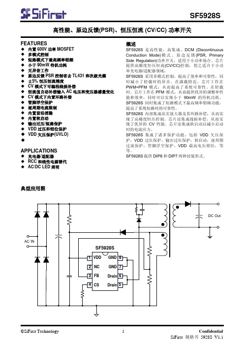
SFL659
特点
◆ 四分段开关调光(100%、50%、25%、12.5%调
光比)
◆ 内置650V 功率MOSFET
◆ 专利的“NC-Aux/PSR TM
”技术,省去供电绕
◆◆◆◆◆◆◆◆◆◆◆◆
◆概述
SFL659是超低成本、高精度、原边反馈LED 恒流功率开关,支持四分段开关调光(100%、50%、25%、12.5%调光比),适用于LED 照明领域。
SFL659采
用专利的“NC-Aux/PSR TM
”控制技术,可以省去供
四分段开关调光、NC-Aux/PSR TM LED 恒流功率开关
管脚封装
芯片内部模块图
电气参数
o
应用信息
SFL659是一个超低成本、无辅助绕组的工作于断续模式(DCM, Discontinuous Conduction Mode)、原边反馈(PSR, Primary Side Regulation)的功率开关,支持四分段开关调光(100%、50%、25%、12.5%调光比),芯片工作在脉冲频率调制PFM(PFM , Pulse Frequency Modulation)模式。
芯片集成的高精度恒流(CC, Constant Current)控制功能,以及诸
◆
在公式2中, Np 和 Ns 分别为变压器初级和次级的
匝数。
结合公式1和公式2,输出平均电流可以表示为:
dem S S
P pk o T f N N I I ××××=
21
(公式.3)
恒流(CC, Constant Current) 控制原理
从公式.3可以看出,有两种实现恒流的方法:一种是脉冲频率调制PFM ,这种控制方式是使原边电感电流的峰值保持恒定,同时让每个周期的消磁脉宽Tdem 与开关频率fs 的乘积为定值,也就是让消磁脉宽Tdem 与开关周期Ts 的比例保定值,这样就可以实现输出电流为定值,而且与线输入电压和变压开路发生时,输出电压会冲高,当检测的消磁时间小于设定的输出过压消磁时间时,触发输出过压OVP 保护,芯片进入自动重启保护模式。
当RI 脚悬空时,输出过压消磁时间典型值为5.5us ;当RI 短路到地时,输出过压消磁时间典型值为6.6us 。
为了防止在上电过程中因检测不到消磁而造成无法
正常开机,芯片设计有最大关断时间保证LED电源能够正常快速起机。
当RI脚悬空时,最大关断时间典型值为270us;当RI 短路到地时,最大关断时间典型值为325us。
◆极低芯片工作电流
SFL659的工作电流非常低,芯片内部功耗典型值为170uA。
极低的芯片工作电流提高了系统转换效率,同时降低了VDD电容的要求。
◆PFM 控制改善EMI性能
如上所述,SFL659 采用PFM控制。
PFM控制可以改善系统EMI性能,因为PFM属于变频控制,内置有频谱扩展功能。
◆前沿消隐
每次功率MOSFET开通时,电流检测电阻上会出现电流尖峰。
为了避免这种电流尖峰造成芯片误关断,芯片内置有前沿消隐(LEB,leading edge blanking)电路。
前沿消隐时间典型为550ns,在前沿消隐时间内,芯片内部的逐周期电流限制的比较器不会被误触发造成关断。
◆最小关断时间
SFL659集成了最小关断时间(OFF time)控制,典型为2us。
最小关断时间可以防止了功率开关关断初期的毛刺电压对芯片正常工作的干扰,尤其是当变压器漏感感量较大和输出电压较低时。
◆管脚浮空保护
在SFL659中,如果管脚浮空现象发生,芯片设计为进入保护模式,不会导致系统损坏。
◆自动重启保护
当某个保护被触发后,保护被锁存,同时芯片开关动作终止,并且通过芯片内部对VDD电容进行放电,使VDD掉电重启,启动结束后,芯片开始动作,并确认保护是否解除,如果保护未解除,芯片又进入保护锁存状态,并重复掉电重启,直至保护被解除。
◆智能热响应
在SFL659中内置智能热响应功能,当芯片过热时,芯片内部会逐渐增大关断时间,由于工作频率下降而降低输出功率和系统损耗,进而降低芯片温度,可以有效避免过温对芯片造成的损坏。
◆内部功率MOSFET的软驱动
SFL659 内置了一个软驱动级,软驱动方式改善了系统的EMI性能,实现了效率、可靠性和EMI的平衡。
封装信息
IMPORTANT NOTICE
SiFirst Technology Nanhai, Ltd (SiFirst) reserves the right to make corrections, modifications, enhancements, improvements and other changes to its products and services at any time and to discontinue any product or service without notice. Customers should obtain the latest relevant information before placing orders and should verify that such information is current and complete.
SiFirst warrants performance of its hardware products to the specifications applicable at the time of sale in accordance with SiFirst’s standard warranty. Testing and other quality control techniques are used to the extent SiFirst deems necessary to support this warranty. Except where mandated by government requirements, testing of all parameters of each product is not necessarily performed.
SiFirst assumes no liability for application assistance or customer product design. Customers are responsible for their products and applications using SiFirst’s components. To minimize the risks associated with customer products and applications, customers should provide adequate design and operating safeguards. Reproduction of SiFirst’s information in SiFirst’s data books or data sheets is permissible only if reproduction is without alteration and is accompanied by all associated warranties, conditions, limitations, and notices. Reproduction of this information with alteration is an unfair and deceptive business practice. SiFirst is not responsible or liable for such altered documentation. Information of third parties may be subject to additional restrictions.
Resale of SiFirst’s products or services with statements different from or beyond the parameters stated by SiFirst for that product or service voids all express and any implied warranties for the associated SiFirst’s product or service and is an unfair and deceptive business practice. SiFirst is not responsible or liable for any such statements.
SiFirst’s products are neither designed nor intended for use in military applications. SiFirst will not be held liable for any damages or claims resulting from the use of its products in military applications.
SiFirst’s products are not designed to be used as components in devices intended to support or sustain human life. SiFirst will not be held liable for any damages or claims resulting from the use of its products in medical applications.。