LT1085IT-5中文资料
- 格式:pdf
- 大小:143.60 KB
- 文档页数:12


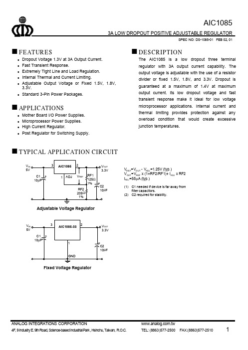
SPEC NO: DS-1085-01 FEB 02, 01n FEATURESl Dropout Voltage 1.3V at 3A Output Current.l Fast Transient Response.l Extremely Tight Line and Load Regulation.l Internal Thermal and Current Limiting.lAdjustable Output Voltage or Fixed 1.5V, 1.8V,3.3V.lStandard 3-Pin Power Packages.n APPLICATIONSl Mother Board I/O Power Supplies.l Microprocessor Power Supplies.l High Current Regulator.lPost Regulator for Switching Supply.n DESCRIPTIONThe AIC1085 is a low dropout three terminal regulator with 3A output current capability. The output voltage is adjustable with the use of a resistor divider or fixed 1.5V, 1.8V, and 3.3V. Dropout is guaranteed at a maximum of 1.4V at maximum output current. Its low dropout voltage and fast transient response make it ideal for low voltage microprocessor applications. Internal current and thermal limiting provides protection against any overload condition that would create excessive junction temperatures.n TYPICAL APPLICATION CIRCUITµF OUT V IN 5VV R E F =V OUT - V ADJ =1.25V (typ.)V OUT =V REF x (1+RF2/RF1)+ I ADJ x RF2I ADJ =55µA (typ.)(1) C1 needed if device is far away fromfilter capacitors.(2) C2 required for stability.Adjustable Voltage RegulatorµFOUT V 5VFixed Voltage RegulatorSPEC NO: DS-1085-01 FEB 02, 01 nn ABSOLUTE MAXIMUM RATINGSV in pin to ADJ/ GND pin (7V)O perating Junction Temperature Range..................………...................... 0°C~ 125°CS torage Temperature Range...............................………….................-65°C ~ 150°CT hermal Resistance Junction to Case TO-252…………………….…………… 15°C/WTO-263, TO-220………............………... 6°C /WT hermal Resistance Junction to Ambient TO-252…………………………..… 100°C/W(Assume no ambient airflow, no heatsink)TO-263….....…….....……………... 60°C /WTO-220…....……....……………….. 50°C /WL ead Temperature (Soldering) 10 sec......................………............……..….......260°Cn TEST CIRCUITR efer to TYPICAL APPLICATION CIRCUIT.SPEC NO: DS-1085-01 FEB 02, 01n ELECTRICAL CHARACTERISTICS (VIN=5V, T A =25°C, I O =10mA, Unless otherwisespecified)P ARAMETERT EST CONDITIONSM IN.T YP.M AX.U NITR eference Voltage (V OUT -V ADJ ) A IC1085 (Adj.)T A =25°C 1.238 1.25 1.262VO utput VoltageA IC1085-15 V IN =5VA IC1085-18 V IN =5VA IC1085-33 V IN =5V 1.48 1.78 3.26 1.50 1.803.30 1.52 1.82 3.34 V L ine RegulationA dj : 2.75V ≤ V IN ≤5.25V%F ix : V O UT +1V ≤ V IN ≤7VT A =25°C0.0150.2L oad Regulation 10mA < I O < 3AT A =25°C 0.6%D ropout Voltage∆V OUT , ∆V REF =1%10mA ≤ I O ≤3A0°C ≤T J ≤125°C 1.3 1.4VC urrent LimitV IN = 5V0°C ≤T J ≤125°C 3 4 AA djusted Pin Current (I ADJ )2.75V ≤ V IN ≤ 7V 55 120 µA Adjusted Pin Current Change (∆I ADJ )2.75V ≤ V IN ≤ 7V 0°C ≤T J ≤125°C0.25µAT emperature StabilityI O =0.5A0°C ≤T J ≤125°C 0.5 %M inimum Load Current0°C ≤T J ≤125°C 5 10 m AR MS Output Noise (% of V OUT )10Hz ≤ f ≤ 10KHz0.003%R ipple Rejection Ratio120Hz input rippleC OUT =25µF(V IN -V OUT )=3V 60 72d BSPEC NO: DS-1085-01 FEB 02, 01 n BLOCK DIAGRAMV INV OUTn PIN DESCRIPTIONSA DJ PIN-Providing V REF=1.25V (typ.) foradjustable V OUT. V REF=V OUT-V ADJand I ADJ=55µA (typ.)(GND PIN-Power Ground.)V OUT PIN-Adjustable output voltage. V IN PIN-Power Input.SPEC NO: DS-1085-01 FEB 02, 01n TYPICAL PERFORMANCE CHARACTERISTICSL o a d C u r r e n tTime (µS)04080120160200O u t p u t V o l t a g e (V , A C )Line Transient ResponseTime (µS)O u t p u t V o l t a g e (m V , A C )I np u t V o l t a g e (V )010********Dropout Voltage (VOUT=3.3V)Output Current (A)M i n i m u m D i f f e r e n t i a l V o l t a g e (V )0.00.51.01.52.02.53.01.061.081.101.121.141.161.181.201.22Minimum Operating CurrentDifferential Voltage (V)M i n i m u m O p e r a t i n g C u r r e n t (m A )123450.20.40.60.81.01.21.41.61.8SPEC NO: DS-1085-01 FEB 02, 01 n PHYSICAL DIMENSIONSl TO-220 (unit: mm)SYMBOL MIN MAXA 3.56 4.82D14.2316.51E9.6610.66e 2.29 2.79e10.50 1.15e2- 1.10F0.51 1.39J1 2.04 2.92L12.7014.73l TO-252 (unit: mm)SYMBOL MIN MAXA 2.19 2.38A1 1.02 1.27b0.640.88b2 5.21 5.46C10.460.58D 5.33 5.59E 6.35 6.73e 2.28 (TYP.)H9.4010.42A1L0.51-SPEC NO: DS-1085-01 FEB 02, 01l TO-263 (unit: mm)SYMBOLMIN MAX A4.06 4.83b 0.50 1.00b2 1.14 1.40C-0.7c2 1.14 1.40D 8.639.66E9.6510.29e2.54 (TYP.)L 14.6015.88L1 2.28 2.80AL2-1.40U NIT: mm。
12PARAMETER CONDITIONS MIN TYP MAX UNITS Load Regulation(V IN – V OUT) = 3V10mA ≤ I OUT≤ I FULL LOADT J = 25°C (Notes 2, 3, 4, 6)0.10.3%q0.20.4% Dropout Voltage∆V REF = 1%, I OUT = I FULLLOAD (Notes 5, 6, 8)q 1.3 1.5V Current LimitLT1083(V IN – V OUT) = 5V q8.09.5A(V IN – V OUT) = 25V q0.4 1.0A LT1084(V IN – V OUT) = 5V q 5.5 6.5A(V IN – V OUT) = 25V q0.30.6A LT1085(V IN – V OUT) = 5V q 3.2 4.0A(V IN – V OUT) = 25V q0.20.5A Minimum Load Current(V IN – V OUT) = 25V q510mA Thermal Regulation T A = 25°C, 30ms PulseLT10830.0020.010%/W LT10840.0030.015%/W LT10850.0040.020%/W Ripple Rejection f = 120Hz, C ADJ = 25µF, C OUT = 25µF TantalumI OUT = I FULL LOAD, (V IN – V OUT) = 3V (Notes 6, 7, 8)q6075dB Adjust Pin Current T J = 25°C55µAq120µA Adjust Pin Current Change10mA ≤ I OUT≤ I FULL LOAD1.5V ≤ (V IN – V OUT) ≤ 25V (Note 6)q0.25µA Temperature Stability q0.5% Long Term Stability T A = 125°C, 1000 Hrs0.31% RMS Output Noise (% of V OUT)T A = 25°C10Hz = ≤ f ≤ 10kHz0.003% Thermal Resistance Junction-to-Case Control Circuitry/Power TransistorLT1083K Package0.6/1.6°C/WP Package0.5/1.6°C/W LT1084K Package0.75/2.3°C/WP Package0.65/2.3°C/WT Package0.65/2.7°C/W LT1085K Package0.9/3.0°C/WM, T Packages0.7/3.0°C/W ELECTRICAL CHARACTERISTICSNote 1: Absolute Maximum Ratings are those values beyond which the life of a device may be impaired.Note 2: See thermal regulation specifications for changes in output voltage due to heating effects. Load and line regulation are measured at a constant junction temperature by low duty cycle pulse testing.Note 3: Line and load regulation are guaranteed up to the maximum power dissapation (60W for the LT1083, 45W for the LT1084 (K, P), 30W for the LT1084 (T) and 30W for the LT1085). Power dissipation is determined by the input/output differential and the output current. Guaranteed maximum power dissipation will not be available over the full input/output voltage range.Note 4: I FULL LOAD is defined in the current limit curves. The I FULLLOAD curve is defined as the minimum value of current limit as a function of input-to-output voltage. Note that the 60W power dissipation for theLT1083 (45W for the LT1084 (K, P), 30W for the LT1084 (T), 30W for the LT1085) is only achievable over a limited range of input-to-output voltage. Note 5: Dropout voltage is specified over the full output current range of the device. Test points and limits are shown on the Dropout Voltage curve.Note 6: For LT1083 I FULL LOAD is 5A for –55°C ≤ T J < –40°C and 7.5A for T J≥ –40°C.Note 7: 1.7V ≤ (V IN – V OUT) ≤ 25V for LT1084 at –55°C ≤ T J≤–40°C. Note 8: Dropout is 1.7V maximum for LT1084 at –55°C ≤ T J≤ –40°C.The q denotes the specifications which apply over the full operating temperature range, otherwise specifications are at T A = 25°C.345678910APPLICATIO S I FOR ATIO W UU U Connected as shown, R P is not multiplied by the divider ratio. R P is about 0.004Ω per foot using 16-gauge wire.This translates to 4mV/ft at 1A load current, so it is important to keep the positive lead between regulator and load as short as possible and use large wire or PC board traces.Thermal ConsiderationsThe LT1083 series of regulators have internal power and thermal limiting circuitry designed to protect the device under overload conditions. For continuous normal load conditions however, maximum junction temperature rat-ings must not be exceeded. It is important to give careful consideration to all sources of thermal resistance from junction to ambient. This includes junction-to-case, case-to-heat sink interface, and heat sink resistance itself. New thermal resistance specifications have been developed to more accurately reflect device temperature and ensure safe operating temperatures. The data section for these new regulators provides a separate thermal resistance and maximum junction temperature for both the Control Sec-tion and the Power Transistor . Previous regulators, with a single junction-to-case thermal resistance specification,used an average of the two values provided here and therefore could allow excessive junction temperatures under certain conditions of ambient temperature and heat sink resistance. To avoid this possibility, calculations should be made for both sections to ensure that both thermal limits are met.Junction-to-case thermal resistance is specified from the IC junction to the bottom of the case directly below the die.This is the lowest resistance path for heat flow. Proper mounting is required to ensure the best possible thermal flow from this area of the package to the heat sink. Thermalcompound at the case-to-heat sink interface is strongly recommended. If the case of the device must be electri-cally isolated, a thermally conductive spacer can be used,as long as its added contribution to thermal resistance is considered. Note that the case of all devices in this series is electrically connected to the output.For example, using an LT1083CK (TO-3, Commercial) and assuming:V IN (max continuous) = 9V, V OUT = 5V, I OUT = 6A,T A = 75°C, θHEAT SINK = 1°C/W,θCASE-TO-HEAT SINK = 0.2°C/W for K package with thermal compound.Power dissipation under these conditions is equal to:P D = (V IN – V OUT )(I OUT ) = 24W Junction temperature will be equal to:T J = T A + P D (θHEAT SINK + θCASE-TO-HEAT SINK + θJC )For the Control Section:T J = 75°C + 24W (1°C/W + 0.2°C/W + 0.6°C/W) = 118°C 118°C < 125°C = T JMAX (Control Section Commercial Range)For the Power Transistor:T J = 75°C + 24W (1°C/W + 0.2°C/W + 1.6°C/W) = 142°C 142°C < 150°C = T JMAX (Power Transistor Commercial Range)In both cases the junction temperature is below the maximum rating for the respective sections, ensuring reliable operation.11121314Information furnished by Linear Technology Corporation is believed to be accurate and reliable. However, no responsibility is assumed for its use. Linear Technology Corporation makes no represen-tation that the interconnection of its circuits as described herein will not infringe on existing patent rights.15161083fds, sn1083 LT/TP 0200 2K REV D • PRINTED IN USA© LINEAR TECHNOLOGY CORPORA TION 1994Linear Technology Corporation1630 McCarthy Blvd., Milpitas, CA 95035-7417(408) 432-1900 q FAX: (408) 434-0507 q 。
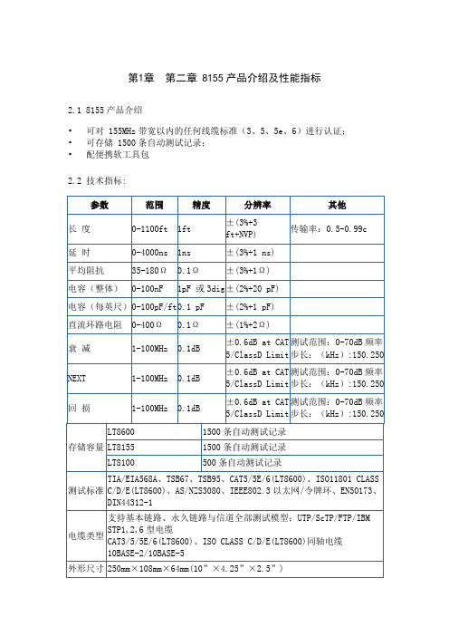
第1章第二章 8155产品介绍及性能指标2.1 8155产品介绍•可对 155MHz带宽以内的任何线缆标准(3、5、5e、6)进行认证;•可存储 1500条自动测试记录;•配便携软工具包2.2 技术指标:2.3 光纤测试选件·适用于LT8155/LT8600·可测多模和单模光纤系统的衰减值;·支持多种连接器类型·自动测试多种波长;·产生用于多模光纤的850nm和1300nm激光;·产生用于单模光纤的1310nm和1550nm激光;·测试结果可按测试方向、测试结果和工程名称进行分析保存·可用LT-Record Manager管理、分析软件存储并输出测试结果2.4 光纤选件技术指标第2章第三章 8155芯片结构3.1 8155的结构和引脚8155有40个引脚,采用双列直插封装,其引脚图和组成框图如图所示。
(1) 地址/数据线AD0~AD7(8条)(2) I/O口总线(22条):PA0~PA7、PB0~PB7、 PC0~PC5。
(3) 控制总线(8条)ALE ——地址锁存(输入)IO / /M—— IO口/RAM选择, 0:选内RAM; 1:选内IO口/CE ——片选线/RD、/WR ——读、写控制TIMERIN ——定时器输入(输入定时器所需时钟)TIMEROUT ——定时器输出(输出所产生的方波脉冲)3.2 8155的RAM和I / O口地址编码3.3 8155的工作方式与基本操作有三种基本操作:1、作单片机片外256B数据存储器IO / /M = 0,与其它数据存储器统一编址。
用MOVX访问。
2、作扩展I / O口使用IO / /M = 1,PA口、PB口、PC口,可通过编程决定如何使用。
1)命令寄存器(命令控制字)—— I / O口工作方式I / O口工作方式有四种:A口、B口基本I / O口, C口输入;A口、B口基本I / O口, C口输出;A口选通I / O、B口基本I / O、C口作联络线;A口、B口选通I / O、C口作联络线。
LT1085 — 3A 低压差正可调稳压器特点
•三端可调
•输出电流:3A、5A 或7.5A
•可在低至1V 的压差条件下运作
•在多种电流水平条件下提供保证的压差
•电压调整率:0.015%
•负载调整率:0.01%
•进行了全面的热限制功能测试
•可提供固定版本
•提供3 引脚塑料TO-220、TO-3P 和DD 封装
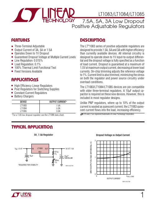
典型应用
描述
LT®1083 系列正可调稳压器专为以高于现有器件的效率来提供7.5A、5A 和3A 输出电流而设计。
所有内部电路均为能够在低至1V 的输入至输出差分电压条件下运作而设计,并且把压差电压作为负载电流的一个函数拟订了全面的规格。
压差在最大输出电流条件下保证为 1.5V (最大值),并在较低负载电流时有所减小。
片内修整把输出电压准确度调节至1%。
对电流限值也进行了修整,从而最大限度地减小了过载条件下稳压器和电源电路上承受的应力。
LT1083/LT1084/LT1085 器件的引脚与老式三端稳压器兼容。
在这些新型器件上需要布设一个10μF 输出电容器;然而,在大多数稳压器设计中通常已包括该电容器。
与PNP 稳压器(它有多达10% 的输出电流作为静态电流而消耗掉了) 的不同,LT1083 的静态电流将流入负载,从而提升了效率。
应用
•高效率线性稳压器
•用于开关电源的后置稳压器
•恒定电流稳压器
* 对于一个1.5A 的低压差稳压器,请参考LT1086 数据表。
3A LOW DROPOUT VOLTAGE REGULATOR (Adjustable & Fixed)LM1085● Powering VGA & Sound Card ORDERING INFORMATIONDevice & Marking PackageLM1085S-XX SOT 223LM1085T-XX TO263 (D2) DESCRIPTION(XX=Vout=1.5V, 2.5V, 2.85V, 3.0V, 3.3V, 5.0VAdjustable= AD)The LM1085 is a low dropout three terminal regulator with 3A output current capability.The output voltage is adjustable with the use of a resistor divider. Dropout is guaranteed at a maximumof 500 mV at maximum output current.It's low dropout voltage and fast transient response make it ideal for low voltage microprocessor applications. Internal current and thermal limiting provides protection against any overload conditionthat would create excessive junction temperature.TEST & TYPICAL APPLICATION CIRCUITHTC13A LOW DROPOUT VOLTAGE REGULATOR(ADJ)LM1085ABSOULTE MAXIMUM RATINSCHARACTERISTIC Supply VoltageOperating Junction Temperature Range Storage Temperature RangeThermal Resistance Junction to Case TO-263Thermal Resistance Junction to Ambient TO-263Lead Temperature (Soldering) 10 sec.Maximum Output CurrentELECTRICAL CHARACTERISTICS IOUT =100㎃, T A =25℃, unless otherwise specifiedMin. Load Current(Note 3) Line Regulation (ΔV REF (V IN )) Load Regulation (ΔV REF (V OUT )) Dropout Voltage Current Limit I OUT (MAX) Thermal Regulation (ΔV OUT (Pwr)) Output Noise, RMS HTC2VUNIT0<I OUT <3A, 2.75V<V IN <10V PARAMETEROutput Voltage TEST CONDITIONS Output Voltage Output Voltage 5.050<I OUT <3A, 3.5V<V IN <10V 2.85V Version Output Voltage 0<I OUT <3A, 4.35V<V IN <10V 2.821 2.85VV5.0V Version 0.2 Reference Voltage (V REF )VOutput Voltage All Voltage Options 0≤I OUT ≤3A, 5.5V≤V IN <10V V IN ≤7V,P≤P MAX1.5V≤(V IN-V OUT )≤5.75V, 10㎃≤I OUT ≤3A 4.9551.11.5V≤(V IN-V OUT )≤5.75V2.75V≤V IN ≤7V, I OUT =10㎃, T J =25℃ 10㎃≤I OUT ≤3A,(V IN -V OUT )=3V,T J =25℃ ΔV REF =1% , Iout=3A mA %5100.005%/Vo℃/W℃%/W %%V 0.31.2V Imax33.0V Version Output Voltage 0<I OUT <3A,4.5V<V IN <10V 2.973 3.03 2.5V Version VTja 60Tsol 300Tjc 3Vin 7Topr 0~125 3.3V Version 1.5V Version 0<I OUT <3A, 4.75V<V IN <10V 2.5 2.5253.267 3.3 3.333V2.8781.2380.0031.25 1.2631.2251.25 1.270.050.01Long Term Stability T A =25℃, 30㎳ pulse Vin-Vout=3V1.4V≤(V IN -V OUT ) Adjustable Only Thermal ResistanceJunction to Tab Junction to AmbientT A =125℃, 1000Hrs 10Hz to 10Khz T A =25℃30.0260MIN TYP MAX 1.485 1.5 1.5152.475A0.313.2 4.0C/W C/W ℃ASYMBOL Tstg -65~150UNIT V ℃VALUE。