SPI接口以太网控制器ENC28J60及其应用
- 格式:doc
- 大小:183.00 KB
- 文档页数:7
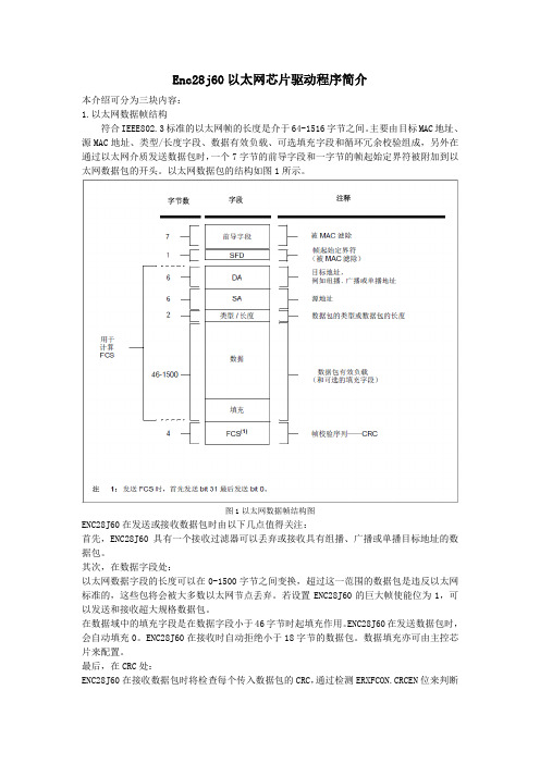
Enc28j60以太网芯片驱动程序简介本介绍可分为三块内容:1.以太网数据帧结构符合IEEE802.3标准的以太网帧的长度是介于64-1516字节之间。
主要由目标MAC地址、源MAC地址、类型/长度字段、数据有效负载、可选填充字段和循环冗余校验组成,另外在通过以太网介质发送数据包时,一个7字节的前导字段和一字节的帧起始定界符被附加到以太网数据包的开头。
以太网数据包的结构如图1所示。
图1以太网数据帧结构图ENC28J60在发送或接收数据包时由以下几点值得关注:首先,ENC28J60具有一个接收过滤器可以丢弃或接收具有组播、广播或单播目标地址的数据包。
其次,在数据字段处:以太网数据字段的长度可以在0-1500字节之间变换,超过这一范围的数据包是违反以太网标准的,这些包将会被大多数以太网节点丢弃。
若设置ENC28J60的巨大帧使能位为1,可以发送和接收超大规格数据包。
在数据域中的填充字段是在数据字段小于46字节时起填充作用。
ENC28J60在发送数据包时,会自动填充0。
ENC28J60在接收时自动拒绝小于18字节的数据包。
数据填充亦可由主控芯片来配置。
最后,在CRC处:ENC28J60在接收数据包时将检查每个传入数据包的CRC,通过检测ERXFCON.CRCEN位来判断输入数据包的CRC是否正确。
ENC28J60在发送数据包时,将自动生成一个有效的CRC并发送它。
发送数据包的CRC亦可由主控芯片来提供。
2.驱动程序介绍(1)ENC28J60的寄存器读写规则由于ENC28J60芯片采用的是SPI串行接口模式,其对内部寄存器读写的规则是先发操作码<前3bit>+寄存器地址<后5bit>,再发送欲操作数据。
通过不同操作码来判别操作时读寄存器(缓存区)还是写寄存器(缓冲区)或是其它。
(2)ENC28J60芯片初始化程序ENC28J60发送和接收数据包前必须对内进行初始化设置,通常在复位后完成,不需再更改。
ENC28J60Data SheetStand-Alone Ethernet Controllerwith SPI Interface © 2008 Microchip Technology Inc.Preliminary DS39662CDS39662C-page iiPreliminary© 2008 Microchip Technology Inc.Information contained in this publication regarding device applications and the like is provided only for your convenience and may be superseded by updates. It is your responsibility to ensure that your application meets with your specifications.MICROCHIP MAKES NO REPRESENTATIONS OR WARRANTIES OF ANY KIND WHETHER EXPRESS OR IMPLIED, WRITTEN OR ORAL, STATUTORY OR OTHERWISE, RELATED TO THE INFORMATION,INCLUDING BUT NOT LIMITED TO ITS CONDITION,QUALITY , PERFORMANCE, MERCHANTABILITY OR FITNESS FOR PURPOSE . Microchip disclaims all liability arising from this information and its use. Use of Microchip devices in life support and/or safety applications is entirely at the buyer’s risk, and the buyer agrees to defend, indemnify and hold harmless Microchip from any and all damages, claims,suits, or expenses resulting from such use. No licenses are conveyed, implicitly or otherwise, under any Microchip intellectual property rights.TrademarksThe Microchip name and logo, the Microchip logo, Accuron, dsPIC, K EE L OQ , K EE L OQ logo, MPLAB, PIC, PICmicro,PICSTART, PRO MATE, rfPIC and SmartShunt are registered trademarks of Microchip Technology Incorporated in the U.S.A. and other countries.FilterLab, Linear Active Thermistor, MXDEV, MXLAB,SEEVAL, SmartSensor and The Embedded Control Solutions Company are registered trademarks of Microchip Technology Incorporated in the U.S.A.Analog-for-the-Digital Age, Application Maestro, CodeGuard, dsPICDEM, , dsPICworks, dsSPEAK, ECAN, ECONOMONITOR, FanSense, In-Circuit SerialProgramming, ICSP , ICEPIC, Mindi, MiWi, MPASM, MPLAB Certified logo, MPLIB, MPLINK, mTouch, PICkit, PICDEM, , PICtail, PIC 32 logo, PowerCal, PowerInfo,PowerMate, PowerTool, REAL ICE, rfLAB, Select Mode, Total Endurance, UNI/O, WiperLock and ZENA are trademarks of Microchip Technology Incorporated in the U.S.A. and other countries.SQTP is a service mark of Microchip Technology Incorporated in the U.S.A.All other trademarks mentioned herein are property of their respective companies.© 2008, Microchip Technology Incorporated, Printed in the U.S.A., All Rights Reserved.Printed on recycled paper.Note the following details of the code protection feature on Microchip devices:•Microchip products meet the specification contained in their particular Microchip Data Sheet.•Microchip believes that its family of products is one of the most secure families of its kind on the market today, when used in the intended manner and under normal conditions.•There are dishonest and possibly illegal methods used to breach the code protection feature. All of these methods, to ourknowledge, require using the Microchip products in a manner outside the operating specifications contained in Microchip’s Data Sheets. Most likely, the person doing so is engaged in theft of intellectual property.•Microchip is willing to work with the customer who is concerned about the integrity of their code.•Neither Microchip nor any other semiconductor manufacturer can guarantee the security of their code. Code protection does not mean that we are guaranteeing the product as “unbreakable.”Code protection is constantly evolving. We at Microchip are committed to continuously improving the code protection features of our products. Attempts to break Microchip’s code protection feature may be a violation of the Digital Millennium Copyright Act. If such acts allow unauthorized access to your software or other copyrighted work, you may have a right to sue for relief under that Act.Microchip received ISO/TS-16949:2002 certification for its worldwide headquarters, design and wafer fabrication facilities in Chandler and Tempe, Arizona; Gresham, Oregon and design centers in California and India. The Company’s quality system processes and procedures are for its PIC ® MCUs and dsPIC ® DSCs, K EE L OQ ® code hoppingdevices, Serial EEPROMs, microperipherals, nonvolatile memory and analog products. In addition, Microchip’s quality system for the design and manufacture of development systems is ISO 9001:2000 certified.ENC28J60Ethernet Controller Features•IEEE 802.3™ Compatible Ethernet Controller •Fully Compatible with 10/100/1000Base-T Networks •Integrated MAC and 10Base-T PHY•Supports One 10Base-T Port with Automatic Polarity Detection and Correction•Supports Full and Half-Duplex modes •Programmable Automatic Retransmit on Collision •Programmable Padding and CRC Generation •Programmable Automatic Rejection of Erroneous Packets•SPI Interface with Clock Speeds Up to 20MHz Buffer•8-Kbyte Transmit/Receive Packet Dual Port SRAM •Configurable Transmit/Receive Buffer Size •Hardware Managed Circular Receive FIFO•Byte-Wide Random and Sequential Access with Auto-Increment•Internal DMA for Fast Data Movement •Hardware Assisted Checksum Calculation for Various Network ProtocolsMedium Access Controller (MAC) Features•Supports Unicast, Multicast and Broadcast Packets•Programmable Receive Packet Filtering and Wake-up Host on Logical AND or OR of the Following:-Unicast destination address-Multicast address-Broadcast address-Magic Packet™-Group destination addresses as defined by64-bit Hash Table-Programmable Pattern Matching of up to64bytes at user-defined offsetPhysical Layer (PHY) Features•Loopback mode•Two Programmable LED Outputs for LINK, TX, RX, Collision and Full/Half-Duplex Status Operational•Six Interrupt Sources and One Interrupt Output Pin •25MHz Clock Input Requirement•Clock Out Pin with Programmable Prescaler •Operating Voltage of 3.1V to 3.6V (3.3V typical)•5V Tolerant Inputs•Temperature Range: -40°C to +85°C Industrial, 0°C to +70°C Commercial (SSOP only)•28-Pin SPDIP, SSOP, SOIC, QFN PackagesStand-Alone Ethernet Controller with SPI Interface© 2008 Microchip Technology Inc.Preliminary DS39662C-page 1ENC28J60Table of Contents1.0Overview (3)2.0External Connections (5)3.0Memory Organization (11)4.0Serial Peripheral Interface (SPI) (25)5.0Ethernet Overview (31)6.0Initialization (33)7.0Transmitting and Receiving Packets (39)8.0Receive Filters (47)9.0Duplex Mode Configuration and Negotiation (53)10.0Flow Control (55)11.0Reset (59)12.0Interrupts (63)13.0Direct Memory Access Controller (71)14.0Power-Down (73)15.0Built-in Self-Test Controller (75)16.0Electrical Characteristics (79)17.0Packaging Information (83)Appendix A: Revision History (89)The Microchip Web Site (91)Customer Change Notification Service (91)Customer Support (91)Reader Response (92)Index (93)Product Identification System (95)TO OUR VALUED CUSTOMERSIt is our intention to provide our valued customers with the best documentation possible to ensure successful use of your Microchip products. To this end, we will continue to improve our publications to better suit your needs. Our publications will be refined and enhanced as new volumes and updates are introduced.If you have any questions or comments regarding this publication, please contact the Marketing Communications Department via E-mail at docerrors@ or fax the Reader Response Form in the back of this data sheet to (480) 792-4150. We welcome your feedback.Most Current Data SheetTo obtain the most up-to-date version of this data sheet, please register at our Worldwide Web site at:You can determine the version of a data sheet by examining its literature number found on the bottom outside corner of any page. The last character of the literature number is the version number, (e.g., DS30000A is version A of document DS30000).ErrataAn errata sheet, describing minor operational differences from the data sheet and recommended workarounds, may exist for current devices. As device/documentation issues become known to us, we will publish an errata sheet. The errata will specify the revision of silicon and revision of document to which it applies.To determine if an errata sheet exists for a particular device, please check with one of the following:•Microchip’s Worldwide Web site; •Your local Microchip sales office (see last page)When contacting a sales office, please specify which device, revision of silicon and data sheet (include literature number) you are using.Customer Notification SystemRegister on our web site at to receive the most current information on all of our products.DS39662C-page 2Preliminary© 2008 Microchip Technology Inc.© 2008 Microchip Technology Inc.PreliminaryDS39662C-page 3ENC28J601.0OVERVIEWThe ENC28J60 is a stand-alone Ethernet controller with an industry standard Serial Peripheral Interface (SPI). It is designed to serve as an Ethernet network interface for any controller equipped with SPI.The ENC28J60 meets all of the IEEE 802.3 specifica-tions. It incorporates a number of packet filtering schemes to limit incoming packets. It also provides an internal DMA module for fast data throughput and hard-ware assisted checksum calculation, which is used in various network protocols. Communication with the host controller is implemented via an interrupt pin and the SPI, with clock rates of up to 20MHz. Two dedicated pins are used for LED link and network activity indication.A simple block diagram of the ENC28J60 is shown in Figure 1-1. A typical application circuit using the device is shown in Figure 1-2. With the ENC28J60, two pulse transformers and a few passive components are all that are required to connect a microcontroller to an Ethernet network.The ENC28J60 consists of seven major functional blocks:1.An SPI interface that serves as a communica-tion channel between the host controller and the ENC28J60.2.Control registers which are used to control and monitor the ENC28J60.3. A dual port RAM buffer for received and transmitted data packets.4.An arbiter to control the access to the RAM buffer when requests are made from DMA,transmit and receive blocks.5.The bus interface that interprets data and commands received via the SPI interface.6.The MAC (Medium Access Control) module that implements IEEE 802.3 compliant MAC logic.7.The PHY (Physical Layer) module that encodes and decodes the analog data that is present on the twisted-pair interface.The device also contains other support blocks, such as the oscillator, on-chip voltage regulator, level translators to provide 5V tolerant I/Os and system control logic.FIGURE 1-1:ENC28J60 BLOCK DIAGRAMDual Port RAM8 Kbytes DMA &ChecksumTXBMRXBMArbiterFlow Control Host InterfaceControl Registers25 MHz Power-on PHYBus InterfaceSPIMII InterfaceMIIM InterfaceTPOUT+TPOUT-TPIN+TPIN-TXRXRBIASOSC1OSC2Voltage System ControlCS (1)SI (1)SO SCK (1)INTV CAPCLKOUTLEDA LEDBRESET (1)RXF (Filter)RXTXMACch0ch1ch0ch1Buffer Note 1:These pins are 5V tolerant.RegulatorResetOscillatorENC28J60DS39662C-page 4Preliminary© 2008 Microchip Technology Inc.FIGURE 1-2:TYPICAL ENC28J60-BASED INTERFACETABLE 1-1:PINOUT I/O DESCRIPTIONSPin Name Pin NumberPin Type Buffer Type DescriptionSPDIP , SOIC, SSOPQFN V CAP125P—2.5V output from internal regulator. A low Equivalent Series Resistance (ESR) capacitor, with a typical value of 10 mF and a minimum value of 1mF to ground, must be placed on this pin.V SS 226P —Ground reference.CLKOUT 327O —Programmable clock output pin.(1) INT 428O —INT interrupt output pin.(2)NC 51O —Reserved function; always leave unconnected.SO 62O —Data out pin for SPI interface.(2) SI 73I ST Data in pin for SPI interface.(3) SCK 84I ST Clock in pin for SPI interface.(3)CS 95I ST Chip select input pin for SPI interface.(3,4) RESET 106I ST Active-low device Reset input.(3,4) V SSRX 117P —Ground reference for PHY RX.TPIN-128I ANA Differential signal input.TPIN+139I ANA Differential signal input.RBIAS1410IANABias current pin for PHY . Must be tied to ground via a resistor (refer toSection 2.4 “Magnetics, Termination and Other External Components” for details).V DDTX 1511P —Positive supply for PHY TX.TPOUT-1612O —Differential signal output.TPOUT+1713O —Differential signal output.V SSTX 1814P —Ground reference for PHY TX.V DDRX 1915P —Positive 3.3V supply for PHY RX.V DDPLL 2016P —Positive 3.3V supply for PHY PLL.V SSPLL 2117P —Ground reference for PHY PLL.V SSOSC 2218P —Ground reference for oscillator.OSC12319I ANA Oscillator input.OSC22420O —Oscillator output.V DDOSC 2521P —Positive 3.3V supply for oscillator.LEDB 2622O —LEDB driver pin.(5) LEDA 2723O —LEDA driver pin.(5) V DD 2824P—Positive 3.3V supply.Legend:I = Input, O = Output, P = Power, ANA = Analog Signal Input, ST = Schmitt Trigger Note 1:Pins have a maximum current capacity of 8mA.2:Pins have a maximum current capacity of 4mA.3:Pins are 5V tolerant.4:Pins have an internal weak pull-up to V DD .5:Pins have a maximum current capacity of 12mA.TRANSFORMERMCUTX/RX BufferMACPHYLEDA LEDBSI SO SCKINTSDO SDI SCKINT XENC28J60TPIN+/-TPOUT+/-ETHERNET RJ45I/O CS© 2008 Microchip Technology Inc.PreliminaryDS39662C-page 5ENC28J602.0EXTERNAL CONNECTIONS2.1OscillatorThe ENC28J60 is designed to operate at 25MHz with a crystal connected to the OSC1 and OSC2 pins. The ENC28J60 design requires the use of a parallel cut crystal. Use of a series cut crystal may give a frequency out of the crystal manufacturer specifications. A typical oscillator circuit is shown in Figure 2-1.The ENC28J60 may also be driven by an external clock source connected to the OSC1 pin as shown in Figure 2-2.FIGURE 2-1:CRYSTAL OSCILLATOR OPERATIONFIGURE 2-2:EXTERNAL CLOCK SOURCE (1)2.2Oscillator Start-up TimerThe ENC28J60 contains an Oscillator Start-up Timer (OST) to ensure that the oscillator and integrated PHY have stabilized before use. The OST does not expire until 7500 OSC1 clock cycles (300μs) pass after Power-on Reset or wake-up from Power-Down mode occurs. During the delay, all Ethernet registers and buffer memory may still be read and written to through the SPI bus. However, software should not attempt to transmit any packets (set ECON1.TXRTS), enable reception of packets (set ECON1.RXEN) or access any MAC, MII or PHY registers during this period. When the OST expires, the CLKRDY bit in the ESTAT register will be set. The application software should poll this bit as necessary to determine when normal device operation can begin.C 1C 2XTALOSC2R S (1)OSC1R F (2)To Internal LogicNote 1:A series resistor, R S , may be required for AT strip cut crystals.2:The feedback resistor, R F , is typically in the range of 2 to 10M Ω.ENC28J603.3V Clock from External SystemOSC1OSC2Open (2)Note 1:Duty cycle restrictions must be observed.2:A resistor to ground may be used to reduce system noise. This may increase system current.ENC28J60Note:After a Power-on Reset, or the ENC28J60is removed from Power-Down mode, the CLKRDY bit must be polled before transmitting packets, enabling packet reception or accessing any MAC, MII or PHY registers.ENC28J60DS39662C-page 6Preliminary© 2008 Microchip Technology Inc.2.3CLKOUT PinThe clock out pin is provided to the system designer for use as the host controller clock or as a clock source for other devices in the system. The CLKOUT has an internal prescaler which can divide the output by 1, 2,3, 4 or 8. The CLKOUT function is enabled and the prescaler is selected via the ECOCON register (Register 2-1).To create a clean clock signal, the CLKOUT pin is held low for a period when power is first applied. After the Power-on Reset ends, the OST will begin counting.When the OST expires, the CLKOUT pin will begin out-putting its default frequency of 6.25MHz (main clock divided by 4). At any future time that the ENC28J60 is reset by software or the RESET pin, the CLKOUT func-tion will not be altered (ECOCON will not changevalue). Additionally, Power-Down mode may be entered and the CLKOUT function will continue to operate. When Power-Down mode is cancelled, the OST will be reset but the CLKOUT function will continue. When the CLKOUT function is disabled (ECOCON = 0), the CLKOUT pin is driven low. The CLKOUT function is designed to ensure that mini-mum timings are preserved when the CLKOUT pin function is enabled, disabled or the prescaler value is changed. No high or low pulses will be outputted which exceed the frequency specified by the ECOCON configuration. However, when switching frequencies, a delay between two and eight OSC1 clock periods will occur where no clock pulses will be produced (see Figure 2-3). During this period, CLKOUT will be held low.FIGURE 2-3:CLKOUT TRANSITIONECOCON Changed80 ns to 320 ns DelayREGISTER 2-1:ECOCON: CLOCK OUTPUT CONTROL REGISTERU-0U-0U-0U-0U-0R/W-1R/W-0R/W-0—————COCON2COCON1COCON0bit 7bit 0Legend:R = Readable bit W = Writable bit U = Unimplemented bit, read as ‘0’-n = Value at POR ‘1’ = Bit is set‘0’ = Bit is clearedx = Bit is unknownbit 7-3Unimplemented : Read as ‘0’bit 2-0COCON2:COCON0: Clock Output Configuration bits11x = Reserved for factory test. Do not use. Glitch prevention not assured.101 = CLKOUT outputs main clock divided by 8 (3.125 MHz)100 = CLKOUT outputs main clock divided by 4 (6.25 MHz)011 = CLKOUT outputs main clock divided by 3 (8.333333 MHz)010 = CLKOUT outputs main clock divided by 2 (12.5 MHz)001 = CLKOUT outputs main clock divided by 1 (25 MHz)000 = CLKOUT is disabled. The pin is driven low.© 2008 Microchip Technology Inc.PreliminaryDS39662C-page 7ENC28J602.4Magnetics, Termination and Other External ComponentsTo complete the Ethernet interface, the ENC28J60requires several standard components to be installed externally. These components should be connected as shown in Figure 2-4.The internal analog circuitry in the PHY module requires that an external 2.32 k Ω, 1% resistor be attached from RBIAS to ground. The resistor influences the TPOUT+/-signal amplitude. The resistor should be placed as close as possible to the chip with no immediately adjacent signal traces to prevent noise capacitively coupling into the pin and affecting the transmit behavior. It is recommended that the resistor be a surface mount type.Some of the device’s digital logic operates at a nominal 2.5V. An on-chip voltage regulator is incorporated to generate this voltage. The only external component required is an external filter capacitor, connected from V CAP to ground. The capacitor must have low equiva-lent series resistance (ESR), with a typical value of 10μF, and a minimum value of 1μF. The internal regulator is not designed to drive external loads.On the TPIN+/TPIN- and TPOUT+/TPOUT- pins,1:1center taped pulse transformers, rated for Ethernet operations, are required. When the Ethernet module is enabled, current is continually sunk through both TPOUT pins. When the PHY is actively transmitting, a differential voltage is created on the Ethernet cable by varying the relative current sunk by TPOUT+ compared to TPOUT-.A common-mode choke on the TPOUT interface, placed between the TPOUT pins and the Ethernet transformer (not shown), is not recommended. If a common-mode choke is used to reduce EMI emissions, it should be placed between the Ethernet transformer and pins 1 and 2 of the RJ-45 connector. Many Ethernet transformer modules include common-mode chokes inside the same device package. The transformers should have at least the isolation rating specified in Table 16-5 to protect against static voltages and meet IEEE 802.3 isolation requirements (see Section 16.0 “Electrical Character-istics” for specific transformer requirements). Both transmit and receive interfaces additionally require two resistors and a capacitor to properly terminate the transmission line, minimizing signal reflections. All power supply pins must be externally connected to the same power source. Similarly, all ground refer-ences must be externally connected to the same ground node. Each V DD and V SS pin pair should have a 0.1μF ceramic bypass capacitor (not shown in the schematic) placed as close to the pins as possible.Since relatively high currents are necessary to operate the twisted-pair interface, all wires should be kept as short as possible. Reasonable wire widths should be used on power wires to reduce resistive loss. If the differential data lines cannot be kept short, they should be routed in such a way as to have a 100Ω characteristic impedance.FIGURE 2-4:ENC28J60 ETHERNET TERMINATION AND EXTERNAL CONNECTIONSI/O SCK SDO SDIINT0MCULevel Shift Logic (2)CS SCK SI SOINTENC28J60V CAPLEDALEDBRBIASTPOUT +TPOUT -TPIN +TPIN -10μFNote 1:Ferrite Bead should be rated for at least 80mA.2:Required only if the microcontroller is operating at 5V. See Section 2.5 “I/O Levels” for more information.3:These components are installed for EMI reduction purposes.Ferrite Bead (1,3)3.3V2.32 k Ω, 1%12345678RJ-451:1 CT1:1 CT1 nF,2 kV (3)75Ω(3)75Ω(3)75Ω(3)75Ω(3)49.9Ω, 1%49.9Ω, 1%49.9Ω, 1%49.9Ω, 1%0.1 μF (3)0.1 μF1ENC28J60DS39662C-page 8Preliminary© 2008 Microchip Technology Inc.2.5I/O LevelsThe ENC28J60 is a 3.3V part; however, it was designed to be easily integrated into 5V systems. The SPI CS, SCK and SI inputs, as well as the RESET pin,are all 5V tolerant. On the other hand, if the host controller is operated at 5V, it quite likely will not be within specifications when its SPI and interrupt inputs are driven by the 3.3V CMOS outputs on the ENC28J60. A unidirectional level translator would be necessary.An economical 74HCT08 (quad AND gate), 74ACT125(quad 3-state buffer) or many other 5V CMOS chips with TTL level input buffers may be used to provide the necessary level shifting. The use of 3-state buffers permits easy integration into systems which share the SPI bus with other devices. Figure 2-5 and Figure 2-6show example translation schemes.FIGURE 2-5:LEVEL SHIFTING USING AND GATESFIGURE 2-6:LEVEL SHIFTING USING 3-STATE BUFFERS2.6LED ConfigurationThe LEDA and LEDB pins support automatic polarity detection on Reset. The LEDs can be connected such that the pin must source current to turn the LED on, or alternately connected such that the pin must sink cur-rent to turn the LED on. Upon system Reset, the ENC28J60 will detect how the LED is connected and begin driving the LED to the default state configured by the PHLCON register. If the LED polarity is changed while the ENC28J60 is operating, the new polarity will not be detected until the next system Reset occurs. LEDB is unique in that the connection of the LED is automatically read on Reset and determines how to initialize the PHCON1.PDPXMD bit. If the pin sources current to illuminate the LED, the bit is cleared on Reset and the PHY defaults to half-duplex operation. If the pin sinks current to illuminate the LED, the bit is set on Reset and the PHY defaults to full-duplex operation.Figure 2-7 shows the two available options. If no LED is attached to the LEDB pin, the PDPXMD bit will reset to an indeterminate value.FIGURE 2-7:LEDB POLARITY AND RESET CONFIGURATION OPTIONSThe LEDs can also be configured separately to control their operating polarity (on or off when active), blink rate and blink stretch interval. The options are controlled by the LACFG3:LACFG0 and LBCFG3:LBCFG0 bits.Typical values for blink stretch are listed in Table 2-1.TABLE 2-1:LED BLINK STRETCH LENGTHI/O SCK SOSI INT0MCUCS SCK SISO INTENC28J60CLKOUT OSC1I/O SCK SO SI INT0MCUCS SCK SI SO INTENC28J60CLKOUT OSC1Stretch Length Typical Stretch (ms)T NSTRCH (normal)40T MSTRCH (medium)70T LSTRCH (long)140LEDB+3.3VFull-Duplex Operation:PDPXMD = 1LEDBHalf-Duplex Operation:PDPXMD = 0REGISTER 2-2:PHLCON: PHY MODULE LED CONTROL REGISTERR/W-0R/W-0R/W-1R/W-1R/W-0R/W-1R/W-0R/W-0 r r r r LACFG3LACFG2LACFG1LACFG0 bit 15bit 8R/W-0R/W-0R/W-1R/W-0R/W-0R/W-0R/W-1R/W-x LBCFG3LBCFG2LBCFG1LBCFG0LFRQ1LFRQ0STRCH rbit 7bit 0Legend:R = Readable bit W = Writable bit U = Unimplemented bit, read as ‘0’-n = Value at POR‘1’ = Bit is set‘0’ = Bit is cleared x = Bit is unknownbit 15-14Reserved: Write as ‘0’bit 13-12Reserved: Write as ‘1’bit 11-8LACFG3:LACFG0: LEDA Configuration bits1111 = Reserved1110 = Display duplex status and collision activity (always stretched)1101 = Display link status and transmit/receive activity (always stretched)1100 = Display link status and receive activity (always stretched)1011 = Blink slow1010 = Blink fast1001 = Off1000 = On0111 = Display transmit and receive activity (stretchable)0110 = Reserved0101 = Display duplex status0100 = Display link status0011 = Display collision activity (stretchable)0010 = Display receive activity (stretchable)0001 = Display transmit activity (stretchable)0000 = Reservedbit 7-4LBCFG3:LBCFG0: LEDB Configuration bits1110 = Display duplex status and collision activity (always stretched)1101 = Display link status and transmit/receive activity (always stretched)1100 = Display link status and receive activity (always stretched)1011 = Blink slow1010 = Blink fast1001 = Off1000 = On0111 = Display transmit and receive activity (stretchable)0110 = Reserved0101 = Display duplex status0100 = Display link status0011 = Display collision activity (stretchable)0010 = Display receive activity (stretchable)0001 = Display transmit activity (stretchable)0000 = Reservedbit 3-2LFRQ1:LFRQ0: LED Pulse Stretch Time Configuration bits (see Table2-1)11 = Reserved10 = Stretch LED events by T LSTRCH01 = Stretch LED events by T MSTRCH00 = Stretch LED events by T NSTRCHbit 1STRCH: LED Pulse Stretching Enable bit1 =Stretchable LED events will cause lengthened LED pulses based on LFRQ1:LFRQ0 configuration0 =Stretchable LED events will only be displayed while they are occurringbit 0Reserved: Write as ‘0’NOTES:3.0MEMORY ORGANIZATIONAll memory in the ENC28J60 is implemented as static RAM. There are three types of memory in the ENC28J60:•Control Registers •Ethernet Buffer •PHY RegistersThe Control registers’ memory contains the registers that are used for configuration, control and status retrieval of the ENC28J60. The Control registers are directly read and written to by the SPI interface.The Ethernet buffer contains transmit and receive memory used by the Ethernet controller in a single memory space. The sizes of the memory areas are programmable by the host controller using the SPI interface. The Ethernet buffer memory can only be accessed via the read buffer memory and write buffer memory SPI commands (see Section 4.2.2 “Read Buffer Memory Command” and Section 4.2.4 “Write Buffer Memory Command”).The PHY registers are used for configuration, control and status retrieval of the PHY module. The registers are not directly accessible through the SPI interface;they can only be accessed through Media Independent Interface Management (MIIM) implemented in the MAC.Figure 3-1 shows the data memory organization for the ENC28J60.FIGURE 3-1:ENC28J60 MEMORY ORGANIZATIONCommon RegistersCommon RegistersCommon RegistersCommon Registers00h19h 1Ah 1Fh 00h19h 1Ah 1Fh 00h19h 1Ah 1Fh 00h19h 1Ah 1FhBank 0Bank 1Bank 2Bank 30000h1FFFh= 00= 01= 10= 11ECON1<1:0>Control Registers Ethernet Buffer00h 1FhPHY RegistersNote:Memory areas are not shown to scale. The size of the control memory space has been scaled to show detail.Buffer Pointers in Bank 0。

ENC28J60以太网模块用户手册V1.1目录一、功能特点 (2)二、硬件参数 (3)2.1外观 (3)2.2参数 (3)2.3软件支持 (3)2.4产品清单 (4)2.5典型应用 (4)三、模块配置 (5)3.1模块SPI接口说明 (5)3.2模块供电电压设置 (5)3.3通信接口电平设置 (5)四、原理图 (6)一、功能特点ENC28J60以太网模块是为方便单片机系统实现以太网通信而开发的独立模块。
该模块采用的ENC28J60芯片是带有行业标准串行外设接口(Serial Peripheral Interface,SPI)的独立以太网控制器。
ENC28J60符合IEEE802.3的全部规范,采用了一系列包过滤机制以对传入数据包进行限制。
它还提供了一个内部DMA模块,以实现快速数据吞吐和硬件支持的IP校验和计算。
与主控制器的通信通过两个中断引脚和SPI实现,数据传输速率高达10Mb/s。
两个专用的引脚用于连接LED,进行网络活动状态指示。
ENC28J60芯片工作电压范围是3.14V到3.45V,故不能直接于5V供电的MCU通信,该模块采用74AHC125高速三态缓存器实现了电平转换功能,并可通过跳线帽快速设置通信接口的电平类型,方便快速实现与各种电压类型的MCU通信。
模块输入电压类型为3.3V或5V,可通过跳线帽来设置。
二、硬件参数2.1外观2.2参数符合IEEE802.3的全部规范;集成MAC和10BASE-T PHY;SPI通信的最高数据传输速率高达10Mb/s;供电电压为3.3V或5V,可通过跳线帽来设置;与单片机通信的接口电平为3.3V或5V,可通过跳线帽来设置;内置网络变压器的RJ45以太网接口;工作温度::-40°C到+85°C(工业级);模块尺寸:54*33.5*1.6mm;2.3软件支持提供PIC及AVR芯片的TCP/IP协议栈,方便快速建立单片机的以太网通信应用。

SPI接口以太网控制器ENCJ及其应用————————————————————————————————作者:————————————————————————————————日期:SPI接口以太网控制器ENC28J60及其应用文章发布人:gxy 共36人阅读文字大小:[ 大中小 ] 文字背景色:Ethernet Controller with SPI™ Interface ENC28J60 and Its ApplicationAbstract: Today,most of the Ethernet controller is designed for personal computer, so its applying is much complicated。
The mode of extending bus is often needed. This paper introduces the world’s smallest package Ethernet controller ENC28J60 at present. Adopting the SPI serial interface mode, so the designing process is predigested. In this paper, it is introduced of the characters, inside structure and PIN function of Ethernet controller ENC28J60. Further more, the paper analyzes the setting of register and process of work in detail and illustrates the application circuit with the interface of MCU.Key Words: Ethernet controller; SPI; ENC28J60摘要:目前大多数以太网控制器都是为个人计算机而设计的,在精简的嵌入式系统中使用比较繁杂,常常需要采用扩展总线的方式,本文介绍了全球目前最小封装的以太网控制器ENC28J60,由于采用SPI串行接口方式,简化了设计,本文介绍了其特性、内部结构和引脚功能,详细分析了其寄存器设置和工作过程,给出了与微控制器接口的应用电路。
基于ENC28j60的以太网设计刘伯伟前言:本次设计采用ENC28j60模块和UIP协议,实现TCP服务器、TCP客户端以及WEP服务器等功能。
关键字:UIP协议,TCP,WEPENC28J60 是带有行业标准串行外设接口(Serial Peripheral Interface,SPI)的独立以太网控制器。
它可作为任何配备有SPI 的控制器的以太网接口。
ENC28J60 符合IEEE 802.3 的全部规范,采用了一系列包过滤机制以对传入数据包进行限制。
它还提供了一个内部DMA 模块,以实现快速数据吞吐和硬件支持的IP 校验和计算。
与主控制器的通信通过两个中断引脚和SPI 实现,数据传输速率高达10 Mb/s。
两个专用的引脚用于连接LED,进行网络活动状态指示。
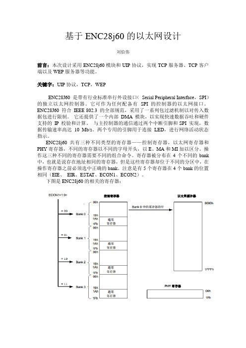
ENC28j60共有三种不同类型的寄存器——控制寄存器,以太网寄存器和PHY寄存器,不同的寄存器以不同的字母开头,以E、MA和MI加以区分。
操作这三种不同的寄存器需要不同的组合命令。
寄存器被分布在4个不同的bank 中,也就是说存在地址相同的寄存器,但是这些寄存器却位于不同的分区中,在操作寄存器之前必须选中正确的bank。
注意是有5个寄存器在4个bank的位置相同(EIE、EIR、ESTAT、ECON1、ECON2)。
下图是ENC28j60的相关的寄存器:ENC28j60的寄存器操作分为2+2+2部分,分别为写寄存器和读寄存器部分,读缓冲区和写缓冲区部分,写PHY寄存器和读PHY寄存器部分。
读写寄存器的分为两步,第一步为选定寄存器的BANK编号,第二步使用写命令或读命令,操作指定地址的寄存。
ENC28j60的应用电路如下图:ENC28J60 由七个主要功能模块组成:1)SPI 接口,充当主控制器和ENC28J60 之间通信通道。
2)控制寄存器,用于控制和监视ENC28J60。
3)双端口RAM 缓冲器,用于接收和发送数据包。
4)判优器,当DMA、发送和接收模块发出请求时对RAM 缓冲器的访问进行控制。

第28卷第3期2007年 6月河南科技大学学报:自然科学版Journal of Henan University of Science and Technol ogy:Natural Science Vol .28No .3Jun .2007基金项目:教育部铁路电力机车牵引及控制项目(V21-W17041)作者简介:张中央(1966-),男,河南孟津人,副教授,从事电力电子技术、电力机车控制、牵引与制动等教学与研究工作.收稿日期:2006-10-13文章编号:1672-6871(2007)03-0049-05基于ENC28J 60的嵌入式系统以太网接口设计张中央,陶乃彬(郑州铁路职业技术学院,河南郑州450052)摘要:介绍了一种基于新型独立以太网控制芯片E NC28J60的以太网通讯接口的软硬件设计方法。
文中详细介绍了新型独立以太网控制器E NC28J60的结构、功能、外围电路以及E NC28J60与C8051F040的SP I 通讯和基于两者的TCP /I P 协议栈的实现的软硬件设计。
E NC28J60以太网控制器采用标准的SP I 串行接口,只需4条连线即可实现与单片机连接,有利于在小型系统上实现以太网功能。
关键词:E NC28J60芯片;以太网;接口;C8051F040;T CP /I P 设计中图分类号:TP393.11文献标识码:A0 前言随着互联网的普及和以太网的迅速发展,基于以太网的设备控制越来越多,发展也越来越快。
目前,以太网已经广泛地应用于各种计算机网络,通过以太网及T CP /I P 协议栈[1]可以使不同的网络控制设备实现互连、交换数据。
用以太网实现嵌入式系统的网络连接有多种方案,传统的多器件以太网连接方案是通过MCU 扩展以太网控制器来实现的,必要时还需要扩展外部RAM 和ROM ,虽然这种方案应用起来不是很困难,但所用外部元件数量较多,系统开销较大,最大的缺点是稳定性不高。
1前言嵌入式以太网开发,可以分为两个部分,一个是以太网收发芯片的使用,一个是嵌入式以太网协议栈的实现。
以太网收发芯片的使用要比串口收发芯片的使用复杂的多,市面上流通比较广泛的以太网收发芯片种类还不少,有SPI接口的ENC28J60,也有并口形式的RTL8019S,CS8900A等。
嵌入式以太网协议栈有著名的uIP协议栈,Lwip协议栈,还有其他嵌入式高手开发的协议栈。
无论是硬件还是软件,都无法分出高低,适合项目需求的才是最好的。
1.1 写作理由再说明一下我写作的理由。
以前从淘宝上购买过ENC28J60,店家信誓旦旦地说能提供51AVR LPC STM32等多个平台的代码,可以实现一个网页控制LED。
头脑一热买了回来,买回来才发现,店家提供的资料零零散散,不易弄懂。
几经周转,发现原来这些ENC28J60的代码都出自一个地方——AVRNET,源自老外的一个开源项目。
把最原始的代码拿来细细品味,以太网协议就不那么神秘了。
在这里说一下ENC28J60的使用,熟悉了ENC28J60的驱动可以分几步走。
第一步,通过ENC28J60移植uIP或者lwIP协议栈,实现TCP或是UDP通信,第二,顺着AVRNET项目走,实现一个简单的web服务器,运行静态或者动态网页。
嵌入式以太网和计算机以太网开发不同,对于TCP通信而言没有socket套接字,对于网页编程而言也没有IIS或PHP,所示实现起来会相对麻烦,但是也非常有乐趣。
1.2 资料准备嵌入式以太网开发是非常复杂的工作,在开始之前最好先大致浏览ENC28J60的使用手册。
除此之外,需要认真阅读TCP IP相关知识,推荐一本图书《嵌入式Internet TCP/IP基础、实现和应用》。
嵌入式开发是一个反复借鉴的过程,该部分代码参考了AVRNET项目和奋斗开发板的相关范例。
【AVRNET项目网址链接】虽然AVRNET项目所使用的MCU为ATmega32,但是认真阅读源代码之后也可以方便的移植到其他的MCU平台,例如STM8、STM32和MSP430等。
ENC28J60的AVR单片机接口设计与网络通信编程作者:黄维铭来源:《数字化用户》2013年第13期本文介绍了带有行业标准串行外设接口(Serial Peripheral Interface,SPI)的独立以太网控制器ENC28J60 在AVR单片机接口开发设计中的应用,以及单片机控制ENC28J60的程序及计算机与ENC28J60进行网络通信的有关程序设计段。
一、概述带SPI接口的ENC28J60由七个主要功能模块组成:1. SPI 接口:充当主控制器和ENC28J60 之间通信通道;2. 控制寄存器:用于控制和监视ENC28J60;3. 双端口RAM缓冲器:用于接收和发送数据包;4. 判优器:当DMA、发送和接收模块发出请求时对RAM 缓冲器的访问进行控制;5. 总线接口:对通过SPI 接收的数据和命令进行解析;6. MAC (Medium Access Control)模块:实现符合IEEE 802.3 标准的MAC 逻辑;7. PHY(物理层)模块——对双绞线上的模拟数据进行编码和译码。
该器件还包括其他支持模块,诸如振荡器、片内稳压器、电平变换器(提供可以接受5V 电压的I/O 引脚)和系统控制逻辑。
二、器件结构接口示意框图ENC28J60 中所有的存储器都是以静态RAM 的方式实现的。
ENC28J60 中有三种类型的存储器:控制寄存器、以太网缓冲器和PHY寄存器,控制寄存器类存储器包含控制寄存器(Control Register,CR)。
它们用于进行ENC28J60 的配置、控制和状态获取。
可以通过SPI 接口直接读写这些控制寄存器。
PHY 寄存器用于进行PHY 模块的配置、控制和状态获取。
PHY 寄存器用于进行PHY 模块的配置、控制和状态获取。
不可以通过SPI 接口直接访问这些寄存器,只可通过MAC 中的MII (Media Independent Interface)访问这些寄存器。
SPI接口以太网控制器ENC28J60及其应用文章发布人:gxy 共36人阅读文字大小:[ 大中小 ] 文字背景色:Ethernet Controller with SPI™ Interface ENC28J60 and Its ApplicationAbstract: Today,most of the Ethernet controller is designed for personal computer, so its applying is much complicated。
The mode of extending bus is often needed. This paper introduces th e world’s smallest package Ethernet controller ENC28J60 at present. Adopting the SPI serial interface mode, so the designing process is predigested. In this paper, it is introduced of the characters, inside structure and PIN function of Ethernet controller ENC28J60. Further more, the paper analyzes the setting of register and process of work in detail and illustrates the application circuit with the interface of MCU.Key Words: Ethernet controller; SPI; ENC28J60摘要:目前大多数以太网控制器都是为个人计算机而设计的,在精简的嵌入式系统中使用比较繁杂,常常需要采用扩展总线的方式,本文介绍了全球目前最小封装的以太网控制器ENC28J60,由于采用SPI串行接口方式,简化了设计,本文介绍了其特性、内部结构和引脚功能,详细分析了其寄存器设置和工作过程,给出了与微控制器接口的应用电路。
关键词:以太网控制器;SPI;ENC28J60一. ENC28J60概述ENC28J60是全球目前最小封装的以太网控制器,在此之前,嵌入式设计人员在为远程控制或监控提供应用接入时可选的以太网控制器都是专为个人计算系统设计的,既复杂、又占空间,且比较昂贵。
目前市场上大部分以太网控制器采用的封装均超过80引脚,而符合IEEE 802.3协议的ENC28J60只有28引脚,就能既提供相应的功能,又可以大大简化相关设计,并减小占板空间。
此外,ENC28J60以太网控制器采用业界标准的SPI™串行接口,只需4条连线即可与主控单片机连接。
这些功能加上由Microchip免费提供的、用于单片机的TCP/IP软件堆栈,使之成为目前市面上最小的嵌入式应用以太网解决方案。
ENC28J60的主要特点如下:兼容的IEEEλ 802.3协议的以太网控制器集成的MAC和10BASE-T物理层λ支持全双工和半双工模式λ数据冲突时可编程自动重发λSPI接口速度高达10Mbpsλ8K数据接收发送双端口RAMλ提供快速数据移动的内部DMA控制器λ可配置的接收发送缓冲区大小λ支持单播、多播和广播λ两个可编程LED输出λ带7个中断源的两个中断引脚λTTL电平输入λ二. ENC28J60的内部结构及其引脚功能ENC28J60采用28引脚封装,内部接口引脚如图1,ENC28J60兼容IEEE 802.3协议,内部集成了物理层,支持全双工和半双工模式,芯片内的8K双端口RAM可以自由进行配置,特殊的过滤器,包括Microchip的可编程模式匹配过滤器,可自动评价、接受或拒收Magic Packet™、单播(Unicast)、多播(Multicast)或广播(Broadcast)信息包,以减轻主控单片机的处理负荷。
各个引脚功能如下:ENC28J60引脚简单,SPI接口和单片机相连接,网络的四个引脚通过网络变压器后连接到RJ45接口,两个中断引脚接单片机的外部中断或者连接到通用IO口,两个指示灯引脚外接发光管连接到地或者电源,其余引脚是电源和地。
ENC28J60内部采用3.3V电源,但是其接口都可以容忍5V的电压值,在使用3.3V电源的单片机系统中,可以直接将SPI接口和中断连接到单片机,如果使用5V的单片机,ENC28J60的输入引脚直接连接到单片机,输出引脚需要外接一个与门或者三态门进行5V的驱动。
振荡器可以选用无源晶体或者有源晶振。
三. ENC28J60的寄存器设置和工作过程ENC28J60内部的静态RAM分为三种类型,控制寄存器,以太网缓冲区和物理层寄存器,控制寄存器用来进行芯片的配置和控制等功能,直接SPI读写;以太网缓冲区可以由SPI 接口配置为接收和发送以太网数据包的RAM区;物理层寄存器用来配置,控制和监测物理层的状态,此寄存器不能直接由SPI接口读写,只能通过媒体独立接口MII访问。
ENC28J60控制寄存器中最基本和重要的5个寄存器是EIE, EIR, ESTAT, ECON2 和ECON1,其功能分别如下,EIE:以太网中断使能控制寄存器,分为总中断使能和各部分使能控制,EIR:以太网中断标志寄存器,在接收和发送数据包时根据不同的标志位进入不同的执行程序,ESTAT:以太网状态寄存器,反映以太网当前是否数据碰撞、忙信息、错误信息、时钟状态等信息,ECON2:以太网辅助控制寄存器,设置数据指针,芯片节能等,ECON1:以太网主控制寄存器,这个是芯片最常用的寄存器,主要用来设置不同层的寄存器空间,下面将详细论述。
在这5个寄存器中,需要设置的是EIE、ECON2和ECON1,需要判断标志位的是EIR和ESTAT。
ENC28J60的控制寄存器分为4层,由ECON1寄存器中的最后两位BSEL1:BSEL0进行设置,每一层包含32个控制寄存器,最后5个寄存器地址映射的位置一样,即为上述的5个基本寄存器,0层寄存器包括设置发送缓冲区起始地址ETXST和结束地址ETXND,接收缓冲区起始ERXST和结束地址ERXND,数据指针的初始化位置EWRPT和ERDPT,DMA 控制等。
1层寄存器设置包括数据过滤用的64位的hash表,数据过滤用的EPM,网络中断唤醒使能位EWOLI,接收滤波控制ERXFCON,以太网数据包计数EPKTCNT,2层寄存器设置包括MAC配置MACCON、数据冲突MACLCON、最大帧长MAMXFL、MII寄存器等,3层寄存器设置包括MAC地址MACADR、自检EBST、MII状态MISTAT、以太网版本信息EREVID、时钟输出控制ECOCON、以太网流控制EFLOCON、暂停时间值EPAUSL。
以太网缓冲区大小共8K字节,可以通过SPI接口编程配置成接收和发送缓冲区两大部分,由以太网控制器相关寄存器进行设置。
物理层寄存器共有32个寄存器,其中只有9个可以使用,每个寄存器为16位宽度,不能直接由SPI总线读写,主要配置的寄存器包括物理层的复位、节电、双工设置,LED的设置等,读取的方法为先将需要读取的物理层地址写入MIREGADR,设置MICMD.MIIRD位,延时后判断MISTAT.BUSY是否被自动清除,然后清除MICMD.MIIRD,从MIRDL 和MIRDH中读取数据,写物理层寄存器要求一次写入16位,先将需要写的物理层地址写入MIREGADR,然后写低8位到MIWRL,高8位到MIWRH,写入数据期间MISTAT.BUSY 自动置位,写入结束后该位自动清除。
在ENC28J60接收和发送数据包之前,需要对相应寄存器进行设置和初始化,一般情况下这部分工作放在系统复位完成后执行,初始化设置工作包括接收和发送缓冲区、接收过滤、晶振启动时间、MAC寄存器、物理层。
初始化芯片之前先关闭单片机的中断输入,对RESET 引脚给定一个持续的低电平复位信号,然后对相应的寄存器进行设置。
设置完成所有需要的寄存器后,判断以太网状态中的时钟启动标志位是否置位,然后开中断,以上的流程图如2所示。
硬件连接的两个中断引脚都对应多种中断条件,EIE和EWOLIE分别使能不同的中断,均指向中断入口处,因此需要在入口处进行判断每次的中断输入什么条件,EIR是中断标志位,包含了7中不同的中断条件,根据不同的标志位进入不同的执行程序。
图2 主程序初始化流程图四. ENC28J60的应用由于采用串行SPI接口,ENC28J60可以很方便地和各种微控制器和处理器接口,构成嵌入式以太网模块,使用UDP,TCP进行通信,或者构建嵌入式WEB服务器,对于没有SPI 接口的微控制器,也可以用通用IO模拟SPI总线的方法,下图是一个51内核单片机C8051F133和ENC28J60的接口,C8051F133采用3.3V供电,70%的指令的执行时间为一个或两个系统时钟周期,内部8k字节内部数据RAM,64K程序FLASH,速度可达100MIPS,与ENC28J60可构成最佳以太网应用。
C8051F133的SPI接口SCK、MISO、MOSI分别连接ENC28J60的SCK、SI、SO引脚,C8051F133的两个外部中断输入引脚连接ENC28J60的INT和WOL,系统中还有一片X5043用于看门狗,复位和保存以太网参数。
五.结论由ENC28J60构成的嵌入式以太网模块电路连接简单,功能强大,与目前大多数需要并行数据和地址总线的以太网控制器相比,不需要小封装的微控制器外扩地址和数据总线,有很大优点,根据需要配合不同的微控制器可以将电路板做到最小尺寸,完全符合未来工业以太网控制器的发展趋势,本文中的应用电路已经应用于嵌入式控制系统,目前仍在稳定运行中。
文章的主要创新之处如下:1. 首次应用ENC28J60构成嵌入式以太网模块电路。
2. 克服了市场上已有以太网控制器封装引脚多的缺点,简化了设计,减小了占板空间。
ENC28J60以太网控制器采用标准的SPI串行接口,只需4条连线与主控单片机相连。
参考文献:[1] ENC28J60 Stand-Alone Ethernet Controller with SPI 2004 Microchip TechnologyInc. Interface[2] 陈奎吴爱国游洲用ENC28J60和FPGA设计通用以太网控制器电子产品世界2005.11 94页-95页[3] 林安兵.使用华恒HHARM4510-R2进行嵌入式开发[J],微计算机信息,2005.21(2):113-115[4] 郁继宗, 彭树生.基于PIC单片机的以太网数据采集与控制电路设计,微计算机信息,2005,21(2):72-74作者简介:祁树胜(1965.4-),男,1985年毕业于天津大学自动化工程系,工学学士,1985年以来在西安航空技术高等专科学校从事教学及智能仪表,计算机测控等科研工作。