NXP ARM MCU Introduction - Cortex Core - 20100113_R
- 格式:pdf
- 大小:1.26 MB
- 文档页数:62
手机CPU处理器架构进化历程随着智能手机越来越普及,消费者在选购手机的时候也越来越理性化,除了关心价格和外观之外,手机的性能也成为了人们最关心的因素,大家都知道,处理器是影响手机性能的最关键的因素,像德州仪器、高通、英伟达以及三星等主流的处理器厂商,大家都已经耳熟能详。
但是很多人并不知道,其实它们采用的都是同一个架构——ARM架构,实际上,处理器采用的架构才是影响处理器性能的关键因素。
今天,笔者就和大家一起,聊一聊ARM的那些事。
ARM架构简介ARM架构简介ARM(Advanced RISC Machine的缩写)架构,被称作进阶精简指令集机器,是一个32位精简指令集(RISC)处理器架构,其广泛地使用在许多嵌入式系统设计。
由于低成本、高效能、低耗电的特性,ARM处理器非常适用于移动通讯领域。
为了大家更好的理解,我们不妨做个比喻,ARM架构就像是一座建筑的结构设计部分,而处理器就相当于一个完整的建筑,只有有了稳定的结构作为基础,才能建造出各式各样的房子。
换句话说,ARM架构只相当于一座建筑的框架,至于最后建造出来的房子长什么样,舒适度如何,就是由处理器厂商自己决定了。
不过有一点需要说明,假如结构的设计值是十层,容纳人数的上限是100人,那么最后建好的房子也不能超过这个上限。
这也就是说,采用相同架构的处理器,性能基本上已经锁定在一定的范围之内,不会有本质的区别。
所以,看处理器的性能要先看架构。
ARM架构ARM授权方式ARM公司是一家知识产权供应商,本身并不参与终端处理器芯片的制造和销售,而是通过向其它芯片厂商授权设计方案,来获取收益。
ARM提供了多样的授权方式,ARM公司可以向芯片厂商单纯的转让设计方案的使用及销售权,比如德州仪器,其旗下的OMAP处理器是在原始ARM架构的基础上设计的,这种方式费用一般比较低,所以,德州仪器的芯片售价也相对较低。
对于一些具备自有设计技术的客户,他们希望能对原始的ARM架构进行优化,以便更好的适应到自己研发的芯片,这样就会牵扯到授权架构修改的费用,而且这项费用也是相当昂贵的。

Cortex—M系列M0:Cortex—M0是目前最小的ARM处理器,该处理器的芯片面积非常小,能耗极低,且编程所需的代码占用量很少,这就使得开发人员可以直接跳过16位系统,以接近8 位系统的成本开销获取32 位系统的性能。
Cortex—M0 处理器超低的门数开销,使得它可以用在仿真和数模混合设备中。
M0+:以Cortex-M0 处理器为基础,保留了全部指令集和数据兼容性,同时进一步降低了能耗,提高了性能.2级流水线,性能效率可达1。
08 DMIPS/MHz。
M1:第一个专为FPGA 中的实现设计的ARM 处理器。
Cortex—M1 处理器面向所有主要FPGA 设备并包括对领先的FPGA 综合工具的支持,允许设计者为每个项目选择最佳实现.M3:适用于具有较高确定性的实时应用,它经过专门开发,可使合作伙伴针对广泛的设备(包括微控制器、汽车车身系统、工业控制系统以及无线网络和传感器)开发高性能低成本平台。
此处理器具有出色的计算性能以及对事件的优异系统响应能力,同时可应实际中对低动态和静态功率需求的挑战。
M4:由ARM 专门开发的最新嵌入式处理器,用以满足需要有效且易于使用的控制和信号处理功能混合的数字信号控制市场。
M7:在ARM Cortex—M 处理器系列中,Cortex—M7 的性能最为出色。
它拥有六级超标量流水线、灵活的系统和内存接口(包括AXI 和AHB)、缓存(Cache)以及高度耦合内存(TCM),为MCU 提供出色的整数、浮点和DSP 性能.互联:64位AMBA4 AXI, AHB外设端口(64MB 到512MB)指令缓存:0 到64kB,双路组相联,带有可选ECC数据缓存:0 到64kB,四路组相联,带有可选ECC指令TCM:0 到16MB,带有可选ECC数据TCM:0 到16MB,带有可选ECCCortex-A系列:ARM Cortex—A 系列是一系列用于复杂操作系统和用户应用程序的应用程序处理器。
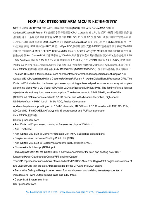
NXP i.MX RT500双核ARM MCU嵌入应用开发方案NXP公司的i.MX RT500是嵌入应用的双核微控制器(MCU),包括Arm Cortex-M33 CPU和CadenceRXtensaR Fusion F1音频数字信号处理器CPU. Cortex-M33 CPU包括两个硬件协处理器,提供增强性能,用于一系列复杂算法和带有LCD接口和MIPI DSI PHY的2D失量GPU.该系列具有丰富的外设和非常低的功耗.器件有多达5MB SRAM,两个FlexSPIs (Octal/Quad SPI 接口),每个有32KB缓存,以及一个动态加密,高速USB器件/主+PHY,12位1MSps ADC,模拟比较器,支持8 DMIC通路的音频子系统,2D GPU 和LCD控制器以及MIPI DSI PHY, SDIO/eMMC; FlexIO; AES/SHA/Crypto M33协处理器和PUF键发生器.控制处理器Arm Cortex-M33工作频率高达200MHz,并内置了嵌套中断向量控制器(NVIC),主外接电源1.8V ± 5%, Vddcore电源从0.6V到1.1V可调,模拟电源1.71-3.6 V,五个VDDIO电源为1.71 - 3.6 V,USB电源为3.0-3.6 V.主要用在工业领域,智能可穿戴市场以及,智能家庭,物联网(IOT)和玩具与棋类游戏.本文介绍了i.MX RT500主要特性,框图和评估板i.MX RT500 EVK (MIMXRT595-EVK) 技术和功能指标以及电路图. The i.MX RT500 is a family of dual-core microcontrollers forembedded applications featuring an Arm Cortex-M33 CPUcombined with a CadenceRXtensaR Fusion F1 Audio DigitalSignal Processor CPU. The Cortex-M33 includes two hardwarecoprocessors providing enhanced performance for an array ofcomplex algorithms along with a 2D Vector GPU with LCDInterface and MIPI DSI PHY. The family offers a rich set ofperipherals and very low power consumption. The device has upto 5 MB SRAM, two FlexSPIs(Octal/Quad SPI Interfaces) eachwith 32 KB cache, one with dynamic decryption, high-speed USBdevice/host + PHY, 12-bit 1 MS/s ADC, Analog Comparator,Audio subsystems supporting up to 8 DMIC channels, 2D GPUand LCD Controller with MIPI DSI PHY, SDIO/eMMC; FlexIO;AES/SHA/Crypto M33 coprocessor and PUF key generationi.MX RT500主要特性:Control processor core• Arm Cortex-M33 processor, running at frequencies ofup to 200 MHz• Arm TrustZone• Arm Cortex-M33 built-in Memory Protection Unit (MPU)supporting eight regions• Single-precision Hardware Floating Point Unit (FPU).• Arm Cortex-M33 built-in Nested Vectored InterruptController (NVIC).• Non-maskable Interrupt (NMI) input.• Two coprocessors for the Cortex-M33: a hardwareaccelerator for fixed and floating point DSP functions(PowerQuad) and a Crypto/FFT engine (Casper).TheDSP coprocessor uses a bank of four dedicated 2 KBSRAMs. The Crypto/FFT engine uses a bank of two 2KB SRAMs that are also AHB accessible by the CPUand the DMA engine.• Serial Wire Debug with eight break points, four watchpoints, and a debug timestamp counter. It includesSerial Wire Output (SWO) trace and ETM trace.• Cortex-M33 System tick timerDSP processor core• Cadence Tensilica Fusion F1 DSP processor, runningat frequencies of up to 200 MHz.• Hardware Floating Point Unit.• Serial Wire Debug (shared with Cortex-M33 ControlDomain CPU).Communication interface• 9 configurable universal serial interface modules(Flexcomm Interfaces). Each module contains anintegrated FIFO and DMA support. Each of the ninemodules can be configured as:• A U SART with dedicated fractional baud rategeneration and flow-control handshakingsignals. The USART can optionally be clockedat 32 kHz and operated when the chip is inreduced power mode, using either the 32 kHzclock or an externally supplied clock. TheUSART also provides partial support forLIN2.2.• An I2C-bus interface with multiple addressrecognition, and a monitor mode. It supports400 Kb/sec Fast-mode and 1 Mb/sec FastmodePlus. It also supports 3.4 Mb/sec highspeedwhen operating in slave mode.• An SPI interface.• An I2S (Inter-IC Sound) interface for digitalaudio input or output. Each I2S supports up tofourchannel-pairs.• Two additional high-speed SPI interfaces supporting50 MHz operation• One additional I2C interface with open-drain pads• Two I3C bus interfaces• A digital microphone interface supporting up to 8channels with associated decimators and VoiceFive I/O Power Rails• Five independent supplies powering different clustersof pins to permit interfacing directly tooff-chipperipherals operating at different supply levels.On-chip memory• Up to 5 MB of system SRAM accessible by both CPUs,both DMA engines, the Graphics Subsystem and allother AHB masters.• Additional SRAMs for USB traffic (16 KB), Cortex-M33co-processors (4 x 2 KB), SDIO FIFOs (2 x 512 B dualport),PUF secure key generation (2 KB), FlexSPIcaches (32 KB each), SmartDMA commands (32 KB),and a variety of dual and single port RAMs forgraphics.• 16 kbits OTP fuses• Up to 192 KB ROM memory for factory-programmeddrivers and APIs• System boot from High-speed SPI, FlexSPI Flash, HSUSB, I2C, UART or eMMC via on-chip bootloadersoftware included in ROM. FlexSPI boot mode willinclude an option for Execute-in-placestart-up for nonsecureboot.Digital peripherals• Two general purpose DMA engines, each with 37channels and up to 27 programmablerequest/triggersources.• Can be configured such that one DMA is secureand the other non-secure and/or one can bedesignated for use by the M33 CPU and theother by the DSP• Smart DMA Controller with d edicated 32KB code RAM• USB high-speed host/device controller with on-chipPHY and dedicated DMA controller.• Two FlexSPI (Octal/Quad) Interfaces up to 200 MHzDDR/SDR (target). 32 KB caches with selectablecache policies based on programmable addressregions. One of the FlexSPI interface will include onthe-fly decryption for execute-in-place and addressremappingto support dual-image boot. DMA supported(both modules).• Two SD/eMMC memory card interfaces with dedicatedDMA controllers. One supports eMMC 5.0 withHS400/DDR operation.Analog peripherals• One 12-bit ADC with sampling rates of 1 Msamples/secand an enhanced ADC controller. It supports up to 10single-ended channels or 5 differential channels. TheADC supports DMA.• Temperature sensor.• Analog compar atorActivation Detect. One pair of channels can bestreamed directly to I2S. The DMIC supports DMA.Timers• One 32-bit SCTimer/PWM module (SCT). Multipurposetimer with extensiveevent-generation,match/compare, and complex PWM and outputcontrol features.• 10 general-purpose/PWM outputs, 8 generalpurposeinputs• It supports DMA and can trigger external DMAevents• It supports fractional match values for highresolution• Five general purpose, 32-bit timer/counter moduleswith PWM capability• 24-bit multi-rate timer module with 4 channels eachcapable of generating repetitive interrupts atdifferent, programmable frequencies.• Two Windowed Watchdog Timers (WDT) withdedicated watchdog oscillator (1 MHz LPOSC)• Frequency measurement module to determine thefrequen cy of a selection of on-chip or off-chip clocksources.• Real-Time Clock (RTC) with independent powersupply and dedicated oscillator. Integratedwake-uptimer can be used to wake the device up from lowpowermodes. The RTC resides in the “always-on”voltage do main. RTC includes eight 32-bit generalpurposeregisters which can retain contents whenpower is removed from the rest of the chip.• Ultra-low power micro-tick Timer running from theWatchdog oscillator with capture capability fortimestamping. Can be used to wake up the devicefrom low-power modes.• 64-bit OS/Event Timer common to both processorswith individual match/capture and interruptgeneration logic. Enabled on PORClocks• Crystal oscillator with an operating range of 4 MHzto 26 MHz.• Dual trim option: Internal 192/96 MHz FROoscillator. Trimmed to 1% accuracy.• FRO capable of being tuned using an accuratereference clock (eg. XTAL Osc) to 0.1% accuracywith 46% duty cycle to support MIPI PHY andFlexSPI.• Internal 1 MHz low-power oscillator with 5%accuracy. Serves as the watchdog oscillator andclock for the OS/Event Timer and the Systick amongothers.Also available as the system clock to bothdomains.• 32 kHz real-time clock (RTC) oscillator that canoptionally be used as a system clock.• Main Syste m PLL:• allows CPU operation up to the maximum ratewithout the need for a high-frequency crystal.Graphics/Multimedia• 2D Vector Graphics Processing Unit, running atfrequencies of up to 200 MHz.• LCD Display Interface supporting smart LCD displaysand vi deo mode.• MIPI DSI Interface with on-chip PHY supportingtransfer rates up to 895.1 Mbps.• FlexIO can be configured to provide a parallel interfaceto an LCDI/O Peripherals• Up to 136 general purpose I/O (GPIO) pins withconfigurable pull-up/pull-down resistors. Ports can bewritten as words, half-words, bytes, or bits.• Mirrored, secure GPIO0.• Individual GPIO pins can be used as edge and levelsensitive interrupt sources, each with its own interruptvector.• All GPIO pins can contribute to one of two ganged(OR’d) interrupts from the GPIO_HS module.• A group of up to 7 GPIO pins (from Port0/1) can beselected for Boolean pattern matching which cangenerate interrupts and/or drive a “pattern-match”output.• Adjustable output driver slew rates.• JTAG bounda ry scanSecurity• Secure Isolation: Protection from software and remoteattacks using Trustzone for armV8M. Hardwareisolation of AES keys• Secure Boot: firmware in ROM providing immutableroot of trust• Secure Storage: Physically Unclonable Function(PUF) based key store, On-the-fly-AESdecryption(OTFAD) of off-chip flash for code storage• Secure Debug: Certificate based debug authenticationmechanism• Secure Loader: Supports firmware update mechanismwith authenticity (RSA signed) and confidentiality(AES-CTR encrypted) protection• Secure Identity: 128-bit Universal Unique Identifier(UUID), 256-bit Compound Device Identifier (CDI) perTCG DICE specification• Cryptographic Accelerators• Symmetric cryptography (AES) with128/192/256-bit key strength and protectionagainst Side-channel analysis (Differential PowerAnalysis and Template attacks)• Asymmetric cryptography acceleration usingCASPER co-processor• NIST SP 800-90b compliant TRNG design with512-bit output per call• Hash engine with SHA-256 and SHA1May be run from the FRO, the crystaloscillator or the CLKIN pin. • a second, independent PLL output providesalternate high-frequency clock source for theDSP CPU if the required frequency is differentfrom the main system clock. (Note: 2nd PFDoutput from Main System PLL) • two additional PLL outputs provide potentialclock sources to various peripherals.• Audio PLL for the audio subsystem.Power Control• Main external power supply: 1.8V ± 5%• Vddcore supply (from PMIC or internal PMU):adjustable from 0.6 V to 1.1 V (including retentionmode) • Analog supply: 1.71-3.6 V• Five VDDIO supplies (can be shared orindependent): 1.71 - 3.6 V• USB Supply: 3.0-3.6 V• Reduced power modes:• Sleep mode: CPU clock shut down (each CPUindependently)• Deep_sleep mode: Us er-selectableconfiguration via PDSLEEPCFG• Deep_powerdown mode: Internal powerremoved from entire chip except “always-on”domain• Each individual SRAM partition can beindependently powered-off or put into a lowpowerretain mode• DSP Domain can be powered-offindependently from the rest of the system.• Ability to operate the synchronous serialinterfaces in sleep or deep-sleep as a slave orUSART clocked by the 32 kHz RTC oscillator• Wake-up from low-power modes via interruptsfrom various peripherals including the RTCand the OS/Event timer• RBB/FBB to provide additional control over power/performance trade-offs• Power-On Reset (POR).Operating characteristics• Temperature range (ambient): -20 °C to +70 °C• VDDCORE: 0.7 V - 1.155 V• VDDIO_0/1/2/4: 1.71 V - 1.89 V• VDDIO_3: 1.71 V - 3.6 V图2.评估板i.MX RT500 EVK (MIMXRT595-EVK)外形图(正面)图3.评估板i.MX RT500 EVK (MIMXRT595-EVK)外形图(背面)图4.评估板i.MX RT500 EVK (MIMXRT595-EVK)电路图(1)图5.评估板i.MX RT500 EVK (MIMXRT595-EVK)电路图(2)图6.评估板i.MX RT500 EVK (MIMXRT595-EVK)电路图(3)图7.评估板i.MX RT500 EVK (MIMXRT595-EVK)电路图(4)图8.评估板i.MX RT500 EVK (MIMXRT595-EVK)电路图(5)图9.评估板i.MX RT500 EVK (MIMXRT595-EVK)电路图(6)图10.评估板i.MX RT500 EVK (MIMXRT595-EVK)电路图(7)图11.评估板i.MX RT500 EVK (MIMXRT595-EVK)电路图(8)图12.评估板i.MX RT500 EVK (MIMXRT595-EVK)电路图(9)图13.评估板i.MX RT500 EVK (MIMXRT595-EVK)电路图(10)图14.评估板i.MX RT500 EVK (MIMXRT595-EVK)电路图(11)图15.评估板i.MX RT500 EVK (MIMXRT595-EVK)电路图(12)图16.评估板i.MX RT500 EVK (MIMXRT595-EVK)电路图(13)图17.评估板i.MX RT500 EVK (MIMXRT595-EVK)电路图(14)图18.评估板i.MX RT500 EVK (MIMXRT595-EVK)电路图(15)图19.评估板i.MX RT500 EVK (MIMXRT595-EVK)电路图(16)图20.评估板i.MX RT500 EVK (MIMXRT595-EVK)电路图(17)图21.评估板i.MX RT500 EVK (MIMXRT595-EVK)电路图(18)。

什么是MCU?MCU基础知识讲解诸多原因显示,MCU在2018年将继续缺货。
1、汽车电子及物联网大量导入MCU架构,需求爆发2、ST、TI、瑞萨等IDM厂产能不足,导致交期拉长。
据悉,不少MCU厂商产品交期都从4个月延长至6个月,日本MCU厂商更是拉长至9个月。
3、原材料的上涨。
目前已经有晶圆厂宣布涨价,可能会对MCU造成涨价缺货。
什么是MCU?MCU,中文简称单片机。
即将CPU、存储器(RAM和ROM)、多种I/O接口等集成在一片芯片上,形成的芯片级计算机。
CPU:包括运算器、控制器和寄存器组。
是MCU内部的核心部件,由运算部件和控制部件两大部分组成。
前者能完成数据的算术逻辑运算、位变量处理和数据传送操作,后者是按一定时序协调工作,是分析和执行指令的部件。
存储器:包括ROM和RAM。
ROM程序存储器,MCU的工作是按事先编制好的程序一条条循序执行的,ROM程序存储器即用来存放已编的程序(系统程序由制造厂家编制和写入)。
存储数据掉电后不消失。
ROM又分为片内存储器和片外(扩展)存储器两种。
RAM数据存储器,在程序运行过程中可以随时写入数据,又可以随时读出数据。
存储数据在掉电后不能保持。
RAM也分为片内数据存储器和片外(扩展)存储器两种。
I/O接口:与外部输入、输出(电路)设备相连接。
PO/P1/P2/P3等数字I/O接口,内部电路含端口锁存器、输出驱动器和输入缓冲器等电路。
4位、8位、16位、32位、64位MCU的用途4位计算器、车用仪表、车用防盗装置、呼叫器、无线电话、CD播放器、LCD驱动控制。
微软全新Surface Pro拆解:SSD焊死拆机不可取易报废今年 5 月底,微软为了表示对中国客户的诚意,特别在上海召开了一场新品发布会。
在这波新品当中,最受瞩目的自然是全新 Surface Pro。
这是微软全新一代 Surface Pro 产品,不过并没有以 Surface Pro 5 命名。
不过,在该设备身上还是有诸多全新的亮点,例如 Surface 产品线中最出色的显示屏幕,还有可以变身成“创意画板”的 165 度新铰链设计等。
当然了,全新 Surface Pro 的内部已经升级到了英特尔第七代 Kaby Lake 微架构的酷睿处理器,其中内置酷睿 m3 处理器和 i5 处理器的版本可实现了“无风扇设计”,因此全新 Surface Pro 也成为了全球首款无风扇设计的内置 i5 处理器的设备。
微软还认为,得益于内部的改进,Surface Pro 5 成为了有史以来最轻便的 Surface 设备。
那么全新 Surface Pro 内部到底改进了些什么呢?唯有拆解方知!最近,知名拆解网站 iFixit 正好拆解了全新的 Surface Pro 5,我们来一探究竟。
iFixit 称,从外形表面上来看,全新 Surface Pro 看起来与去年的 Surface Pro 4 非常的相似,但内部规格和设计肯定有所不同。
在拆解之前,先来了解全新 Surface Pro 的一些公布的主要硬件,如下:- 12.3 英寸 PixelSense 显示屏,IPS 面板,分辨率为 2736 x 1824 (267 PPI)像素,3:2 屏幕比例,支持 10 点多点触控。
- 英特尔 Kaby Lake 架构处理器,最低 Core M3(4M 缓存、2.7GHz),最高 Core i7 (4M缓存、4.0GHz)- 4GB/8GB/16GB 三档容量的 1600MHz DDR3L 内存- 128GB/256GB/512GB/1TB 高速固态硬盘- 800 万像素自动对焦后置摄像头,500 万像素前置摄像头- 1 个全尺寸 USB 3.0 接口、microSDXC 读卡器、Surface Connect 接口、3.5mm 耳机插孔、。
基于ARM处理器的微控制器内存问题闪存现在完全主导着微控制器(MCU),但随着处理器升级到32位架构并且外设变得更加强大,存储器考虑变得更加复杂。
很容易忘记外设中的内存,这些外设使MCU更像是一个包含高级电机控制、图形用户界面(GU1)和网络的片上系统(SOC)。
尽管如此,F1ash和其他存储器类型的细节仍值得关注,以确保所选MCU具有符合系统需求的存储器。
在MCU中以更高速度快速使用ARM®Cortex w-M处理器架构也需要更仔细地检查内存支持。
供应商对其片上存储器选项采取不同的方法,这可能会影响选择哪个MCU的平衡。
如今,在更大的MCU上可以使用多达1兆字节的闪存。
随着MCU发现新应用并具有新功能,程序存储、数据表和暂存器RAM的比例发生了变化。
高端MeU可能使用高级语言(H11)进行编程,运行实时操作系统(皿),并使用现成的堆栈和软件包。
这些因素中的每一个都会影响内存需求和使用。
通常用于MCU的闪存的访问时间可以跟上25到50MHz的处理器时钟。
当高性能处理器内核的时钟频率超过200MHz时,可能会有一个巨大的差距来填补耗时耗电的等待状态。
多个片上总线和特殊的路由机制对于缓解一些繁忙的微控制器中的流量问题非常有益。
ARM处理器内核架构由于其紧凑的ThUn1b2®指令而具有非常好的代码密度,该指令仅需要16位来存储指令,而不是预期的32位。
ARMCorteχ-M0>Corteχ-M3和Corteχ-M4内核在众多供应商的微控制器中都很流行,这里将研究一些内存选择。
NXP Semiconductors1PC4000-实时辅助数据处理NXPSemiconductors自从很久以前将ARM7TDMI®内核用于MCU以来,它就在基于ARM的微控制器上取得了成功。
恩智浦在Cortex-M内核推出后迅速将其添加到其产品组合中,并且一直是将CorteX-M3、Cortex-MO和Cortex-M4集成到一端高速的MCU中的领导者之一,同时将价格推低至另一个。
常用的单片机品牌和型号介绍单片机(Microcontroller)是一种集成了微处理器核心、存储器和各种外设接口的集成电路,广泛应用于嵌入式系统中。
单片机能够完成各种控制和计算任务,因此在电子领域中使用非常广泛。
本文将介绍几个常用的单片机品牌和型号,以帮助读者选择适合自己项目的单片机。
一、STMicroelectronicsSTMicroelectronics(意法半导体)是全球领先的半导体供应商之一,提供多种单片机产品。
其中,STM32系列是STMicroelectronics最为著名的单片机系列之一,基于ARM Cortex-M内核。
STM32系列广泛应用于各种嵌入式设备,具有高性能、低功耗等特点。
常见的型号包括STM32F0、STM32F1、STM32F4等,适用于不同的应用场景。
二、AtmelAtmel是一家美国公司,也是全球最大的单片机供应商之一。
Atmel的AVR系列单片机以其高性能和易用性而闻名。
AVR系列单片机具有低功耗、快速执行速度和丰富的外设接口,非常适合于各种嵌入式应用。
其中,ATmega328P是最常用的型号之一,广泛使用于Arduino开发板等项目中。
三、Texas InstrumentsTexas Instruments(德州仪器)是一家世界领先的半导体公司,提供多种单片机产品。
MSP430系列是Texas Instruments的一系列低功耗、高集成度的单片机产品,适用于各种便携式设备和电池供电系统。
MSP430系列单片机具有强大的外设功能和丰富的存储器选项,常见的型号有MSP430G2553、MSP430F5529等。
四、MicrochipMicrochip是一家专注于微控制器和模拟半导体的供应商,其PIC 单片机系列非常知名。
PIC系列单片机具有低功耗、高稳定性和广泛的外设接口,适用于各种应用场景。
其中,PIC16F877A是最常用的型号之一,常见于工业自动化、家电控制等领域。
Cortex-M系列M0:Cortex-M0是目前最小的ARM处理器,该处理器的芯片面积非常小,能耗极低,且编程所需的代码占用量很少,这就使得开发人员可以直接跳过16位系统,以接近8 位系统的成本开销获取 32 位系统的性能。
Cortex-M0 处理器超低的门数开销,使得它可以用在仿真和数模混合设备中。
M0+:以Cortex-M0 处理器为基础,保留了全部指令集和数据兼容性,同时进一步降低了能耗,提高了性能。
2级流水线,性能效率可达1.08 DMIPS/MHz。
M1:第一个专为 FPGA 中的实现设计的 ARM 处理器。
Cortex-M1 处理器面向所有主要 FPGA 设备并包括对领先的 FPGA 综合工具的支持,允许设计者为每个项目选择最佳实现。
M3:适用于具有较高确定性的实时应用,它经过专门开发,可使合作伙伴针对广泛的设备(包括微控制器、汽车车身系统、工业控制系统以及无线网络和传感器)开发高性能低成本平台。
此处理器具有出色的计算性能以及对事件的优异系统响应能力,同时可应实际中对低动态和静态功率需求的挑战。
M4:由 ARM 专门开发的最新嵌入式处理器,用以满足需要有效且易于使用的控制和信号处理功能混合的数字信号控制市场。
M7:在 ARM Cortex-M 处理器系列中,Cortex-M7 的性能最为出色。
它拥有六级超标量流水线、灵活的系统和存接口(包括 AXI 和 AHB)、缓存(Cache)以及高度耦合存(TCM),为MCU 提供出色的整数、浮点和 DSP 性能。
互联:64位 AMBA4 AXI, AHB外设端口 (64MB 到 512MB)指令缓存:0 到 64kB,双路组相联,带有可选 ECC数据缓存:0 到 64kB,四路组相联,带有可选 ECC指令TCM:0 到 16MB,带有可选 ECC数据TCM:0 到 16MB,带有可选 ECCCortex-M系列规格对比Cortex-A系列:ARM Cortex-A 系列是一系列用于复杂操作系统和用户应用程序的应用程序处理器。