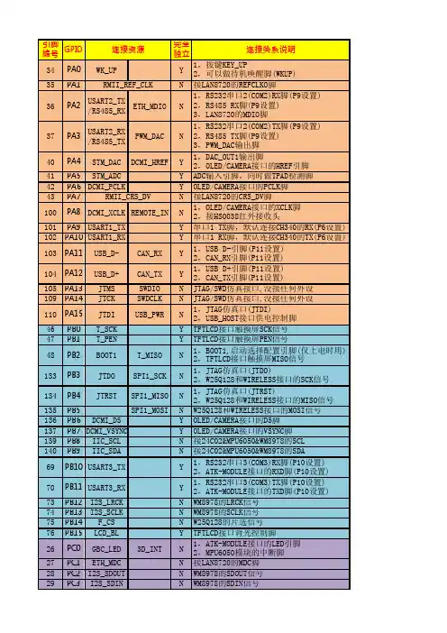
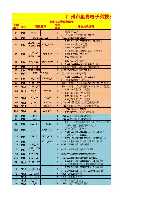
STM32_引脚排列xls格式
- 格式:xls
- 大小:46.50 KB
- 文档页数:16

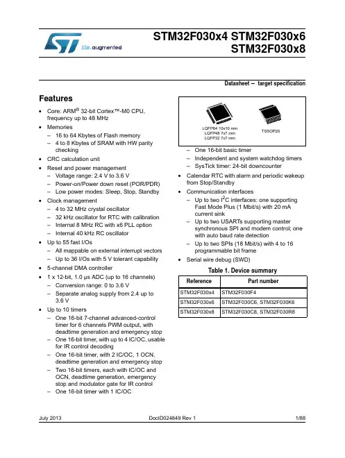
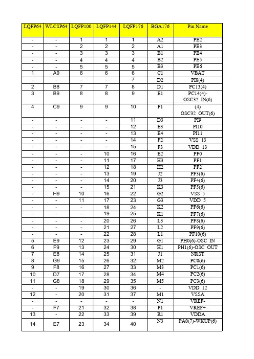
Contents STM32F103x8,STM32F103xB Contents1Introduction (9)2Description (9)2.1Device overview (10)2.2Full compatibility throughout the family (13)2.3Overview (14)2.3.1ARM®Cortex™-M3core with embedded Flash and SRAM (14)2.3.2Embedded Flash memory (14)2.3.3CRC(cyclic redundancy check)calculation unit (14)2.3.4Embedded SRAM (14)2.3.5Nested vectored interrupt controller(NVIC) (14)2.3.6External interrupt/event controller(EXTI) (15)2.3.7Clocks and startup (15)2.3.8Boot modes (15)2.3.9Power supply schemes (15)2.3.10Power supply supervisor (15)2.3.11Voltage regulator (16)2.3.12Low-power modes (16)2.3.13DMA (17)2.3.14RTC(real-time clock)and backup registers (17)2.3.15Timers and watchdogs (17)2.3.16I²C bus (19)2.3.17Universal synchronous/asynchronous receiver transmitter(USART)..192.3.18Serial peripheral interface(SPI) (19)2.3.19Controller area network(CAN) (19)2.3.20Universal serial bus(USB) (19)2.3.21GPIOs(general-purpose inputs/outputs) (20)2.3.22ADC(analog-to-digital converter) (20)2.3.23T emperature sensor (20)2.3.24Serial wire JTAG debug port(SWJ-DP) (20)3Pinouts and pin description (21)4Memory mapping (34)2/105DocID13587Rev16STM32F103x8,STM32F103xB Contents5Electrical characteristics (35)5.1Parameter conditions (35)5.1.1Minimum and maximum values (35)5.1.2Typical values (35)5.1.3Typical curves (35)5.1.4Loading capacitor (35)5.1.5Pin input voltage (35)5.1.6Power supply scheme (36)5.1.7Current consumption measurement (37)5.2Absolute maximum ratings (37)5.3Operating conditions (38)5.3.1General operating conditions (38)5.3.2Operating conditions at power-up/power-down (39)5.3.3Embedded reset and power control block characteristics (40)5.3.4Embedded reference voltage (41)5.3.5Supply current characteristics (41)5.3.6External clock source characteristics (51)5.3.7Internal clock source characteristics (55)5.3.8PLL characteristics (57)5.3.9Memory characteristics (57)5.3.10EMC characteristics (58)5.3.11Absolute maximum ratings(electrical sensitivity) (60)5.3.12I/O current injection characteristics (61)5.3.13I/O port characteristics (62)5.3.14NRST pin characteristics (68)5.3.15TIM timer characteristics (69)5.3.16Communications interfaces (70)5.3.17CAN(controller area network)interface (75)5.3.1812-bit ADC characteristics (76)5.3.19T emperature sensor characteristics (80)6Package characteristics (81)6.1Package mechanical data (81)6.2Thermal characteristics (93)6.2.1Reference document (93)6.2.2Selecting the product temperature range (94)DocID13587Rev163/105Contents STM32F103x8,STM32F103xB7Ordering information scheme (96)8Revision history (97)4/105DocID13587Rev16STM32F103x8,STM32F103xB List of tables List of tablesT able1.Device summary (1)T able2.STM32F103xx medium-density device features and peripheral counts (10)T able3.STM32F103xx family (13)T able4.Timer feature comparison (17)T able5.Medium-density STM32F103xx pin definitions (28)T able6.Voltage characteristics (37)T able7.Current characteristics (38)T able8.Thermal characteristics (38)T able9.General operating conditions (38)T able10.Operating conditions at power-up/power-down (39)T able11.Embedded reset and power control block characteristics (40)T able12.Embedded internal reference voltage (41)T able13.Maximum current consumption in Run mode,code with data processingrunning from Flash (42)T able14.Maximum current consumption in Run mode,code with data processingrunning from RAM (42)T able15.Maximum current consumption in Sleep mode,code running from Flash or RAM (44)T able16.Typical and maximum current consumptions in Stop and Standby modes (45)T able17.Typical current consumption in Run mode,code with data processingrunning from Flash (48)T able18.Typical current consumption in Sleep mode,code running from Flash orRAM (49)T able19.Peripheral current consumption (50)T able20.High-speed external user clock characteristics (51)T able21.Low-speed external user clock characteristics (51)T able22.HSE4-16MHz oscillator characteristics (53)T able23.LSE oscillator characteristics(f LSE=32.768kHz) (54)T able24.HSI oscillator characteristics (55)T able25.LSI oscillator characteristics (56)T able26.Low-power mode wakeup timings (57)T able27.PLL characteristics (57)T able28.Flash memory characteristics (57)T able29.Flash memory endurance and data retention (58)T able30.EMS characteristics (59)T able31.EMI characteristics (59)T able32.ESD absolute maximum ratings (60)T able33.Electrical sensitivities (60)T able34.I/O current injection susceptibility (61)T able35.I/O static characteristics (62)T able36.Output voltage characteristics (66)T able37.I/O AC characteristics (67)T able38.NRST pin characteristics (68)T able39.TIMx characteristics (69)T able40.I2C characteristics (70)T able41.SCL frequency(f PCLK1=36MHz.,V DD_I2C=3.3V) (71)T able42.SPI characteristics (72)T B startup time (74)T B DC electrical characteristics (75)DocID13587Rev165/105List of tables STM32F103x8,STM32F103xBT B:Full-speed electrical characteristics (75)T able46.ADC characteristics (76)T able47.R AIN max for f ADC=14MHz (77)T able48.ADC accuracy-limited test conditions (77)T able49.ADC accuracy (78)T able50.TS characteristics (80)T able51.VFQFPN366x6mm,0.5mm pitch,package mechanical data (82)T able52.UFQFPN487x7mm,0.5mm pitch,package mechanical data (83)T able53.LFBGA100-10x10mm low profile fine pitch ball grid array packagemechanical data (85)T able54.LQPF100,14x14mm100-pin low-profile quad flat package mechanical data (87)T able55.UFBGA100-ultra fine pitch ball grid array,7x7mm,0.50mm pitch,packagemechanical data (88)T able56.LQFP64,10x10mm,64-pin low-profile quad flat package mechanical data (89)T able57.TFBGA64-8x8active ball array,5x5mm,0.5mm pitch,package mechanical data (90)T able58.LQFP48,7x7mm,48-pin low-profile quad flat package mechanical data (92)T able59.Package thermal characteristics (93)T able60.Ordering information scheme (96)T able61.Document revision history (97)6/105DocID13587Rev16STM32F103x8,STM32F103xB List of figures List of figuresFigure1.STM32F103xx performance line block diagram (11)Figure2.Clock tree (12)Figure3.STM32F103xx performance line LFBGA100ballout (21)Figure4.STM32F103xx performance line LQFP100pinout (22)Figure5.STM32F103xx performance line UFBGA100pinout (23)Figure6.STM32F103xx performance line LQFP64pinout (24)Figure7.STM32F103xx performance line TFBGA64ballout (25)Figure8.STM32F103xx performance line LQFP48pinout (26)Figure9.STM32F103xx performance line UFQFPN48pinout (26)Figure10.STM32F103xx performance line VFQFPN36pinout (27)Figure11.Memory map (34)Figure12.Pin loading conditions (36)Figure13.Pin input voltage (36)Figure14.Power supply scheme (36)Figure15.Current consumption measurement scheme (37)Figure16.Typical current consumption in Run mode versus frequency(at3.6V)-code with data processing running from RAM,peripherals enabled (43)Figure17.Typical current consumption in Run mode versus frequency(at3.6V)-code with data processing running from RAM,peripherals disabled (43)Figure18.Typical current consumption on V BAT with RTC on versus temperature at differentV BAT values (45)Figure19.Typical current consumption in Stop mode with regulator in Run mode versustemperature at V DD=3.3V and3.6V (46)Figure20.Typical current consumption in Stop mode with regulator in Low-power mode versustemperature at V DD=3.3V and3.6V (46)Figure21.Typical current consumption in Standby mode versus temperature atV DD=3.3V and3.6V (47)Figure22.High-speed external clock source AC timing diagram (52)Figure23.Low-speed external clock source AC timing diagram (52)Figure24.Typical application with an8MHz crystal (53)Figure25.Typical application with a32.768kHz crystal (55)Figure26.Standard I/O input characteristics-CMOS port (64)Figure27.Standard I/O input characteristics-TTL port (64)Figure28.5V tolerant I/O input characteristics-CMOS port (65)Figure29.5V tolerant I/O input characteristics-TTL port (65)Figure30.I/O AC characteristics definition (68)Figure31.Recommended NRST pin protection (69)Figure32.I2C bus AC waveforms and measurement circuit (71)Figure33.SPI timing diagram-slave mode and CPHA=0 (73)Figure34.SPI timing diagram-slave mode and CPHA=1(1) (73)Figure35.SPI timing diagram-master mode(1) (74)B timings:definition of data signal rise and fall time (75)Figure37.ADC accuracy characteristics (78)Figure38.Typical connection diagram using the ADC (79)Figure39.Power supply and reference decoupling(V REF+not connected to V DDA) (79)Figure40.Power supply and reference decoupling(V REF+connected to V DDA) (80)Figure41.VFQFPN366x6mm,0.5mm pitch,package outline(1) (82)Figure42.VFQFPN36recommended footprint(dimensions in mm)(1)(2) (82)DocID13587Rev167/105List of figures STM32F103x8,STM32F103xBFigure43.UFQFPN487x7mm,0.5mm pitch,package outline (83)Figure44.UFQFPN48recommended footprint (84)Figure45.LFBGA100-10x10mm low profile fine pitch ball grid array packageoutline (85)Figure46.Recommended PCB design rules(0.80/0.75mm pitch BGA) (86)Figure47.LQFP100,14x14mm100-pin low-profile quad flat package outline (87)Figure48.LQFP100recommended footprint(1) (87)Figure49.UFBGA100-ultra fine pitch ball grid array,7x7mm,0.50mm pitch,package outline (88)Figure50.LQFP64,10x10mm,64-pin low-profile quad flat package outline (89)Figure51.LQFP64recommended footprint(1) (89)Figure52.TFBGA64-8x8active ball array,5x5mm,0.5mm pitch,package outline (90)Figure53.Recommended PCB design rules for pads(0.5mm pitch BGA) (91)Figure54.LQFP48,7x7mm,48-pin low-profile quad flat package outline (92)Figure55.LQFP48recommended footprint(1) (92)Figure56.LQFP100P D max vs.T A (95)8/105DocID13587Rev16STM32F103x8,STM32F103xB Introduction 1IntroductionThis datasheet provides the ordering information and mechanical device characteristics ofthe STM32F103x8and STM32F103xB medium-density performance line microcontrollers.For more details on the whole STMicroelectronics STM32F103xx family,please refer toSection2.2:Full compatibility throughout the family.The medium-density STM32F103xx datasheet should be read in conjunction with the low-,medium-and high-density STM32F10xxx reference manual.The reference and Flash programming manuals are both available from theSTMicroelectronics website .For information on the Cortex™-M3core please refer to the Cortex™-M3T echnicalReference Manual,available from the website at the following address:/help/index.jsp?topic=/com.arm.doc.ddi0337e/2DescriptionThe STM32F103xx medium-density performance line family incorporates the high-performance ARM Cortex™-M332-bit RISC core operating at a72MHz frequency,high-speed embedded memories(Flash memory up to128Kbytes and SRAM up to20Kbytes),and an extensive range of enhanced I/Os and peripherals connected to two APB buses.Alldevices offer two12-bit ADCs,three general purpose16-bit timers plus one PWM timer,aswell as standard and advanced communication interfaces:up to two I2Cs and SPIs,threeUSART s,an USB and a CAN.The devices operate from a2.0to3.6V power supply.They are available in both the–40to+85°C temperature range and the–40to+105°C extended temperature range.Acomprehensive set of power-saving mode allows the design of low-power applications.The STM32F103xx medium-density performance line family includes devices in six differentpackage types:from36pins to100pins.Depending on the device chosen,different sets ofperipherals are included,the description below gives an overview of the complete range ofperipherals proposed in this family.These features make the STM32F103xx medium-density performance line microcontrollerfamily suitable for a wide range of applications such as motor drives,application control,medical and handheld equipment,PC and gaming peripherals,GPS platforms,industrialapplications,PLCs,inverters,printers,scanners,alarm systems,video intercoms,andHVACs.DocID13587Rev169/105TimersCommunicationDescription STM32F103x8,STM32F103xB 2.1Device overviewTable2.STM32F103xx medium-density device features and peripheral1.On the TFBGA64package only15channels are available(one analog input pin has been replaced by‘Vref+’).10/105DocID13587Rev16Peripheral STM32F103Tx STM32F103Cx STM32F103Rx STM32F103Vx Flash-Kbytes64128641286412864128SRAM-Kbytes20202020 General-purpose3333Advanced-control1111SPI12222I C1222USART2333USB1111CAN1111 GPIOs2637518012-bit synchronized ADCNumber of channels210channels210channels2(1)16channels216channels CPU frequency72MHzOperating voltage 2.0to3.6VOperating temperaturesAmbient temperatures:-40to+85°C/-40to+105°C(see Table9)Junction temperature:-40to+125°C(see Table9)Packages VFQFPN36LQFP48,UFQFPN48LQFP64,TFBGA64LQFP100,LFBGA100,UFBGA100f l a s ho b lI n t e r f a c eB u s M a t r i xA HB :F m a x =48/72M H zA PB 2:F m a x =48/72M H zA PB 1:F m a x =24/36M H zpbusPCLK2 HCLK CLOCK RTC AWUTAMPER -RTCSTM32F103x8, STM32F103xBDescriptionFigure 1. STM32F103xx performance line block diagramTRACECLKTRACED[0:3] as ASNJTRSTTRSTJTDIJTCK/SWCLK JTMS/SWDIOJTDO as AFTPIUTrace/trigSW/JTAGCortex -M3 CPUIbusF max : 7 2M Hz DbusTraceControlle rFlash 128 KB64 bitPOWERVOLT. REG. 3.3V TO 1.8V@VDDV DD = 2 to 3.6VV SSNVICSystemSRAM20 KB@VDDGP DMA7 channelsPCLK1 FCLKPLL &MANAGTXTAL OSC4-16 MHzOSC_INOSC_OUTRC 8 MHzNRST @VDDASUPPLYSUPERVISIONRC 40 kHz @VDDA@VBATIWDG Standby interfaceV BATVDDA VSSA 80AF PA[15:0] PB[15:0]POR / PDRPVDEXTIWAKEUPGPIOAGPIOBRstIntAHB2 AHB2APB2 APB1XTAL 32 kHzBackup reg Backu p i nterf ace TIM2 TIM3OSC32_IN OSC32_OUT4 Channels 4 ChannelsPC[15:0]GPIOCTIM 44 ChannelsPD[15:0]GPIOD PE[15:0] GPIOEUSART2USART3RX,TX, CTS, RTS,CK, SmartCard as AFRX,TX, CTS, RTS, CK, SmartCard as AF4 Channels3 compl. ChannelsETR and BKINMOSI,MISO, SCK,NSS as AFRX,TX, CTS, RTS,TIM1SPI12x(8x16bit)SPI2I2C1 I2C2MOSI,MISO,SCK,NSS as AFSCL,SDA,SMBA as AFSCL,SDA as AFSmartCard as AFUSART1@VDDAbxCANUSBDP/CAN_TXUSB 2.0 FSUSBDM/CAN_RX16AF V REF+ V REF -12bit ADC1 IF12bit ADC2 IFSRAM 512BWWDGTemp sensorai14390d1. T A = –40 °C to +105 °C (junction temperature up to 125 °C).2. AF = alternate function on I/O port pin.DocID13587 Rev 1611/105peripheralsIf (APB2 prescaler =1) x1 ADC /2, 4, 6, 8 ADCCLKDescriptionSTM32F103x8, STM32F103xBFigure 2. Clock treeFLITFCLKto Flash programming interface8 MHz HSI RCHSIUSBPrescaler 48 MHzUSBCLKto USB interface/2/1, 1.572 MHz maxClockHCLKto AHB bus, core, memory and DMA PLLSRCSWPLLMUL/8Enable (3 bits)to Cortex System timerFCLK Cortex..., x16 x2, x3, x4 PLLHSIPLLCLK HSESYSCLK72 MHz max AHB Prescaler /1, 2..512 APB1Prescaler/1, 2, 4, 8, 16free running clock36 MHz max PCLK1to APB1Peripheral Clock Enable (13 bits)TIM2,3, 4to TIM2, 3and 4CSSIf (APB1 prescaler =1) x1 TIMXCLKelse x2 Peripheral ClockEnable (3 bits)OSC_OUTOSC_IN4-16 MHzHSE OSCPLLXTPRE/2APB2Prescaler/1, 2, 4, 8, 16TIM1 timer 72 MHz maxPeripheral ClockEnable (11 bits) PCLK2peripherals to APB2to TIM1 TIM1CLK else x2 Peripheral ClockOSC32_INOSC32_OUTLSE OSC32.768 kHz/128LSERTCCLKto RTCPrescaler Enable (1 bit) to ADCRTCSEL[1:0]LSI RCLSIto Independent Watchdog (IWDG)40 kHzIWDGCLKLegend:HSE = high -speed external clock signalHSI = high -speed internal clock signalMCOMainClock Output/2PLLCLKHSI LSI = low -speed internal clock signal LSE = low -speed external clock signalHSESYSCLKMCOai149031. When the HSI is used as a PLL clock input, the maximum system clock frequency that can be achieved is 64 MHz.2. For the USB function to be available, both HSE and PLL must be enabled, with USBCLK running at 48 MHz.3. To have an ADC conversion time of 1 µs, APB2 must be at 14 MHz, 28 MHz or 56 MHz.12/105DocID13587 Rev 16STM32F103x8, STM32F103xBDescription2.2 Full compatibility throughout the familyThe STM32F103xx is a complete family whose members are fully pin -to -pin, software and feature compatible. In the reference manual, the STM32F103x4 and STM32F103x6 are identified as low -density devices, the STM32F103x8 and STM32F103xB are referred to as medium -density devices, and the STM32F103xC, STM32F103xD and STM32F103xE are referred to as high -density devices.Low - and high -density devices are an extension of the STM32F103x8/B devices, they are specified in the STM32F103x4/6 and STM32F103xC/D/E datasheets, respectively. Low - density devices feature lower Flash memory and RAM capacities, less timers and peripherals. High -density devices have higher Flash memory and RAM capacities, and additional peripherals like SDIO, FSMC, I 2S and DAC, while remaining fully compatible with the other members of the STM32F103xx family .The STM32F103x4, STM32F103x6, STM32F103xC, STM32F103xD and STM32F103xE are a drop -in replacement for STM32F103x8/B medium -density devices, allowing the user to try different memory densities and providing a greater degree of freedom during the development cycle.Moreover, the STM32F103xx performance line family is fully compatible with all existing STM32F101xx access line and STM32F102xx USB access line devices.1.For orderable part numbers that do not show the A internal code after the temperature range code (6 or 7),the reference datasheet for electrical characteristics is that of the STM32F103x8/B medium -density devices.DocID13587 Rev 16 13/105PinoutLow -density devicesMedium -density devices High -density devices 16 KB Flash 32 KB Flash (1) 64 KB Flash 128 KB Flash 256 KB Flash 384 KB Flash 512 KB Flash6 KB RAM 10 KB RAM 20 KB RAM 20 KB RAM 48 KB RAM 64 KB RAM 64 KB RAM144 5 × USART s 4 × 16-bit timers, 2 × basic timers2 3 × SPIs, 2 × I Ss, 2 × I2Cs USB, CAN, 2 × PWM timers 3 × ADCs, 2 × DACs, 1 × SDIOFSMC (100 and 144 pins) 100 3 × USART s 3 × 16-bit timers 2 2 × SPIs, 2 × I Cs, USB, CAN, 1 × PWM timer2 × ADCs 64 2 × USART s 2 × 16-bit timers 2 1 × SPI, 1 × I C, USB, CAN, 1 × PWM timer 2 × ADCs 48 36Description STM32F103x8,STM32F103xB 2.3Overview2.3.1ARM®Cortex™-M3core with embedded Flash and SRAMThe ARM Cortex™-M3processor is the latest generation of ARM processors for embeddedsystems.It has been developed to provide a low-cost platform that meets the needs of MCUimplementation,with a reduced pin count and low-power consumption,while deliveringoutstanding computational performance and an advanced system response to interrupts.The ARM Cortex™-M332-bit RISC processor features exceptional code-efficiency,delivering the high-performance expected from an ARM core in the memory size usuallyassociated with8-and16-bit devices.The STM32F103xx performance line family having an embedded ARM core,is thereforecompatible with all ARM tools and software.Figure1shows the general block diagram of the device family.2.3.2Embedded Flash memory64or128Kbytes of embedded Flash is available for storing programs and data.2.3.3CRC(cyclic redundancy check)calculation unitThe CRC(cyclic redundancy check)calculation unit is used to get a CRC code from a32-bitdata word and a fixed generator polynomial.Among other applications,CRC-based techniques are used to verify data transmission orstorage integrity.In the scope of the EN/IEC60335-1standard,they offer a means ofverifying the Flash memory integrity.The CRC calculation unit helps compute a signature ofthe software during runtime,to be compared with a reference signature generated at link-time and stored at a given memory location.2.3.4Embedded SRAMTwenty Kbytes of embedded SRAM accessed(read/write)at CPU clock speed with0waitstates.2.3.5Nested vectored interrupt controller(NVIC)The STM32F103xx performance line embeds a nested vectored interrupt controller able tohandle up to43maskable interrupt channels(not including the16interrupt lines ofCortex™-M3)and16priority levels.•Closely coupled NVIC gives low-latency interrupt processing•Interrupt entry vector table address passed directly to the core•Closely coupled NVIC core interface•Allows early processing of interrupts•Processing of late arriving higher priority interrupts•Support for tail-chaining•Processor state automatically saved•Interrupt entry restored on interrupt exit with no instruction overhead14/105DocID13587Rev16万联芯城专注电子元器件配单服务,只售原装现货库存,万联芯城电子元器件全国供应,专为终端生产,研发企业提供现货物料,价格优势明显,BOM配单采购可节省逐个搜索购买环节,只需提交BOM物料清单,商城即可为您报价,解决客户采购烦恼,为客户节省采购成本,点击进入万联芯城。
2. FT = 5 V tolerant; TT =3.6 V tolerant.3. Function availability depends on the chosen device.4. PC13, PC14, PC15 and PI8 are supplied through the power switch. Since the switch only sinks a limited amount of current (3 mA), the u5. Main function after the first backup domain power-up. Later on, it depends on the contents of the RTC registers even after reset (because6. FT = 5 V tolerant except when in analog mode or oscillator mode (for PC14, PC15, PH0 and PH1).7. If the device is delivered in an UFBGA176 package and if the REGOFF pin is set to V DD (Regulator OFF), then PA0 is used as an internal Reset (active low8. FSMC_NL pin is also named FSMC_NADV on memory devices.9. RFU means “reserved for future use”. This pin can be tied to V DD,V SS or left unconnected.the use of GPIOs PC13 to PC15 and PI8 in output modause these registers are not reset by the main reset). Fo used as an internal Reset (active low).t mode is limited: the speed should not exceed 2 MHz with a maximum load of 30 pF and these I/Os must not be used as a current source (e.g. to drive et). For details on how to manage these I/Os, refer to the RTC register description sections in the STM32F20x and STM32F21x reference manual, availo drive an LED)., available from the STMicroelectronics website: .。