飞思卡尔MCU中文资料
- 格式:pdf
- 大小:396.52 KB
- 文档页数:16

Freescale Semiconductor, Inc.Document Number: 用户指南 Rev. 0, 09/2014Confidentiality statement, as appropriate to document/part status.___________________________________________________________________飞思卡尔单片机快速上手指南作者:飞思卡尔半导体IMM FAE 团队飞思卡尔半导体是全球领先的单片机供应商,其单片机产品包含多种内核,有数百个系列。
为支持用户使用这些产品,飞思卡尔提供了丰富的网站资源、文档及软硬件工具,另外,我们还有众多的第三方合作伙伴及公共平台的支持。
对于不熟悉飞思卡尔产品和网站的初学者来说,了解和使用这些资源这无疑是一个令人望而生畏的浩瀚工程。
本指南的目的,就是给初学者提供一个指导,让他们不被这些海量信息淹没;用户根据本指导提供的操作步骤,能迅速找到所需的资源,了解如何使用相关的工具。
在本指南中,我们以飞思卡尔的新一代Kinetis 单片机K22系列为例,介绍了如何获取与之相关的资源,如何对其进行软硬件设计和开发。
实际上,这些方法也适用于其它的单片机系列。
当然,对于其它有较多不同之处的产品,我们也会继续推出相应的文档,供广大用户参考。
目录1 如何获取技术资料与支持 ..........................................................2 2 如何选择产品、申请样片及购买少量芯片和开发工具 ........... 93 飞思卡尔单片机的开发环境、开发工具和生态系统 ............. 224 如何阅读飞思卡尔的技术文档 ................................................ 45 5 飞思卡尔单片机硬件设计指南 ................................................ 55 6飞思卡尔单片机软件开发指南 (67)飞思卡尔单片机快速上手指南, Rev. 1, 09/20142Freescale Semiconductor, Inc.1 如何获取技术资料与支持1.1 概述当用户使用飞思卡尔单片机芯片时,如何获取芯片的数据手册(Datasheet )、参考设计(Reference Manual )和官方例程等资源呢?另外当用户遇到了技术问题该如何获得帮助和解答呢?这里以Kinetis 的K22系列芯片为例为大家介绍如何解决这些问题。
中文译文第1章器件概述S12XS-系列1.1简介新S12XS家族16位微控制器是S12XE家族的兼容,简化版本。
这些家庭提供了一种简单的方法来制定共同的平台,从低端到高端应用程序,最大限度地减少软件和硬件的重新设计。
针对通用汽车的应用和CAN节点,这些应用的一些典型的例子分别是:车身控制器,乘员检测,车门模块,RKE接收器,智能执行器,照明模块和智能接线盒以及很多其他。
该S12XS家族保留了许多S12XE家族包括纠错码的功能(ECC)的快闪记忆体,一个独立的数据闪存模块的代码或数据的存储,一个调频锁相环(IPLL),提高了EMC性能和快速的ATD转换器S12XS家族将提供32位的性能与16位MCU的所有优势和效率。
它将保留低成本,目前享有的功耗,EMCand代码大小效率优势由飞思卡尔现有的16位S12和S12X MCU系列的用户。
像其他S12X成员家庭,S12XS家庭将运行16 - bit宽访问无需等待状态的所有外设和回忆。
该S12XS家庭将可在112引脚LQFP ,80引脚QFP ,64引脚LQFP封装选项和保持与S12XE家族针兼容性的高水平。
除了在现有的I / O端口每个模块,多达18个进一步的I / O端口,可与中断功能,允许唤醒从停止或等待模式。
外设集包括MSCAN ,SPI,2个SCI,可,一个8通道24位周期中断定时器,8 - 通道的16位定时器,8通道PWM和多达16 - 通道12位ATD转换器。
软件控制外设到端口的路由可以访问外设模块的灵活组合在较低的引脚数封装选项。
1.1.1特点在S12XS-系列的特性都在这里列出。
请参阅表D-1对于内存选项和表D-2外设功能,可在不同的家庭成员。
•16位CPU12X- 向上与S12指令集除了五个模糊的指令兼容(MEM,W A V,W A VR,REV,REVW),它已被删除-增强的变址寻址-- 访问大数据段独立PPAGE的-•INT(中断模块)-- 七个级别的嵌套中断-- 中断源到每个灵活分配中断级。
第2章简介2.1 概要本章提供了Kinetis组合和K60系列产品的概述。
同时,本章提供了本文件所包涵设备的高水准的描述。
2.2 Kinetis组合Kinetis是低功耗可扩展和在工业上使用混合信号ARM®Cortex™-M4系列MCU的最好的组合。
第一部分介绍超过200引脚、外围设备和软件兼容性的5个MCU系列。
每个系列提供了优良的性能,与普通外设内存,内存映射,并提供内部和系列之间轻松迁移包和功能可扩展性。
Kinetis MCUs使用了飞思卡尔的新的90nm带有独特FlexMemory的薄膜存储器(TFS)闪存技术。
Kinetis系列MCU结合了最新的低功耗革新技术和高性能,高精密混合信号功能与连通,人机界面,安全及外设广泛。
Kinetis MCUs使用了飞思卡尔和ARM第三方合作伙伴的市场领先的捆绑模式。
表示低功耗混合信号USB 段LCD以太网加密和篡改检测DDR所有Kinetis系列都包涵强大的逻辑、通信和时序阵列和带有伴随着闪存大小和I/O数量的集成度等级的控制外围部件。
所有的kinetis系列包涵一下共同特征:· 内核:· ARM Cortex-M4内核提供1.25 DMIPS / MHz的DSP指令(浮点单元在kinetis系列可用)。
· 高达32位的DMA,同时尽可能减小CPU干预。
· 提供50MHz、72MHz和100MHz几种CPU频率(120MHz和150MHz在kinetis可用)。
· 超低功耗:· 10种低功耗操作模式通过优化外设执行和唤醒时间来延长电池寿命。
· 为了增加低功耗的灵活性,增加了低漏唤醒单元、低功耗定时器和低功耗RTC。
· 业界领先的快速换醒时间。
· 内存:· 从32 KB闪存/ 8 KB的RAM可扩展为1 MB闪存/128 KB的RAM。
同时使空白的独立闪存执行代码和固件更新。

Freescale Semiconductor User’s Guide1OverviewThe Freescale Freedom development platform is a set of software and hardware tools for evaluation and development. It’s ideal for the rapid prototyping ofmicrocontroller-based applications. The Freescale Freedom KL26Z hardware (FRDM-KL26Z) is a capable and cost-effective design featuring a Kinetis L seriesmicrocontroller, the industry’s first microcontroller built on the ARM® Cortex™-M0+ core.FRDM-KL26Z can be used to evaluate the KL16 and KL26 Kinetis L series devices. It features a KL26Z128VLH4, a device boasting a maximum operating frequency of 48MHz, 128KB of flash, a full-speed USB controller, and numerous analog and digital peripherals. The FRDM-KL26Z hardware is form-factor compatible with the Arduino™ R3 pin layout, providing a broad range of expansion board options. The on-board interfaces include an RGB LED, a 6-axis digital sensor (combining a 3D accelerometer and 3Dmagnetometer), ambient light sensor, and a capacitive touch slider.The FRDM-KL26Z features the Freescale open standard embedded serial and debug adapter known as OpenSDA.Doc Number:FRDMKL26ZUGRev. 0, 10/2013Contents1.Overview . . . . . . . . . . . . . . . . . . . . . . . . . . . . . . . . . . . 12.Reference documents . . . . . . . . . . . . . . . . . . . . . . . . . 23.Getting started . . . . . . . . . . . . . . . . . . . . . . . . . . . . . . . 24.FRDM-KL26Z hardware overview . . . . . . . . . . . . . . 25.FRDM-KL26Z hardware description . . . . . . . . . . . . . 5FRDM-KL26Z User’s GuidebyFreescale Semiconductor, Inc.Reference documentsThis circuit offers several options for serial communications, flash programming and run-control debugging.2Reference documentsThe table below provides a list of reference documents for the FRDM-KL26Z hardware. All of these documents are available online at /FRDM-KL26Z.Table1. FRDM-KL26Z reference documentsFilename DescriptionFRDM-KL26Z Quick Start Package Quick Start Guide and supporting files for getting started with the FRDM-KL26Z FRDM-KL26Z User’s Guide This document—overview and detailed information for the FRDM-KL26ZhardwareFRDM-KL26Z Pinouts Spreadsheet of pin connections for all MCU pins. Includes pinout for the I/Oheaders, Arduino R3 compatibility chart, and OpenSDA MCU pinout.FRDM-KL26Z Schematics PDF schematics for the FRDM-KL26Z hardwareFRDM-KL26Z Design Package Zip file containing all design source files for the FRDM-KL26Z hardware OpenSDA User’s Guide Overview and instructions for use of the OpenSDA embedded debug circuit3Getting startedSee the FRDM-KL26Z Quick Start Package for step-by-step instructions to get started with the FRDM-KL26Z. See the Jump Start Your Design section on /FRDM-KL26Z for the Quick Start Package and software lab guides.4FRDM-KL26Z hardware overviewThe features of the FRDM-KL26Z include:•MKL26Z128VLH4 in a 64 LQFP package•Capacitive touch slider•FXOS8700CQ accelerometer and magnetometer•Tri-color (RGB) LED•Ambient light sensor•User push button•Flexible power supply options – USB, coin cell battery, external source•Battery-ready, power-measurement access points•Easy access to MCU I/O via Arduino™ R3 compatible I/O connectors•Programmable OpenSDA debug interface with multiple applications available including:—Mass storage device flash programming interface—P&E Debug interface provides run-control debugging and compatibility with IDE toolsFRDM-KL26Z hardware overview—CMSIS-DAP interface: new ARM standard for embedded debug interface—Data logging applicationFigure1 shows a block diagram of the FRDM-KL26Z design. The primary components and their placement on the hardware assembly are pointed out in Figure2.Figure1. FRDM-KL26Z block diagramFRDM-KL26Z hardware overview! (Figure2. FRDM-KL26Z feature call-outsFRDM-KL26Z hardware description5FRDM ‐KL26Z hardware description5.1Power supplyThere are multiple power supply options on the FRDM-KL26Z. It can be powered from either of the USB connectors, the VIN pin on the I/O header, an on-board coin cell battery, or an off-board 1.71-3.6V supply from the 3.3V pin on the I/O header. The USB and VIN supplies are regulated on-board using a 3.3V linear regulator to produce the main power supply. The other two sources are not regulated on-board. Table 2 provides the operational details and requirements for the power supplies.Table 2.Power supply requirementsNote that the OpenSDA circuit is only operational when a USB cable is connected and supplying power to J10. However, protection circuitry is in place to allow multiple sources to be powered at once.Figure 3 shows the schematic drawing for the power supply inputs and the on-board voltage regulator.Figure 3. Power supply schematicIn addition, regulated power can be supplied to J3 pin 10 from an external source through P5-9V_VIN by populating the board with an optional voltage regulator, e.g. a 7805 style regulator in a TO-220 package, thus providing a high current supply to external devices. To prevent voltage sag under a high load, C23,Supply Source Valid RangeOpenSDA Operational?Regulated on-board?OpenSDA USB (J7)5V Yes Yes KL26Z USB (J5)5V No Yes V in 4.3-9V No Yes 3.3V pin 1.71-3.6V No No Coin cell battery1.71-3.6VNoNoFRDM-KL26Z hardware descriptionC24, C25 & C28 should be populated with appropriately sized capacitors to match the regulator chosen. See Figure4.Figure4. Optional voltage regulator schematicTable3. FRDM-KL26Z power suppliesPowerDescriptionSupply NameP5-9V_VIN Power supplied from the V in pin of the I/O headers (J3 pin 16)P5V_SDA Power supplied from the OpenSDA USB connector (J10). A Schottky diode provides back drive protection.P5V_KL26Z Power supplied from the KL26Z USB connector (J6). A Schottky diode provides back drive protection P3V3_VREG Regulated 3.3V supply. Sources power to the P3V3 supply rail with an optional back drive protection Schottky diode.12P3V3_BATT Coin cell battery supply voltage. Sources power to the P3V3 supply rail with the option of adding a back drive protection Schottky diode.3P3V3Main supply rail for the FRDM-KL26Z assembly. May be sourced from P3V3_VREG, P3V3_BATT, or directly from the I/O headers (J3 pin 8).P3V3_KL26Z KL26Z MCU supply. Header J5 provides a convenient means for energy consumption measurements.4 P3V3_SDA OpenSDA circuit supply. Header J15 provides a convenient means for energy consumptionmeasurements.4P5V_USB Nominal 5V supplied to the I/O headers (J3 pin 10). Sourced from either the P5V_KL26Z or P5V_SDA supply through a back drive protection Schottky diode.FRDM-KL26Z hardware description5.2Serial and debug adapter (OpenSDA)OpenSDA is an open standard serial and debug adapter. It bridges serial and debug communications between a USB host and an embedded target processor as shown in Figure 5. The hardware circuit is based on a Freescale Kinetis K20 family microcontroller (MCU) with 128 KB of embedded flash and anintegrated USB controller. OpenSDA features a mass storage device (MSD) bootloader, which provides a quick and easy mechanism for loading different OpenSDA applications such as flash programmers, run-control debug interfaces, serial-to-USB converters, and more. See the OpenSDA User’s Guide for more details.Figure 5. OpenSDA high-level block diagramOpenSDA is managed by a Kinetis K20 MCU built on the ARM® Cortex™-M4 core. The OpenSDA circuit includes a status LED (D8) and a pushbutton (SW2). The pushbutton asserts a reset signal to the KL26Z target MCU. It can also be used to place the OpenSDA circuit into Bootloader mode. OpenSDA MCU RESET can be isolated from SW2 by cutting the trace between pins on J13. SPI and GPIO signals1By default the linear regulator, U1, is a 3.3V output regulator. However, this is a common footprint that would allow the user to modify the assembly to utilize an alternative device such as a 1.8V or 2.5V regulator. The KL26Z microcontroller has an operating range of 1.71V to 3.6V.2D2 is bypassed by J14. By default, the pins of J14 are shorted together, to reduce the voltage drop across D2. To use D2, cut the trace between the pins of J14.3If a coin cell battery is to be used, add a small amount of solder to the coin cell ground pad before adding the battery holder. Also, it is recommended to populate D1 as a protection diode when using a coin cell battery.4J5 and J15 are not populated by default. The two pins of these headers are in parallel with 0 Ω resistors. In addition, J5 is also in parallel with a 10 Ω resistor. To measure the energy consumption of the KL26Z, either a voltmeter or an ammeter may be used. To use a voltmeter, R3 (0 Ω) must be removed before connecting the voltmeter probes to the pins of J5. Both R3 and R2 (10 Ω) must be removed to measure current with an ammeter. For the OpenSDA MCU, energy consumption can be measured by removing R4 (0 Ω) and connecting ammeter probes to the pins of J15.FRDM-KL26Z hardware descriptionprovide an interface to the SWD debug port of the KL26Z. Additionally, signal connections are available to implement a UART serial channel. The OpenSDA circuit receives power when the USB connector J10 is plugged into a USB host.5.2.1Debug interfaceSignals with SPI and GPIO capability are used to connect directly to the SWD of the KL26Z. These signals are also brought out to a standard 10-pin (0.05”) Cortex Debug connector (J7). It is possible to isolate the KL26Z MCU from the OpenSDA circuit and use J7 to connect to an off-board MCU. To accomplish this, cut the trace on the bottom side of the PCB that connects J8 pin 1 to J8 pin 2. This will disconnect the SWD_CLK pin to the KL26Z so that it will not interfere with the communications to an off-board MCU connected to J7.Figure6. SWD debug connectorNote that J7 is not populated by default. A Samtec FTSH-105-02-F-D or compatible connector can be added to the J7 through-hole connector. A mating cable, such as a Samtec FFSD IDC cable, can then be used to connect from the OpenSDA of the FRDM-KL26Z to an off-board SWD connector.5.2.2Virtual serial portA serial port connection is available between the OpenSDA MCU and pins PTA1 and PTA2 of the KL26Z. Several of the default OpenSDA Applications provided by Freescale, including the MSD Flash Programmer and the P&E Debug Application, provide a USB communications device class (CDC) interface that bridges serial communications between the USB host and this serial interface on the KL26Z.5.3KL26Z microcontrollerThe target microcontroller of the FRDM-KL26Z is the KL26Z128VLH4, a Kinetis L series device in a 64 LQFP package. The KL26Z MCU features include:FRDM-KL26Z hardware description•32-bit ARM Cortex-M0+ core—Up to 48 MHz operation—Single-cycle fast I/O access port•Memories—128 KB flash—16 KB SRAM•System integration—Power management and mode controllers—Low-leakage wakeup unit—Bit manipulation engine for read-modify-write peripheral operations—Direct memory access (DMA) controller—Computer operating properly (COP) Watchdog timer•Clocks—Clock generation module with FLL and PLL for system and CPU clock generation—4 MHz and 32 kHz internal reference clock—System oscillator supporting external crystal or resonator—Low-power 1kHz RC oscillator for RTC and COP watchdog•Analog peripherals—16-bit SAR ADC w/ DMA support—12-bit DAC w/ DMA support—High speed comparator•Communication peripherals—Two 16-bit Serial Peripheral Interfaces (SPI)—USB dual-role controller with built-in FS/LS transceiver—USB voltage regulator—Two I2C modules—One low-power UART and two standard UART modules—One I2S module•Timers—One 6-channel Timer/PWM module—T wo 2-channel Timer/PWM modules—2-channel Periodic Interrupt Timer (PIT)—Real time clock (RTC)—Low-power Timer (LPTMR)—System tick timer•Human-Machine Interfaces (HMI)—General purpose input/output controllerFRDM-KL26Z hardware description—Capacitive touch sense input interface hardware module5.3.1Clock sourceThe Kinetis KL26 microcontrollers feature an on-chip oscillator compatible with three ranges of input crystal or resonator frequencies: 32-40 kHz (low freq. mode), 3-8 MHz (high frequency mode, low range) and 8-32 MHz (high frequency mode, high range). The KL26Z128 on the FRDM-KL26Z is clocked from an 8 MHz crystal.5.3.2USB interfaceThe Kinetis KL26 microcontrollers feature a dual-role USB controller with on-chip full-speed andlow-speed transceivers. The USB interface on the FRDM-KL26Z is configured as a full-speed USB device. J6 is the USB connector for this interface.Figure7. USB connector schematicIn order to enable USB host functionality on the FRDM-KL26Z, it is necessary to populate J9 and R8 as shown in Figure7. However, there is no electrical protection provided. Use the USB host functionality at your own risk.FRDM-KL26Z hardware description 5.3.3Serial portThe primary serial port interface signals are PTA1 and PTA2. These signals are connected to both the OpenSDA and to the J1 I/O connector. Note that the OpenSDA connection can be isolated from J1 by removing R13 & R14, if required.5.3.4ResetThe PTA20/RESET signal on the KL26Z128 is connected externally to a pushbutton, SW2, and also to the OpenSDA circuit. However, J13 has been provided to isolate the OpenSDA MCU from SW2. Isolating the RESET line allows a more accurate measurement of the target device’s power consumption in low-power modes. The reset button can be used to force an external reset event in the target MCU. The reset button can also be used to force the OpenSDA circuit into bootloader mode. See Section5.2, “Serial and debug adapter (OpenSDA), for more details.5.3.5DebugThe sole debug interface on all Kinetis L Series devices is a serial wire debug (SWD) port. The primary controller of this interface on the FRDM-KL26Z is the onboard OpenSDA circuit (see Section5.2, “Serial and debug adapter (OpenSDA)). However, an unpopulated 10-pin (0.05”) Cortex Debug connector, J7, provides access to the SWD signals. The Samtec FTSH-105-02-F-D or compatible connector can be added to the J7 through-hole debug connector to allow for an external debug cable to be connected.5.4Capacitive touch sliderTwo Touch Sense Input (TSI) signals, TSI0_CH9 and TSI0_CH10, are connected to capacitive electrodes configured as a touch slider. Freescale’s Touch Sense Software (TSS) provides a software library for implementing the capacitive touch slider.5.56-axis accelerometer and magnetometerA Freescale FXOS8700CQ low-power, six-axis accelerometer and magnetometer is interfaced through an I2C bus and two GPIO signals as shown in Table4. By default, the I2C address is 0x1D (SA0 pulled high).Table4. Accelerometer signal connectionsFX0S8700CQ KL26Z128SCL PTE24SDA PTE25INT1PTD0INT2PTD1FRDM-KL26Z hardware descriptionFigure 8. FXOS8700CQ schematic diagram5.6RGB LEDThree PWM-capable signals are connected to a red, green, blue LED, D7. The signal connections are shown in Table 5.Table 5. RGB LED signal connectionsFigure 9. RGB LED schematic diagramRGB LEDKL26Z128Red cathodePTE29Green cathodePTE31Blue cathodePTD511PTD5 is also connected to the I/O header on J2 pin 10 (also known as D13).FRDM-KL26Z hardware description5.7Ambient light sensorAn ambient light sensor is connected to ADC0_SE3 (PTE22). This sensor may be isolated from PTE22 by removing R36.5.8Input/Output connectorsThe KL26Z128VLK4 microcontroller is packaged in a 64-pin LQFP. Some pins are utilized in on-board circuitry, but many are directly connected to one of four I/O headers.The pins on the KL26Z microcontroller are named for their general purpose input/output port pin function. For example, the 1st pin on Port A is referred to as PTA1. The I/O connector pin names are given the same name as the KL26Z pin connected to it, where applicable.FRDM-KL26Z hardware descriptionNote that all pinout data is available in spreadsheet format in FRDM-KL26Z Pinouts. See Section2, “Reference documents” for details.5.9Analog reference voltageThe onboard ADC of the KL26Z128VLH4 MCU uses the Reference V oltage High (VREFH) and Reference V oltage Low (VREFL) pins to set high and low voltage references for the analog modules. On the FRDM-KL26Z, by default VREFH is attached to P3V3_KL26Z (3.3V Supply). VREFL is connected to GND. Figure10 illustrates this circuitry.Figure10. FRDM-KL26Z VREFH circuit schematicIf desired, VREFH can use a VDDA independent reference by adding R11 and a Zener diode (D6). R10 (0 Ω resistor) must be removed when implementing this option. Alternatively, VREFH can be attached to an external source through AREF by removing R10 and populating R9 with a 0 Ω resistor.5.10Arduino compatibilityThe I/O headers on the FRDM-KL26Z are arranged to allow compatibility with peripheral boards (known as shields) that connect to Arduino™ and Arduino-compatible microcontroller boards. The outer rows of pins (the even numbered pins) on the headers share the same mechanical spacing and placement as the I/O headers on the Arduino Revision 3 (R3) standard.FRDM-KL26Z hardware descriptionRefer to the FRDM-KL26Z Pinouts spreadsheet for a compatibility chart showing how all the functions of the KL26Z signals on the I/O connectors map to the pin functions available on the Arduino Uno R3.Document Number:FRDMKL26ZUG Rev. 010/2013Information in this document is provided solely to enable system and software implementers to use Freescale products. There are no express or implied copyright licenses granted hereunder to design or fabricate any integrated circuits based on the information in this document.Freescale reserves the right to make changes without further notice to any products herein. Freescale makes no warranty, representation, or guarantee regarding the suitability of its products for any particular purpose, nor does Freescale assume any liability arising out of the application or use of any product or circuit, and specifically disclaims any and all liability, including without limitation consequential or incidental damages. “Typical” parameters that may be provided in Freescale data sheets and/or specifications can and do vary in different applications, and actual performance may vary over time. All operating parameters, including “typicals,” must be validated for each customer application by customer’s technical experts. Freescale does not convey any license under its patent rights nor the rights of others. Freescale sells products pursuant to standard terms and conditions of sale, which can be found at the following address: /SalesTermsandConditions.How to Reach Us:Home Page:Web Support:/supportFreescale, the Freescale logo, and Kinetis are trademarks of FreescaleSemiconductor, Inc., Reg. U.S. Pat. & Tm. Off. ARM is the registered trademark ofARM Limited. ARM Cortex-M0+ is the trademark of ARM Limited. All other product orservice names are the property of their respective owners.© 2013 Freescale Semiconductor, Inc.。

飞思卡尔芯片的嵌入式应用飞思卡尔(英语:Freescale Semiconductor)是美国的半导体生产厂商。
飞思卡尔于2004年由原摩托罗拉的半导体部门组建。
飞思卡尔的主要产品为面向嵌入和通讯市场的芯片。
其产品包括:微控制器(Kinetis ARM® MCU、Qorivva(5xxx)32位Power Architecture MCU、MAC57Dxxx 32位ARM® MCU、ColdFire+/ColdFire 32位MCU、8位MCU、16位MCU、数字信号控制器、MCU编程中心)、处理器(i.MX ARM®应用处理器Vybrid ARM®控制器解决方案QorIQ处理平台PowerQUICC通信处理器Power Architecture主处理器图像识别处理器加密协处理器StarCore高性能DSPDSP56K/Symphony DSP)、模拟技术与电源管理、射频、传感器嵌入式系统的定义:“用于控制、监视或者辅助操作机器和设备的装置(Devices Used to Control,Monitor or Assist the Operation of Equipment,Machinery or Plants)”。
嵌入式系统包括:1、嵌入式微控制器(16位、8位、以及8位以下的CPU,典型代表就是单片机)2、嵌入式微处理器(32位,以及32位以上的称为处理器,典型为ARM核的处理器)3、DSP(Digital Signal Processing,数字信号处理器)4、SOC(System on Chip,片上系统,就是把所有的模块都做到一块芯片上)飞思卡尔芯片的嵌入式应用实例:一、飞思卡尔为未来智能电网开发解决方案:飞思卡尔不仅提供智能仪表设计所需要的芯片产品,而且提供完美解决方案。
对于公共事业单位如供电厂来说,如何优化配电基础设施,防止可能出现的大面积停电,以及如何有效的为最终用户提供能源服务,都需要智能仪表。

飞思卡尔半导体应用笔记文档号: AN3041第0版, 2005年10月目录本文档将深入介绍内部时钟源模块(Internal Clock Source ,ICS ),该模块可以在部分HCS08系列微控制器中找到。
对HCS08 MCU 来说,ICS 模块不但是一个非常灵活的时钟源,而且对于该系列中更小、更低成本的MCU 来说非常经济。
ICS 包括锁频环、内部时钟参考、外部振荡器和时钟选择子模块。
这些子模块组合可以提供多种时钟模式和频率,以满足任何应用的需要。
本应用笔记详细描述ICS 的7种工作模式、ICS 模块与其他HCS08 MCU 的内部时钟发生器(Internal Clock Generator ,ICG )模块作比较、ICS 模块从不同低功耗模式下恢复的特性及内部时钟参考的校准方法。
1ICS 模块的功能描述本节将详细介绍内部时钟源的功能操作。
1ICS 模块的功能描述. . . . . . . . . . . . . . . . . . . . . . . . . . . . . . . . 11.1结构框图 . . . . . . . . . . . . . . . . . . . . . . . . . . . . . . . . . . . . . 21.2ICS 模式:Off . . . . . . . . . . . . . . . . . . . . . . . . . . . . . 31.3ICS 模式:FEI. . . . . . . . . . . . . . . . . . . . . . . . . . . . . 31.4ICS 模式:FEE . . . . . . . . . . . . . . . . . . . . . . . . . . . . 41.5ICS 模式:FBI 和 FBILP . . . . . . . . . . . . . . . . . . . . . 41.6ICS 模式:FBE 和 FBELP. . . . . . . . . . . . . . . . . . . . 41.7ICS 与 ICG. . . . . . . . . . . . . . . . . . . . . . . . . . . . . . . . 51.8其他应用特点 . . . . . . . . . . . . . . . . . . . . . . . . . . . . . . . . . 52低功耗模式下的ICS . . . . . . . . . . . . . . . . . . . . . . . . . . . . 52.1Stop1和Stop2 . . . . . . . . . . . . . . . . . . . . . . . . . . . . 62.2Stop3. . . . . . . . . . . . . . . . . . . . . . . . . . . . . . . . . . . . 62.3Wait. . . . . . . . . . . . . . . . . . . . . . . . . . . . . . . . . . . . . 63校准IRC . . . . . . . . . . . . . . . . . . . . . . . . . . . . . . . . . . . . . 63.1如何校准 - AN2496. . . . . . . . . . . . . . . . . . . . . . . . 63.2未校准状态 . . . . . . . . . . . . . . . . . . . . . . . . . . . . . . . . . . . 73.3校准IRC . . . . . . . . . . . . . . . . . . . . . . . . . . . . . . . . . 7深入讨论HCS08的内部时钟源模块(ICS )作者: Scott PapeICS 模块的功能描述1.1结构框图图1为ICS 的结构框图。
飞思卡尔9S12系列单片机中文简介1.1介绍MC9S12G系列是一个专注于低功耗、高性能、低引脚数量的高效汽车级16位微控制器产品。
这个系列是桥连8位高端微机和16位高性能微机,像MC9S12XS系列。
MC9S12G系列是为了满足通用汽车CAN或LIN/J2602通信应用。
这些应用的典型例子包括body controllers, occupant detection, door modules, seat controllers, RKE receivers, smart actuators, lighting modules, and smart junction boxes.MC9S12G系列使用了许多MC9S12XS系列和MC9S12P系列里面的相同特性,包括在闪存(flash memory)上的纠错指令(ECC),一个快速A/D转换器(ADC)和一个为了改善电磁兼容性(EMC)性能的频率调制相位锁存循环(IPLL).MC9S12G系列是高效的对较低的程序存储器至16K。
为了简化顾客使用它,特制了一个4字节可擦除扇区的EEPROM。
MC9S12G系列传送所有16位单片机的优势和效率,定位于低成本,低功耗,EMC,现行代码尺寸效率优势被现存8位和16位单片机系列的使用者所分享。
像MC9S12XS系列,MC9S12G 系列运行16位位宽的访问对所有的周期和存储器状态都不用等待。
MC9S12G系列可得到的封装有100-pin LQFP, 64-pin LQFP, 48-pin LQFP/QFN, 32-pin LQFP and 20-pin TSSOP,特别是对较少引脚的封装发挥出最大的功能。
此外,在每个模块中可得到的I/O口,进一步的可用于中断的I/O口允许从停止或等待模式中唤醒。
1.2特点这部分说明了MC9S12G系列的关键特性。
1.2.1MC9S12G系列比较表1-1提供了MC9S12G系列不同型号特点的概要。
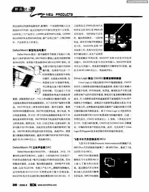
飞思卡尔半导体公司 文档编号:MC33797技术数据第6.0版,2014年2月©飞思卡尔半导体公司,2006 - 2014。
保留所有权利。
四通道点火驱动器IC四通道点火驱动器IC 是一款用于汽车安全气囊模块的完整点火诊断和部署接口。
拥有全面的诊断和系统控制功能,可实现故障安全操作。
该器件包含一个兼容串行外设接口(SPI)的8位接口,支持微处理器控制。
该器件可用于标准的四通道点火驱动器IC ,或用于高边和低边点火驱动器位于不同点火驱动器IC 时的交叉耦合状态。
高边和低边的输出驱动器均受到保护,不会受对电池或对地临时短路的影响。
限流阈值由外部电阻设置。
该器件采用SMARTMOS 技术。
特性 • 四通道高边和低边2.0 A FET 开关 • 外部可调的FET 限流功能 • 可调限流范围:0.8至2.0 A • 通过与SPI 通信实现单个通道限流检测以及定时持续时间测量 • 用于诊断和FET 开关激活的8位SPI • 高边安全传感器状态诊断 • 点火装置的电阻和电压诊断 • 点火驱动器IC 可用于交叉耦合驱动器点火应用(将高边和低边FET 开关置于不同的点火驱动器IC 上)EW 后缀(无铅) 98ARH99137A 32引脚SOICW应用 • 汽车安全气囊展开 • 安全带自动锁止• 计算机控制模型火箭点火器 • 远程发射烟花焰火表演• 采矿和建筑施工中计算机控制的雷管点火 •军用或警用武器系统图1. 33797简化应用电路图337972 模拟集成电路器件数据飞思卡尔半导体公司1 可订购部件表1. 可订购部件版本注1. 要订购以带/卷形式提供的零件,请在部件编号后面添加R2后缀。
内部功能框图33797模拟集成电路器件数据飞思卡尔半导体公司3内部功能框图图2.33797简化内部功能框图引脚连接337974 模拟集成电路器件数据飞思卡尔半导体公司引脚连接图3. 引脚功能说明表2. 引脚功能说明引脚连接33797模拟集成电路器件数据飞思卡尔半导体公司5表2. 引脚功能说明(续)电气特性最大额定值337976 模拟集成电路器件数据飞思卡尔半导体公司电气特性最大额定值表3. 最大额定值所有电压都是相对于地而言,除非另有说明。
Freescale Kinetis KL25系列社区资料大全及实例汇总介绍:Freescale 公司Kinetis KL25 MCU向L系列内增加了带集成低压稳压器的全速USB 2.0 OTG控制器,采用32位ARM Cortex-M0内核,拥有48MHz内核频率,工作电压为1.71V~3.6V,。
KL25系列作为低功耗、低价格、高性能的微控制器,给工程师们提供了一个合适的入门级32位方案。
本文精选了Kinetis K25教程、例程、设计案例,以及基于Kinetis KL25的流行开发板,集结了国内外官方资料和资深工程师的经验,是学习Kinetis KL25 MCU的必备宝典。
Kinetis KL25 MCU 的功能框图Kinetis KL25 MCU 教程篇Kinetis KL25 MCU官方参考手册Kinetis KL25 MCU 官方数据手册飞思卡尔Kinetis系列产品开发资源链接总汇包含Kinetis系列产品的参考手册、数据手册、编译环境、调试工具的相关资源链接。
KL25中文用户手册官方Kinetis L系列三大特性演示视频(附中文说明文档)你在设计中往往会忽略掉Kinetis L系列的重要的特性。
如果你只是简单的把Kinetis L系列当做一般的Cortex-M0的单片机来使用的话,我们的设计人员估计要郁闷了。
闲话少说,赶紧来看看你可能忽略的特性吧Cortex-M0+, 到底“+”了什么(有视频,有中文文档)飞思卡尔Kinetis L系列采用的内核是Cortex-M0+,而不是Cortex-M0。
这个小小的加号到底增加了什么呢?小小视频讲的一清二楚。
根据KL系列芯片上的缩略标志识别具体型号大家在使用kinetis芯片的时候,可能会发现一些比较小的芯片上并没有刻出芯片的具体型号,而是刻了一个缩略型号名称,那么如何根据这个缩略名称来识别具体的型号呢?文中罗列了Kinetis L系列所有的缩略型号对应的芯片具体型号名称,方便大家识别。