IXSK30N60CD1中文资料
- 格式:pdf
- 大小:72.43 KB
- 文档页数:2

The All-New i30Photos for reference only圖片只供參考N. Born in Namyang.Honed at Nürburgring.The All-New i30 N marks the premiere of the new Hyundai N high performance range. N stands for Namyang, home of our global R&D centre. Born in Namyang and honed at the Nürburgring – the N logo also symbolises a racetrack’s chicane curve. Hyundai N cars are designed to perform – and to put a grin on your face. Engineered to satisfy drivers who want to feel the burst of adrenaline that gets your heart beating faster – The pure joy of driving.全新的 i 30 N 掀起一場屬於現代的高性能革命。
N 代表位於南陽的現代汽車研發中心,生於南陽長於紐布靈,賽車血脈融貫出彎曲賽道的標誌-N 。
N系車款在乎時速快感,更在乎駕駛樂趣。
啟動引擎,激發澎湃,一下貫穿全身。
N.Nothing but fun. 純粹.快樂。
Photos for reference only圖片只供參考 fun.Created for maximum driving fun on the road, the All-New i30 N has been meticulously engineered to get your heart pumping faster. Balancing racetrack driving dynamics and raw power with the possibility of comfort-oriented daily commuting, the i30 N is truly a sports car for every day – built to make every moment behind the wheel a chance for more kicks.全新 i30 N 以細致的機械美學撼動你心,駕駛之樂由此開創。
北京科力赛克sk303说明书北京科力赛克SK303说明书一、产品概述北京科力赛克(SK)303是一款高性能的电子产品,具有多种功能和特点。
本产品使用了先进的科技技术,以满足用户对高质量产品的需求。
SK303具有稳定可靠的性能,广泛适用于各种场合。
二、功能特点1.高性能处理器:SK303采用了先进的处理器技术,能够快速、高效地处理各种任务,并保证系统的稳定性和可靠性。
2.丰富的功能:SK303具有多种功能,包括但不限于通信、娱乐、办公等。
用户可以根据自己的需求进行设置和使用。
3.人性化设计:SK303的设计考虑了用户的使用习惯和舒适度,具有人性化的界面和操作方式,方便用户使用和操作。
4.高清屏幕:SK303配备了高清屏幕,显示效果清晰,色彩鲜艳,让用户享受更好的视觉体验。
5.长续航时间:SK303采用了节能技术,能够延长电池的使用时间,提供更长久的电力支持。
三、使用方法1.开机操作:按下电源键,等待系统启动完成。
2.功能设置:根据需要,进入设置界面进行各项功能的设置,如网络连接、声音调节、屏幕亮度等。
3.应用程序:根据个人需求,选择并打开相应的应用程序,进行各种操作和使用。
4.关机操作:在使用完毕后,按住电源键,选择关机选项,等待系统关机完成。
四、注意事项1.避免过度使用:长时间连续使用SK303可能会导致过热,建议适当休息。
2.保护屏幕:请勿使用尖锐物体或过度力量触碰或按压屏幕,以防刮伤或破裂。
3.防止水潮湿:请保持SK303远离水源,避免进水或受潮,以防损坏内部电路。
4.存储环境:请保持SK303存放在干燥、清洁的环境中,避免灰尘或湿气对产品的影响。
5.保养维护:定期清洁SK303的外壳和屏幕,避免灰尘或污渍积累。
五、售后服务1.保修期:SK303享受一年的免费保修服务,保修期内出现质量问题可免费维修或更换。
2.售后服务:如需维修或咨询服务,请联系北京科力赛克客服,提供详细的产品信息和问题描述,我们会尽快为您解决问题。
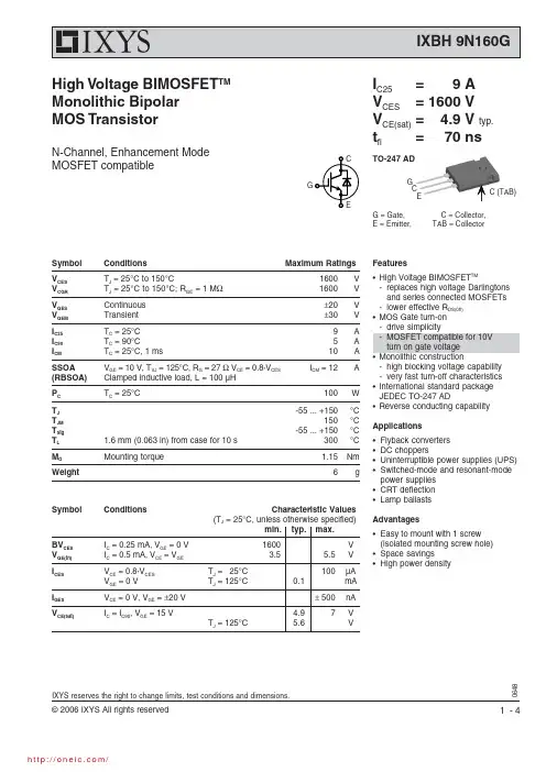
648IXYS reserves the right to change limits, test conditions and dimensions.High Voltage BIMOSFET TM Monolithic Bipolar MOS TransistorN-Channel, Enhancement Mode MOSFET compatibleSymbol ConditionsCharacteristic Values(T J = 25°C, unless otherwise specified)min.typ.max.BV CES I C = 0.25 mA, V GE = 0 V 1600V V GE(th)I C = 0.5 mA, V CE = V GE 3.55.5V I CES V CE = 0.8·V CES T J =25°C 100µA V GE = 0 VT J =125°C0.1mA I GES V CE = 0 V, V GE = ±20 V± 500nA V CE(sat)I C = I C90, V GE = 15 V4.97V T J =125°C5.6VSymbol ConditionsMaximum RatingsV CES T J = 25°C to 150°C1600V V CGR T J = 25°C to 150°C; R GE = 1 M Ω1600V V GES Continuous ±20V V GEM Transient ±30V I C25T C = 25°C 9A I C90T C = 90°C5A I CMT C = 25°C, 1 ms10A SSOA V GE = 10 V, T VJ = 125°C, R G = 27 Ω V CE = 0.8·V CES I CM = 12A (RBSOA)Clamped inductive load, L = 100 µH P C T C = 25°C100W T J -55 ... +150°C T JM 150°C T stg -55 ... +150°C T L 1.6 mm (0.063 in) from case for 10 s 300°C M d Mounting torque1.15Nm Weight6gFeatures•High Voltage BIMOSFET TM-replaces high voltage Darlingtons and series connected MOSFETs -lower effective R DS(on)•MOS Gate turn-on -drive simplicity-MOSFET compatible for 10V turn on gate voltage •Monolithic construction-high blocking voltage capability -very fast turn-off characteristics •International standard package JEDEC TO-247 AD•Reverse conducting capability Applications •Flyback converters •DC choppers•Uninterruptible power supplies (UPS)•Switched-mode and resonant-mode power supplies •CRT deflection •Lamp ballasts Advantages•Easy to mount with 1 screw (isolated mounting screw hole)•Space savings •High power densityGTO-247 ADGC EG = Gate, C = Collector,E = Emitter,TAB = CollectorC (TAB)I C25=9A V CES =1600V V CE(sat)= 4.9V typ.t fi =70ns648IXYS reserves the right to change limits, test conditions and dimensions.TO-247 AD OutlineDim. Millimeter Inches Min.Max.Min.Max.A 19.8120.320.7800.800B 20.8021.460.8190.845C 15.7516.260.6100.640D 3.55 3.650.1400.144E 4.32 5.490.1700.216F 5.4 6.20.2120.244G 1.65 2.130.0650.084H - 4.5-0.177J 1.0 1.40.0400.055K 10.811.00.4260.433L 4.7 5.30.1850.209M 0.40.80.0160.031N1.52.490.0870.102SymbolConditionsCharacteristic Values(T = 25°C, unless otherwise specified)C ies C oes V CE = 25 V, V C res Q g I C = 5 A, V CE = 600 V, V d(on)ri d(off)fi R thJC R thCKReverse ConductionInductive load, T I C = I C90, V GE = 10 V, L = 100 µH,V CE = 960 V, R648IXYS reserves the right to change limits, test conditions and dimensions.V CE - Volts40080012001600I C M - A m p e r e s051015V F - Volts246810I F - A m p e r e s51015202530Q G - nanocoulombs1020304050V G E - V o l t s0246810121416V CE - Volts024681012141618I C - A m p e r e s51015202530T J = 25°CV GE - Volts 468101214I C - A m p e r e s51015202530V CE - Volts 024681012141618I C - A m p e r e s51015202530V GE Fig. 1Typ. Output CharacteristicsFig. 2Typ. Output CharacteristicsFig. 3Typ. Transfer CharacteristicsFig. 4Typ. Characteristics of ReverseConductionFig. 5Typ. Gate Charge characteristicsFig. 6Reverse Biased Safe Operating AreaRBSOA648IXYS reserves the right to change limits, test conditions and dimensions.I C - Amperes246810121416t f i - n a n o s e c o n d s406080100120140R g - Ohms102030405060t d (o f f )- n a n o s e c o n d s50100150200250Pulse Width - Seconds0.000010.00010.0010.010.11Z t h J C - K /W0.0010.010.1110Fig. 7Typ. Fall TimeFig. 8Typ. Turn Off Delay TimeFig. 9Typ. Transient Thermal Impedance分销商库存信息: IXYSIXBH9N160G。
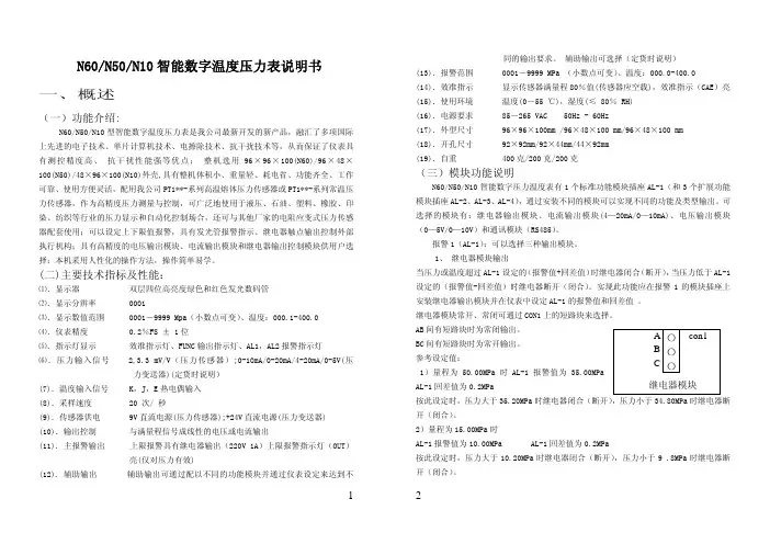
N60/N50/N10智能数字温度压力表说明书 一、概述(一)功能介绍:N60/N50/N10型智能数字温度压力表是我公司最新开发的新产品,融汇了多项国际上先进的电子技术、单片计算机技术、电擦除技术、抗干扰技术等,从而保证了仪表具有测控精度高、 抗干扰性能强等优点; 整机选用96×96×100(N60)/96×48×100(N50)/48×96×100(N10)外壳,具有整机体积小、重量轻、耗电省、功能齐全、工作可靠、使用方便灵活,配用我公司PT1**-系列高温熔体压力传感器或PT1**-系列常温压力传感器,作为高精度压力测量与控制,可广泛地使用于液压、石油、塑料、橡胶、印染、纺织等行业的压力显示和自动化控制场合,还可与其他厂家的电阻应变式压力传感器配套使用;可以设定上下限值报警,具有发光管报警指示、继电器触点输出控制外部执行机构;具有高精度的电压输出模块、电流输出模块和继电器输出控制模块供用户选择;本机采用人性化的操作方法,操作简单易学。
(二)主要技术指标及性能:⑴.显示器 双层四位高亮度绿色和红色发光数码管⑵.显示分辨率 0001⑶.显示数值范围 0001-9999 Mpa(小数点可变)、温度:000.1-400.0⑷.仪表精度 0.2%FS ± 1位⑸.指示灯显示 效准指示灯、FUNC输出指示灯、AL1,AL2报警指示灯⑹.压力输入信号 2,3.3 mV/V(压力传感器);0-10mA/0-20mA/4-20mA/0-5V(压力变送器)(定货时说明)(7).温度输入信号 K,J,E热电偶输入(8).采样速度 20 次/ 秒(9).传感器供电 9V直流电源(压力传感器);+24V直流电源(压力变送器)(10).输出控制 与满量程信号成线性的电压或电流输出(11).主报警输出 上限报警具有继电器输出(220V 1A)上限报警指示灯(OUT)亮(仅对压力有效)(12). 辅助输出 辅助输出可通过配以不同的功能模块并通过仪表设定来达到不同的输出要求。
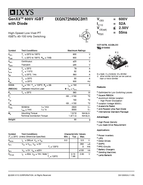
Symbol Test Conditions Characteristic Values(TJ= 25°C, Unless Otherwise Specified) Min. Typ. Max.VGE(th) IC= 250μA, VCE= VGE3.0 5.5 VI CES VCE= VCES, VGE= 0V 250μA TJ= 125°C 3 mAI GES VCE= 0V, VGE= ±20V ±100nAVCE(sat) IC= 50A, VGE= 15V, Note 1 2.10 2.50 VTJ= 125°C 1.65VCES= 600VIC110= 52AVCE(sat)≤ 2.50Vtfi(typ)= 55nsGenX3TM 600V IGBTwith DiodeHigh-Speed Low-Vsat PTIGBTs 40-100 kHz SwitchingIXGN72N60C3H1 Symbol Test Conditions Maximum RatingsVCES TJ= 25°C to 150°C600 VVCGR TJ= 25°C to 150°C, RGE= 1MΩ600 VVGESContinuous±20 VVGEMTransient±30 VI C25TC= 25°C 78 AIC110TC= 110°C52 AI CM TC= 25°C, 1ms360 AI A TC= 25°C50AEAS TC= 25°C500mJSSOA VGE = 15V, TVJ= 125°C, RG= 2Ω ICM= 150 A(RBSOA)Clamped Inductive Load @ VCE ≤ VCESPC TC= 25°C360 WTJ-55 ... +150 °CTJM150 °CTstg-55 ... +150 °CVISOL 50/60Hz t = 1min2500 V~ IISOL≤ 1mA t = 1s3000 V~Md Mounting Torque 1.5/13 Nm/lb.in.Terminal Connection Torque 1.3/11.5 Nm/lb.in. Weight30 g SOT-227B, miniBLOCG = Gate, C = Collector, E = Emitterc either emitter terminal can be used asMain or Kelvin EmitterGE cE cCE153432Featuresz Optimized for Low Switching Losses z Square RBSOAz Aluminium Nitride Isolation-High Power Dissipationz Isolation Voltage 3000V~z Avalanche Ratedz Anti-Parallel Ultra Fast Diodez International Standard Package Advantagesz High Power Densityz Low Gate Drive Requirement Applicationsz Power Invertersz UPSz Motor Drivesz SMPSz PFC Circuitsz Battery Chargersz Welding Machinesz Lamp BallastsIXYS Reserves the Right to Change Limits, Test Conditions, and Dimensions.Reverse Diode (FRED)Symbol Test ConditionsCharacteristic Values Notes:1. Pulse test, t ≤ 300μs, duty cycle, d ≤ 2%.2. Switching times & energy losses may increase for higher V CE (Clamp), T J or R G .SOT-227B miniBLOCM4 screws (4x) suppliedIXYS Reserves the Right to Change Limits, Test Conditions, and Dimensions.IXYS Reserves the Right to Change Limits, Test Conditions, and Dimensions.Fig. 21Fig. 22Fig. 24Fig. 25Fig. 23。
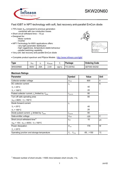
Fast IGBT in NPT-technology with soft, fast recovery anti-parallel EmCon diode• 75% lower E off compared to previous generationcombined with low conduction losses• Short circuit withstand time – 10 µs • Designed for:- Motor controls - Inverter• NPT-Technology for 600V applications offers:- very tight parameter distribution- high ruggedness, temperature stable behaviour - parallel switching capability• Very soft, fast recovery anti-parallel EmCon diode• Complete product spectrum and PSpice Models : /igbt/Type V CE I C V CE(sat )T j Package Ordering Code SKW20N60600V20A2.4V150°CTO-247ACQ67040-S4242Maximum Ratings ParameterSymbol Value Unit Collector-emitter voltage V C E600V DC collector current T C = 25°C T C = 100°CI C4020Pulsed collector current, t p limited by T jmax I C p u l s 80Turn off safe operating area V CE ≤ 600V, T j ≤ 150°C -80Diode forward current T C = 25°C T C = 100°CI F4020Diode pulsed current, t p limited by T jmax I F p u l s 80AGate-emitter voltage V G E ±20V Short circuit withstand time 1)V GE = 15V, V CC ≤ 600V, T j ≤ 150°Ct S C 10µs Power dissipation T C = 25°CP t o t179WOperating junction and storage temperatureT j , T s t g-55...+150°CP-TO-247-3-1(TO-247AC)Thermal Resistance Parameter Symbol Conditions Max. ValueUnit CharacteristicIGBT thermal resistance,junction – caseR t h J C 0.7Diode thermal resistance,junction – case R t h J C D 1.3Thermal resistance,junction – ambientR t h J ATO-247AC 40K/WElectrical Characteristic, at T j = 25 °C, unless otherwise specified ValueParameterSymbol Conditionsmin.Typ.max.UnitStatic CharacteristicCollector-emitter breakdown voltage V (B R )C E S V G E =0V, I C =500µA 600--Collector-emitter saturation voltageV C E (s a t )V G E = 15V, I C =20A T j =25°C T j =150°C1.7-22.4 2.42.9Diode forward voltageV FV G E =0V, I F =20A T j =25°C T j =150°C1.2- 1.41.25 1.81.65Gate-emitter threshold voltage V G E (t h )I C =700µA,V C E =V G E 345VZero gate voltage collector currentI C E SV C E =600V,V G E =0V T j =25°C T j =150°C----402500µAGate-emitter leakage current I G E S V C E =0V,V G E =20V --100nA Transconductance g f s V C E =20V, I C =20A -14-S Dynamic Characteristic Input capacitance C i s s -11001320Output capacitanceC o s s -107128Reverse transfer capacitance C r s s V C E =25V,V G E =0V,f =1MHz-6376pFGate chargeQ G a t e V C C =480V, I C =20A V G E =15V -100130nC Internal emitter inductancemeasured 5mm (0.197 in.) from case L E TO-247AC-13-nH Short circuit collector current1)I C (S C )V G E =15V,t S C ≤10µs V C C ≤ 600V,T j ≤ 150°C-200-ASwitching Characteristic, Inductive Load, at T j =25 °C ValueParameterSymbolConditionsmin.typ.max.UnitIGBT Characteristic Turn-on delay time t d (o n )-3646Rise timet r -3036Turn-off delay time t d (o f f )-225270Fall time t f -5465nsTurn-on energy E o n -0.440.53Turn-off energy E o f f -0.330.43Total switching energyE t sT j =25°C,V C C =400V,I C =20A,V G E =0/15V,R G =16Ω,L σ1)=180nH,C σ1)=900pFEnergy losses include “tail” and diode reverse recovery.-0.770.96mJ Anti-Parallel Diode Characteristic Diode reverse recovery timet r r t S t F---30030270---nsDiode reverse recovery charge Q r r -490-nC Diode peak reverse recovery current I r r m - 5.5-A Diode peak rate of fall of reverse recovery current during t bdi r r /dtT j =25°C,V R =200V, I F =20A,di F /dt =200A/µs-180-A/µs Switching Characteristic, Inductive Load, at T j =150 °C ValueParameterSymbolConditionsmin.typ.max.UnitIGBT Characteristic Turn-on delay time t d (o n )-3646Rise timet r -3036Turn-off delay time t d (o f f )-250300Fall time t f -6376nsTurn-on energy E o n -0.670.81Turn-off energy E o f f -0.490.64Total switching energyE t sT j =150°CV C C =400V,I C =20A,V G E =0/15V,R G =16Ω,L σ1)=180nH,C σ1)=900pFEnergy losses include “tail” and diode reverse recovery.- 1.121.45mJ Anti-Parallel Diode Characteristic Diode reverse recovery timet r r t S t F---41045365---nsDiode reverse recovery charge Q r r -1270-nC Diode peak reverse recovery current I r r m -8.5-A Diode peak rate of fall of reverse recovery current during t bdi r r /dtT j =150°CV R =200V, I F =20A,di F /dt =200A/µs-200-A/µsI C , C O L L E C T O R C U R R E N T10Hz100Hz 1kHz 10kHz 100kHz0A10A 20A 30A 40A 50A 60A 70A 80A 90A100A 110AI C , C O L L E C T O R C U R R E N T1V10V100V1000V0.1A1A10A100Af , SWITCHING FREQUENCYV CE , COLLECTOR -EMITTER VOLTAGE Figure 1. Collector current as a function of switching frequency(T j ≤ 150°C, D = 0.5, V CE = 400V,V GE = 0/+15V, R G = 16Ω)Figure 2. Safe operating area (D = 0, T C = 25°C, T j ≤ 150°C)P t o t , P O W E R D I S S I P A T I O N25°C50°C75°C100°C125°C0W 20W 40W 60W 80W 100W 120W 140W160W180W 200W I C , C O L L E C T O R C U R R E N T25°C50°C 75°C 100°C 125°C0A10A20A30A40A50AT C , CASE TEMPERATURET C , CASE TEMPERATUREFigure 3. Power dissipation as a function of case temperature (T j ≤ 150°C)Figure 4. Collector current as a function of case temperature(V GE ≤ 15V, T j ≤ 150°C)I C , C O L L E C T O R C U R R E N T0V1V 2V 3V 4V 5V0A 10A 20A 30A 40A 50A 60AI C , C O L L E C T O R C U R R E N T0V1V 2V 3V 4V 5V0A 10A20A30A40A50A60AV CE , COLLECTOR -EMITTER VOLTAGEV CE , COLLECTOR -EMITTER VOLTAGEFigure 5. Typical output characteristics (T j = 25°C)Figure 6. Typical output characteristics (T j = 150°C)I C , C O L L E C T O R C U R R E N T0V2V 4V 6V 8V 10V0A 10A 20A 30A 40A 50A 60A70A V C E (s a t ), C O L L E C T O R -E M I T T E R S A T U R A T I O N V O L T A G E-50°C 0°C 50°C 100°C 150°C1.0V1.5V2.0V2.5V3.0V3.5V4.0VV GE , GATE -EMITTER VOLTAGET j , JUNCTION TEMPERATUREFigure 7. Typical transfer characteristics (V CE = 10V)Figure 8. Typical collector-emittersaturation voltage as a function of junction temperature (V GE = 15V)t , S W I T C H I N G T I M E S10A 20A 30A 40A10ns100nst , S W I T C H I N G T I M E S0Ω10Ω20Ω30Ω40Ω50Ω60Ω10ns100nsI C , COLLECTOR CURRENTR G , GATE RESISTORFigure 9. Typical switching times as a function of collector current(inductive load, T j = 150°C, V CE = 400V,V GE = 0/+15V, R G = 16Ω,Dynamic test circuit in Figure E)Figure 10. Typical switching times as a function of gate resistor(inductive load, T j = 150°C, V CE = 400V,V GE = 0/+15V, I C = 20A,Dynamic test circuit in Figure E)t , S W I T C H I N G T I M E S0°C50°C 100°C 150°C10ns100nsV G E (t h ), G A T E -E M I T T E R T H R E S H O L D V O L T A G E-50°C0°C50°C100°C150°C 2.0V2.5V3.0V 3.5V4.0V 4.5V5.0V 5.5VT j , JUNCTION TEMPERATURET j , JUNCTION TEMPERATUREFigure 11. Typical switching times as a function of junction temperature(inductive load, V CE = 400V, V GE = 0/+15V,I C = 20A, R G = 16Ω,Dynamic test circuit in Figure E)Figure 12. Gate-emitter threshold voltage as a function of junction temperature (I C = 0.7mA)E , S W I T C H I N G E N E R G Y L O S S E S0A10A 20A 30A 40A 50A0.0mJ0.5mJ1.0mJ1.5mJ2.0mJ2.5mJ3.0mJE ,S W I T C H I N G E N E R G Y L O S S E S0Ω10Ω20Ω30Ω40Ω50Ω60Ω0.0mJ0.5mJ1.0mJ1.5mJ2.0mJ2.5mJ3.0mJI C , COLLECTOR CURRENTR G , GATE RESISTORFigure 13. Typical switching energy losses as a function of collector current(inductive load, T j = 150°C, V CE = 400V,V GE = 0/+15V, R G = 16Ω,Dynamic test circuit in Figure E)Figure 14. Typical switching energy losses as a function of gate resistor(inductive load, T j = 150°C, V CE = 400V,V GE = 0/+15V, IC = 20A,Dynamic test circuit in Figure E)E , S W I T C H I N G E N E R G Y L O S S E S0°C50°C 100°C 150°C0.0mJ0.2mJ 0.4mJ 0.6mJ 0.8mJ 1.0mJ 1.2mJ 1.4mJ1.6mJZ t h J C , T R A N S I E N T T H E R M A L I M P E D A N C E1µs10µs 100µs 1ms 10ms 100ms 1s10-410-310-210-1100T j , JUNCTION TEMPERATUREt p , PULSE WIDTHFigure 15. Typical switching energy losses as a function of junction temperature (inductive load, V CE = 400V, V GE = 0/+15V,I C = 20A, R G = 16Ω,Dynamic test circuit in Figure E)Figure 16. IGBT transient thermalimpedance as a function of pulse width (D = t p / T )V G E , G A T E -E M I T T E R V O L T A G E0nC25nC 50nC 75nC 100nC 125nC0V 5V10V 15V20V25VC , C A P A C I T A N C E0V10V 20V 30V10pF100pF1nFQ GE , GATE CHARGEV CE , COLLECTOR -EMITTER VOLTAGE Figure 17. Typical gate charge (I C = 20A)Figure 18. Typical capacitance as a function of collector-emitter voltage (V GE = 0V, f = 1MHz)t s c , S H O R T C I R C U I T W I T H S T A N D T I M E10V11V 12V 13V 14V 15V0µs 5µs10µs15µs20µs25µsI C (s c ), S H O R T C I R C U I T C O L L E C T O R C U R R E N T10V12V 14V 16V 18V20V0A 50A 100A 150A 200A 250A 300A 350AV GE , GATE -EMITTER VOLTAGEV GE , GATE -EMITTER VOLTAGEFigure 19. Short circuit withstand time as a function of gate-emitter voltage (V CE = 600V, start at T j = 25°C)Figure 20. Typical short circuit collector current as a function of gate-emitter voltage (V CE ≤ 600V, T j = 150°C)t r r , R E V E R S E R E C O V E R Y T I M E100A/µs300A/µs 500A/µs 700A/µs 900A/µs0ns100ns200ns300ns400ns500ns600nsQ r r , R E V E R S E R E C O V E R Y C H A R G E100A/µs300A/µs 500A/µs 700A/µs 900A/µs0nC500nC1000nC1500nC2000nC2500nCdi F /dt , DIODE CURRENT SLOPEdi F /dt , DIODE CURRENT SLOPEFigure 21. Typical reverse recovery time as a function of diode current slope (V R = 200V, T j = 125°C,Dynamic test circuit in Figure E)Figure 22. Typical reverse recovery charge as a function of diode current slope (V R = 200V, T j = 125°C,Dynamic test circuit in Figure E)I r r , R E V E R S E R E C O V E R Y C U R R E N T100A/µs300A/µs 500A/µs 700A/µs 900A/µs0A4A8A12A16A20A24Ad i r r /d t , D I O D E P E A K R A T E O F F A L LO F R E V E R S E R E C O V E R Y C U R R E N T100A/µs300A/µs 500A/µs 700A/µs 900A/µs0A/µs200A/µs400A/µs600A/µs800A/µs1000A/µsdi F /dt , DIODE CURRENT SLOPEdi F /dt , DIODE CURRENT SLOPEFigure 23. Typical reverse recovery current as a function of diode current slope (V R = 200V, T j = 125°C,Dynamic test circuit in Figure E)Figure 24. Typical diode peak rate of fall of reverse recovery current as a function of diode current slope (V R = 200V, T j = 125°C,Dynamic test circuit in Figure E)I F , F O R W A R D C U R R E N T0.0V0.5V 1.0V 1.5V 2.0V0A 5A 10A 15A 20A25A 30A 35A 40AV F , F O R W A R D V O L T A G E-40°C 0°C 40°C 80°C 120°C1.0V1.5V2.0VV F , FORWARD VOLTAGET j , JUNCTION TEMPERATUREFigure 25. Typical diode forward current as a function of forward voltage Figure 26. Typical diode forward voltage as a function of junction temperatureZ t h J C D , T R A N S I E N T T H E R M A L I M P E D A N C E1µs10µs 100µs 1ms 10ms 100ms 1s10-3K/W10-2K/W10-1K/W 100K/Wt p , PULSE WIDTHFigure 27. Diode transient thermalimpedance as a function of pulse width (D = t p / T )dimensionssymbol[mm][inch]minmax minmax A 4.78 5.280.18820.2079B 2.29 2.510.09020.0988C 1.78 2.290.07010.0902D 1.09 1.320.04290.0520E 1.73 2.060.06810.0811F 2.67 3.180.10510.1252G 0.76 max 0.0299 maxH 20.8021.160.81890.8331K 15.6516.150.61610.6358L 5.21 5.720.20510.2252M 19.8120.680.77990.8142N 3.560 4.9300.14020.1941∅P3.610.1421Q6.126.220.24090.2449TO-247ACFigure A. Definition of switching times Figure B. Definition of switching lossesIr r m90% Ir r m10% Ir r mdi/dtFtr rIFi,vtQSQFtStFVRdi/dtr rQ=Q Qr r S F+t=t tr r S F+Figure C. Definition of diodesswitching characteristicsτ1τ2nτr r rFigure D. Thermal equivalentcircuitFigure E. Dynamic test circuitLeakage inductance Lσ=180nHand Stray capacity Cσ=900pF.Published byInfineon Technologies AG,Bereich KommunikationSt.-Martin-Strasse 53,D-81541 München© Infineon Technologies AG 2000All Rights Reserved.Attention please!The information herein is given to describe certain components and shall not be considered as warranted characteristics. Terms of delivery and rights to technical change reserved.We hereby disclaim any and all warranties, including but not limited to warranties of non-infringement, regarding circuits, descriptions and charts stated herein.Infineon Technologies is an approved CECC manufacturer.InformationFor further information on technology, delivery terms and conditions and prices please contact your nearest Infineon Technologies Office in Germany or our Infineon Technologies Representatives worldwide (see address list).WarningsDue to technical requirements components may contain dangerous substances. For information on the types in question please contact your nearest Infineon Technologies Office.Infineon Technologies Components may only be used in life-support devices or systems with the express written approval of Infineon Technologies, if a failure of such components can reasonably be expected to cause the failure of that life-support device or system, or to affect the safety or effectiveness of that device or system. Life support devices or systems are intended to be implanted in the human body, or to support and/or maintain and sustain and/or protect human life. If they fail, it is reasonable to assume that the health of the user or other persons may be endangered.。
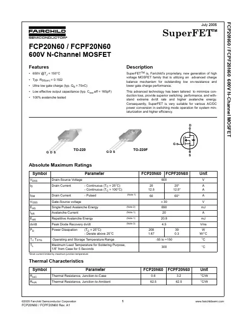
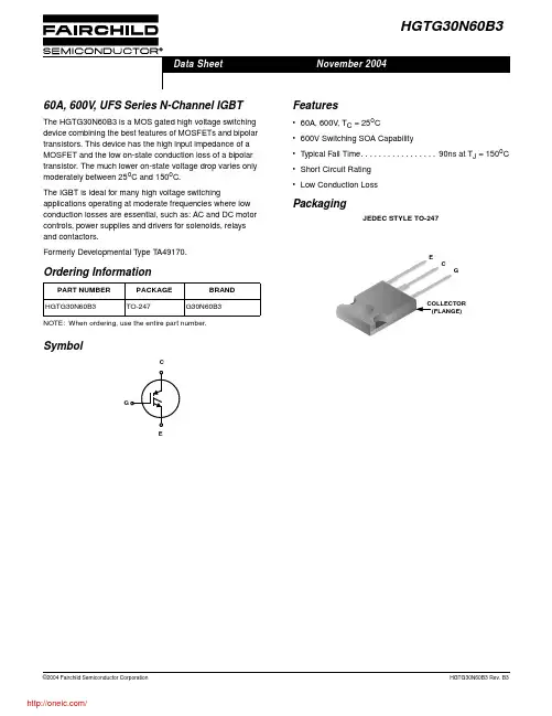
FCP20N60 / FCPF20N60 600V N-Channel MOSFETFCP20N60 / FCPF20N60 600V N-Channel MOSFETPackage Marking and Ordering InformationElectrical Characteristics T C= 25°C unless otherwise notedNotes:1. Repetitive Rating: Pulse width limited by maximum junction temperature2. I AS = 10A, V DD = 50V, R G = 25Ω, Starting T J = 25°C3. I SD ≤ 20A, di/dt ≤ 200A/µs, V DD ≤ BV DSS , Starting T J = 25°C4. Pulse Test: Pulse width ≤ 300µs, Duty Cycle ≤ 2%5. Essentially Independent of Operating Temperature Typical CharacteristicsDevice MarkingDevicePackageReel SizeTape WidthQuantityFCP20N60FCP20N60TO-220--50FCPF20N60FCPF20N60TO-220F--50SymbolParameterConditionsMinTypMax UnitsOff Characteristics BV DSS Drain-Source Breakdown Voltage V GS = 0V, I D = 250µA, T J = 25°C 600----V V GS = 0V, I D = 250µA, T J = 150°C --650--V ∆BV DSS / ∆T J Breakdown Voltage Temperature CoefficientI D = 250µA, Referenced to 25°C --0.6--V/°C BV DS Drain-Source Avalanche Breakdown VoltageV GS = 0V, I D = 20A --700--V I DSS Zero Gate Voltage Drain Current V DS = 600V, V GS = 0V V DS = 480V, T C = 125°C --------110µA µA I GSSF Gate-Body Leakage Current, Forward V GS = 30V, V DS = 0V ----100nA I GSSR Gate-Body Leakage Current, Reverse V GS = -30V, V DS = 0V -----100nA On CharacteristicsV GS(th)Gate Threshold Voltage V DS = V GS , I D = 250µA 3.0-- 5.0V R DS(on)Static Drain-Source On-ResistanceV GS = 10V, I D = 10A --0.150.19Ωg FS Forward Transconductance V DS = 40V, I D = 10A (Note 4)--17--S Dynamic CharacteristicsC iss Input Capacitance V DS = 25V, V GS = 0V,f = 1.0MHz--23703080pF C oss Output Capacitance--12801665pF C rss Reverse Transfer Capacitance --95--pF C oss Output CapacitanceV DS = 480V, V GS = 0V, f = 1.0MHz --6585pF C oss eff.Effective Output Capacitance V DS = 0V to 400V, V GS = 0V --165--pF Switching Characteristicst d(on)Turn-On Delay Time V DD = 300V, I D = 20A R G = 25Ω(Note 4, 5)--62135ns t r Turn-On Rise Time --140290ns t d(off)Turn-Off Delay Time --230470ns t f Turn-Off Fall Time --65140ns Q g Total Gate Charge V DS = 480V, I D = 20A V GS = 10V(Note 4, 5)--7598nC Q gs Gate-Source Charge --13.518nC Q gd Gate-Drain Charge--36--nC Drain-Source Diode Characteristics and Maximum RatingsI S Maximum Continuous Drain-Source Diode Forward Current ----20A I SM Maximum Pulsed Drain-Source Diode Forward Current ----60A V SD Drain-Source Diode Forward Voltage V GS = 0V, I S = 20A---- 1.4V t rr Reverse Recovery Time V GS = 0V, I S = 20AdI F /dt =100A/µs (Note 4)--530--ns Q rrReverse Recovery Charge--10.5--µCTRADEMARKSThe following are registered and unregistered trademarks Fairchild Semiconductor owns or is authorized to use and is not intended to be an exhaustive list of all such trademarks.FCP20N60 / FCPF20N60 600V N-Channel MOSFETDISCLAIMERFAIRCHILD SEMICONDUCTOR RESERVES THE RIGHT TO MAKE CHANGES WITHOUT FURTHER NOTICE TO ANY PRODUCTS HEREIN TO IMPROVE RELIABILITY, FUNCTION OR DESIGN. FAIRCHILD DOES NOT ASSUME ANY LIABILITY ARISING OUT OF THE APPLICATION OR USE OF ANY PRODUCT OR CIRCUIT DESCRIBED HEREIN; NEITHER DOES IT CONVEY ANY LICENSE UNDER ITS PATENT RIGHTS, NOR THE RIGHTS OF OTHERS.LIFE SUPPORT POLICYFAIRCHILD’S PRODUCTS ARE NOT AUTHORIZED FOR USE AS CRITICAL COMPONENTS IN LIFE SUPPORT DEVICES OR SYSTEMS WITHOUT THE EXPRESS WRITTEN APPROVAL OF FAIRCHILD SEMICONDUCTOR CORPORATION.As used herein:1. Life support devices or systems are devices or systems which,(a) are intended for surgical implant into the body, or (b) support or sustain life, or (c) whose failure to perform when properly used in accordance with instructions for use provided in the labeling,can be reasonably expected to result in significant injury to the user.2. A critical component is any component of a life support device or system whose failure to perform can be reasonably expected to cause the failure of the life support device or system, or to affect its safety or effectiveness.PRODUCT STATUS DEFINITIONS Definition of TermsDatasheet Identification Product Status DefinitionAdvance InformationFormative or In Design This datasheet contains the design specifications for product development. Specifications may change in any manner without notice.PreliminaryFirst ProductionThis datasheet contains preliminary data, andsupplementary data will be published at a later date.Fairchild Semiconductor reserves the right to make changes at any time without notice in order to improve design.No Identification Needed Full ProductionThis datasheet contains final specifications. Fairchild Semiconductor reserves the right to make changes at any time without notice in order to improve design.Obsolete Not In ProductionThis datasheet contains specifications on a product that has been discontinued by Fairchild semiconductor.The datasheet is printed for reference information only.FAST ®FASTr™FPS™FRFET™GlobalOptoisolator™GTO™HiSeC™I 2C™i-Lo ™ImpliedDisconnect™IntelliMAX™ISOPLANAR™LittleFET™MICROCOUPLER™MicroFET™MicroPak™MICROWIRE™MSX™MSXPro™OCX™OCXPro™OPTOLOGIC ®OPTOPLANAR™PACMAN™POP™Power247™PowerEdge™PowerSaver™PowerTrench ®QFET ®QS™QT Optoelectronics™Quiet Series™RapidConfigure™RapidConnect™µSerDes™SILENT SWITCHER ®SMART START™SPM™Stealth™SuperFET™SuperSOT™-3SuperSOT™-6SuperSOT™-8SyncFET™TinyLogic ®TINYOPTO™TruTranslation™UHC™UltraFET ®UniFET™VCX™Wire™ACEx™ActiveArray™Bottomless™Build it Now™CoolFET™CROSSVOLT ™DOME™EcoSPARK™E 2CMOS™EnSigna™FACT™FACT Quiet Series™Across the board. Around the world.™The Power Franchise ®Programmable Active Droop™。
Fast S-IGBT in NPT-technology with soft, fast recovery anti-parallel EmCon diode• 75% lower E off compared to previous generation combined withlow conduction losses•Short circuit withstand time – 10 µs • Designed for:- Motor controls - Inverter• NPT-Technology for 600V applications offers:- very tight parameter distribution- high ruggedness, temperature stable behaviour - parallel switching capability• Very soft, fast recovery anti-parallel EmCon diodeType V CE I C V CE(sat )T j Package Ordering Code SKP06N60600V6A2.3V150°CTO-220AB Q67040-S4230SKB06N60TO-263ABQ67040-S4231Maximum Ratings ParameterSymbol Value Unit Collector-emitter voltage V C E 600V DC collector current T C = 25°C T C = 100°CI C126.9Pulsed collector current, t p limited by T jmax I C p u l s 24Turn off safe operating area V CE ≤ 600V, T j ≤ 150°C -24Diode forward current T C = 25°C T C = 100°CI F126Diode pulsed current, t p limited by T jmax I F p u l s 24AGate-emitter voltage V G E ±20V Short circuit withstand time 1)V GE = 15V, V CC ≤ 600V, T j ≤ 150°Ct S C 10µs Power dissipation T C = 25°CP t o t 68W Operating junction and storage temperatureT j , T s t g-55...+150°C1)Allowed number of short circuits: <1000; time between short circuits: >1s.Thermal Resistance Parameter Symbol Conditions Max. ValueUnit CharacteristicIGBT thermal resistance,junction – caseR t h J C 1.85Diode thermal resistance,junction – case R t h J C D 3.5Thermal resistance,junction – ambientR t h J A TO-220AB 62SMD version, device on PCB1)R t h J ATO-263AB40K/WElectrical Characteristic, at T j = 25 °C, unless otherwise specified ValueParameterSymbol Conditionsmin.Typ.max.UnitStatic CharacteristicCollector-emitter breakdown voltage V (B R )C E S V G E =0V, I C =500µA 600--Collector-emitter saturation voltageV C E (s a t )V G E = 15V, I C =6A T j =25°C T j =150°C1.7-2.02.3 2.42.8Diode forward voltageV FV G E =0V, I F =6A T j =25°C T j =150°C1.2- 1.41.25 1.81.65Gate-emitter threshold voltage V G E (t h )I C =250µA,V C E =V G E 345VZero gate voltage collector currentI C E SV C E =600V,V G E =0V T j =25°C T j =150°C----20700µAGate-emitter leakage current I G E S V C E =0V,V G E =20V --100nA Transconductance g f s V C E =20V, I C =6A - 4.2-S Dynamic Characteristic Input capacitance C i s s -350420Output capacitanceC o s s -3846Reverse transfer capacitance C r s s V C E =25V,V G E =0V,f =1MHz-2328pFGate chargeQ G a t e V C C =480V, I C =6A V G E =15V -3242nC Internal emitter inductancemeasured 5mm (0.197 in.) from case L E TO-220AB-7-nH Short circuit collector current2)I C (S C )V G E =15V,t S C ≤10µs V C C ≤ 600V,T j ≤ 150°C-60-A 1)Device on 50mm*50mm*1.5mm epoxy PCB FR4 with 6cm 2(one layer, 70µm thick) copper area for collector connection. PCB is vertical without blown air.2)Allowed number of short circuits: <1000; time between short circuits: >1s.Switching Characteristic, Inductive Load, at T j =25 °C ValueParameterSymbolConditionsmin.typ.max.UnitIGBT Characteristic Turn-on delay time t d (o n )-2530Rise timet r -1822Turn-off delay time t d (o f f )-220264Fall time t f -5465nsTurn-on energy E o n -0.1100.127Turn-off energy E o f f -0.1050.137Total switching energyE t sT j =25°C,V C C =400V,I C =6A,V G E =0/15V,R G =50Ω,Energy losses include “tail” and diode reverse recovery.-0.2150.263mJ Anti-Parallel Diode Characteristic Diode reverse recovery timet r r t S t F---20017183---nsDiode reverse recovery charge Q r r -200-nC Diode peak reverse recovery current I r r m - 2.8-A Diode peak rate of fall of reverse recovery current during t bdi r r /dtT j =25°C,V R =200V, I F =6A,di F /dt =200A/µs-180-A/µs Switching Characteristic, Inductive Load, at T j =150 °C ValueParameterSymbolConditionsmin.typ.max.UnitIGBT Characteristic Turn-on delay time t d (o n )-2429Rise timet r -1720Turn-off delay time t d (o f f )-248298Fall time t f -7084nsTurn-on energy E o n -0.1670.192Turn-off energy E o f f -0.1530.199Total switching energyE t sT j =150°C V C C =400V,I C =6A,V G E =0/15V,R G =50ΩEnergy losses include “tail” and diode reverse recovery.-0.3200.391mJ Anti-Parallel Diode Characteristic Diode reverse recovery timet r r t S t F---29027263---nsDiode reverse recovery charge Q r r -500-nC Diode peak reverse recovery current I r r m - 5.0-A Diode peak rate of fall of reverse recovery current during t bdi r r /dtT j =150°C V R =200V, I F =6A,di F /dt =200A/µs-200-A/µsI C , C O L L E C T O R C U R R E N T10Hz100Hz 1kHz 10kHz 100kHz 0A 10A20A30AI C , C O L L E C T O R C U R R E N T1V10V100V1000V0.1A1A10Af , SWITCHING FREQUENCYV CE , COLLECTOR -EMITTER VOLTAGE Figure 1. Collector current as a function of switching frequency(T j ≤ 150°C, D = 0.5, V CE = 400V,V GE = 0/+15V, R G = 50Ω)Figure 2. Safe operating area (D = 0, T C = 25°C, T j ≤ 150°C)P t o t , P O W E R D I S S I P A T I O N25°C50°C 75°C 100°C 125°C0W 20W40W60W80WI C , C O L L E C T O R C U R R E N T25°C50°C 75°C 100°C 125°C0A5A10A15AT C , CASE TEMPERATURET C , CASE TEMPERATUREFigure 3. Power dissipation as a function of case temperature (T j ≤ 150°C)Figure 4. Collector current as a function of case temperature(V GE ≤ 15V, T j ≤ 150°C)I C , C O L L E C T O R C U R R E N T0V1V 2V 3V 4V 5V0A 5A 10A15A 20AI C , C O L L E C T O R C U R R E N T0V1V 2V 3V 4V 5V0A 5A10A15A20AV CE , COLLECTOR -EMITTER VOLTAGEV CE , COLLECTOR -EMITTER VOLTAGEFigure 5. Typical output characteristics (T j = 25°C)Figure 6. Typical output characteristics (T j = 150°C)I C , C O L L E C T O R C U R R E N T0V2V4V6V8V 10V0A 2A 4A 6A 8A 10A 12A 14A 16A18A20A V C E (s a t ), C O L L E C T O R -E M I T T E R S A T U R A T I O N V O L T A G E-50°C 0°C 50°C 100°C 150°C1.0V1.5V2.0V2.5V3.0V3.5V4.0VV GE , GATE -EMITTER VOLTAGET j , JUNCTION TEMPERATUREFigure 7. Typical transfer characteristics(V CE = 10V)Figure 8. Typical collector-emittersaturation voltage as a function of junction temperature (V GE = 15V)t , S W I T C H I N G T I M E S0A3A6A9A12A15A10ns100nst , S W I T C H I N G T I M E S0Ω50Ω100Ω150Ω10ns 100nsI C , COLLECTOR CURRENTR G , GATE RESISTORFigure 9. Typical switching times as a function of collector current(inductive load, T j = 150°C, V CE = 400V,V GE = 0/+15V, R G = 50Ω)Figure 10. Typical switching times as a function of gate resistor(inductive load, T j = 150°C, V CE = 400V,V GE = 0/+15V, I C = 6A)t , S W I T C H I N G T I M E S0°C50°C100°C150°C10ns100nsV G E (t h ), G A T E -E M I T T E R T H R E S H O L D V O L T A G E-50°C0°C50°C100°C150°C 2.0V2.5V3.0V 3.5V4.0V 4.5V5.0V 5.5VT j , JUNCTION TEMPERATURET j , JUNCTION TEMPERATUREFigure 11. Typical switching times as a function of junction temperature(inductive load, V CE = 400V, V GE = 0/+15V,I C = 6A, R G = 50Ω)Figure 12. Gate-emitter threshold voltage as a function of junction temperature (I C = 0.25mA)E , S W I T C H I N G E N E R G Y L O S S E S0A3A 6A 9A 12A 15A0.0mJ0.2mJ0.4mJ0.6mJ0.8mJE ,S W I T C H I N G E N E R G Y L O S S E S0Ω50Ω100Ω150Ω0.0mJ0.2mJ0.4mJ0.6mJI C , COLLECTOR CURRENTR G , GATE RESISTORFigure 13. Typical switching energy losses as a function of collector current(inductive load, T j = 150°C, V CE = 400V,V GE = 0/+15V, R G = 50Ω)Figure 14. Typical switching energy losses as a function of gate resistor(inductive load, T j = 150°C, V CE = 400V,V GE = 0/+15V, I C = 6A)E , SW I T C H I N G E N E R G Y L O S S E S0°C50°C 100°C 150°C0.0mJ0.1mJ0.2mJ0.3mJ0.4mJZ t h J C , T R A N S I E N T T H E R M A L I M P E D A N C E1µs10µs 100µs 1ms 10ms 100ms 1s10-310-210-1100T j , JUNCTION TEMPERATUREt p , PULSE WIDTHFigure 15. Typical switching energy losses as a function of junction temperature (inductive load, V CE = 400V, V GE = 0/+15V,I C = 6A, R G = 50Ω)Figure 16. IGBT transient thermalimpedance as a function of pulse width (D = t p / T )V G E , G A T E -E M I T T E R V O L T A G E0nC15nC30nC45nC0V 5V10V15V20V25VC , C A P A C I T A N C E0V10V20V30V10pF100pF1nFQ GE , GATE CHARGEV CE , COLLECTOR -EMITTER VOLTAGE Figure 17. Typical gate charge (I C = 6A)Figure 18. Typical capacitance as a function of collector-emitter voltage (V GE = 0V, f = 1MHz)t s c , S H O R T C I R C U I T W I T H S T A N D T I M E10V 11V12V13V14V15V0µs 5µs 10µs15µs 20µs 25µs I C (s c ), S H O R T C I R C U I T C O L L E C T O R C U R R E N T10V12V 14V16V 18V 20V0A 20A40A60A80A100AV GE , GATE -EMITTER VOLTAGEV GE , GATE -EMITTER VOLTAGEFigure 19. Short circuit withstand time as a function of gate-emitter voltage (V CE = 600V, start at T j = 25°C)Figure 20. Typical short circuit collector current as a function of gate-emitter voltage (V CE ≤ 600V, T j = 150°C)t r r , R E V E R S E R E C O V E R Y T I M E50A/µs 150A/µs 250A/µs 350A/µs 450A/µs 550A/µs 0ns100ns 200ns300ns400ns 500nsQ r r , R E V E R S E R E C O V E R Y C H A R G E50A/µs 150A/µs 250A/µs 350A/µs 450A/µs 550A/µs0nC200nC400nC600nC800nC1000nCdi F /dt , DIODE CURRENT SLOPEdi F /dt , DIODE CURRENT SLOPEFigure 21. Typical reverse recovery time as a function of diode current slope (V R = 200V, T j = 125°C)Figure 22. Typical reverse recovery charge as a function of diode current slope (V R = 200V, T j = 125°C)I r r , R E V E R S E R E C O V E R Y C U R R E N T50A/µs 150A/µs 250A/µs 350A/µs 450A/µs 550A/µs0A2A4A6A8A10A 12Ad i r r /d t , D I O D E P E A K R A T E O F F A L LO F R E V E R S E R E C O V E R Y C U R R E N T50A/µs150A/µs 250A/µs 350A/µs 450A/µs 550A/µs0A/µs100A/µs200A/µs300A/µs400A/µs500A/µs600A/µsdi F /dt , DIODE CURRENT SLOPEdi F /dt , DIODE CURRENT SLOPEFigure 23. Typical reverse recovery current as a function of diode current slope (V R = 200V, T j = 125°C)Figure 24. Typical diode peak rate of fall of reverse recovery current as a function of diode current slope (V R = 200V, T j = 125°C)I F , F O R W A R D C U R R E N T0.0V0.5V 1.0V 1.5V 2.0V0A 2A4A6A8A10A12AV F , F O R W A R D V O L T A G E-40°C 0°C 40°C 80°C 120°C1.0V1.5V2.0VV F , FORWARD VOLTAGET j , JUNCTION TEMPERATUREFigure 25. Typical diode forward current as a function of forward voltage Figure 26. Typical diode forward voltage as a function of junction temperatureZ t h J C D , T R A N S I E N T T H E R M A L I M P E D A N C E1µs10µs 100µs 1ms 10ms 100ms 1s10-2K/W10-1K/W100K/Wt p , PULSE WIDTHFigure 27. Diode transient thermalimpedance as a function of pulse width (D = t p / T )dimensionssymbol[mm][inch]minmax minmax A 9.7010.300.38190.4055B 14.8815.950.58580.6280C 0.650.860.02560.0339D 3.55 3.890.13980.1531E 2.60 3.000.10240.1181F 6.00 6.800.23620.2677G 13.0014.000.51180.5512H 4.35 4.750.17130.1870K 0.380.650.01500.0256L 0.951.320.03740.0520M 2.54 typ.0.1 typ.N 4.30 4.500.16930.1772P 1.17 1.400.04610.0551T2.302.720.09060.1071TO-220ABdimensionssymbol[mm][inch]minmax minmax A 9.8010.200.38580.4016B 0.70 1.300.02760.0512C 1.00 1.600.03940.0630D 1.03 1.070.04060.0421E 2.54 typ.0.1 typ.F 0.650.850.02560.0335G 5.08 typ.0.2 typ.H 4.30 4.500.16930.1772K 1.17 1.370.04610.0539L 9.059.450.35630.3720M 2.30 2.500.09060.0984N 15 typ.0.5906 typ.P 0.000.200.00000.0079Q 4.20 5.200.16540.2047R 8° max 8° maxS 2.40 3.000.09450.1181T 0.400.600.01570.0236U 10.800.4252V 1.150.0453W 6.230.2453X 4.600.1811Y 9.400.3701TO-263AB (D 2Pak)Z16.150.6358Figure A. Definition of switching timesIr r m90% Ir r m10% Ir r mdi/dtFtr rIFi,vtQSQFtStFVRdi/dtr rQ=Q Qr r S F+t=t tr r S F+Figure C. Definition of diodesswitching characteristicsτ1τ2nτr r rFigure D. Thermal equivalentcircuitFigure B. Definition of switching lossesPublished byInfineon Technologies AG,Bereich KommunikationSt.-Martin-Strasse 53,D-81541 München© Infineon Technologies AG 2000All Rights Reserved.Attention please!The information herein is given to describe certain components and shall not be considered as warranted characteristics. Terms of delivery and rights to technical change reserved.We hereby disclaim any and all warranties, including but not limited to warranties of non-infringement, regarding circuits, descriptions and charts stated herein.Infineon Technologies is an approved CECC manufacturer.InformationFor further information on technology, delivery terms and conditions and prices please contact your nearest Infineon Technologies Office in Germany or our Infineon Technologies Representatives worldwide (see address list).WarningsDue to technical requirements components may contain dangerous substances. For information on the types in question please contact your nearest Infineon Technologies Office.Infineon Technologies Components may only be used in life-support devices or systems with the express written approval of Infineon Technologies, if a failure of such components can reasonably be expected to cause the failure of that life-support device or system, or to affect the safety or effectiveness of that device or system. Life support devices or systems are intended to be implanted in the human body, or to support and/or maintain and sustain and/or protecthuman life. If they fail, it is reasonable to assume that the health of the user or other persons may be endangered.。
常用高清行管和大功率三极管主要参数资料高清彩电行管损坏的原因及代换现在,大屏幕彩色电视大都是数字高清,原来50Hz的场扫描频率接近人眼感知频闪的临界点,所以高清电视都是提高扫描频率来提高图像的清晰度,即将场扫描提高到100Hz或是60Hz逐行,这样就会使行扫描的频率提高一倍,自然行输出管的开关速度和功耗都会随之增加,普通的行输出管已经不能胜任,要采用性能更好的大功率三极管。
目前采用的行管有:C5144、C5244、J6920、C5858、C5905等,这些行输出管的耐压都在1500V以上,电流多大于20A,但是由于其功耗比较大,损坏率还是比较高。
归纳起来,其损坏的原因一般有以下六种。
1. 行激励不足如果行激励不足,行管不能迅速截止与饱和,导致行管内阻变大,将造成行输出电路的功耗增加,引起行输出管发烫,一旦超过行管功耗的极限值,便会使行管烧坏。
在海信高清电视中,行振荡方波信号是由数字变频解码板输出,经过一对三极管2SC1815、2SA1015放大后,送到行激励管的基极。
这两个三极管工作在大电流开关状态,故障率相对较高,损坏后就会造成行激励不足,损坏行输出管,对比可以用示波器测量行管基极的波形来确定。
另外,行管基极的限流电阻阻值一般为0.1Ω,与行管的发射极串联,再与行激励变压器并联,若是阻值增大有可能用普通万用表测不出来。
我们曾经修过多例次电阻增值到2Ω以上而导致开机几分钟后行管损坏的故障,且损坏行管的比例较大。
2. 行逆程电压过高在行逆程期间,偏转线圈会对逆程电容充电,逆程电容容量大小决定充电的时间。
容量越小,充电时间越短,充电电压越高,因而会产生很高的反峰脉冲电压。
所以,当行一旦超过行管的耐压值,就会出现屡烧行管的结果。
我们在测量逆程电容时,一般是测量电容的直流参数,而一些ESR等交流参数无法测量,所以最好是代换较可靠。
3. 行偏转线圈或行输出变压器局部短路造成行负责过重常见场输出集成电路击穿导致行偏转线圈或行输出变压器绝缘性能下降,产生局部短路、行输出逆程电容漏电等。
1 - 2© 2000 IXYS All rights reservedTO-247AD(IXSH)
High Speed IGBT with DiodeIXSH 30 N60CD1IXSK 30 N60CD1IXST 30 N60CD1
Short Circuit SOA Capability
GCE
G = GateC = CollectorE = EmitterTAB = Collector
SymbolTest ConditionsMaximum RatingsVCESTJ= 25°C to 150°C600VVCGRTJ= 25°C to 150°C; RGE = 1 MW600VVGESContinuous±20VVGEMTransient±30VIC25TC= 25°C55AIC90TC= 90°C30AICMTC= 25°C, 1 ms110ASSOAVGE= 15 V, TJ = 125°C, RG = 10 W ICM = 60A(RBSOA)Clamped inductive load, VCL = 0.8 VCES
tSCVGE= 15 V, VCE = 360 V, TJ = 125°C 10ms(SCSOA)RG = 33 W, non repetitive
PCTC= 25°C200WTJ-55 ... +150°CTJM150°CTstg-55 ... +150°CMdMounting torque1.13/10Nm/lb.in.Weight6gMaximum lead temperature for soldering300°C1.6 mm (0.062 in.) from case for 10 s
SymbolTest ConditionsCharacteristic Values(TJ = 25°C, unless otherwise specified)min.typ.max.
BVCESIC= 750 mA, VGE = 0 V600VVGE(th)IC= 2.5 mA, VCE = VGE47V
ICESVCE= 0.8 • VCESTJ = 25°C200mAVGE= 0 VTJ = 125°C3mA
IGESVCE= 0 V, VGE = ±20 V±100nAVCE(sat)VGE = 15 VIC = IC902.5V
Features•International standard packages:JEDEC TO-247, TO-264& TO-268•Short Circuit SOA capability•High freqeuncy IGBT and anti-parallel FRED in one package•New generation HDMOSTM process
Applications•AC motor speed control•DC servo and robot drives•DC choppers•Uninterruptible power supplies (UPS)•Switch-mode and resonant-modepower supplies
Advantages•Space savings (two devices in onepackage)•Easy to mount with 1 screw(isolated mounting screw hole)•Surface mountable, high power casestyle•Reduces assembly time and cost•High power density
98518A (7/00)
VCES=600 VIC25=55 A
VCE(sat)=2.5 V
tfi=70 ns
TO-268 (D3)(IXST)
GCE
GCE
TO-264(IXSK)
IXYS reserves the right to change limits, test conditions, and dimensions.
Preliminary data元器件交易网www.cecb2b.com2 - 2© 2000 IXYS All rights reserved
SymbolTest ConditionsCharacteristic Values(TJ = 25°C, unless otherwise specified)min.typ.max.
gfsIC= IC90; VCE = 10 V,10SPulse test, t £ 300 ms, duty cycle £ 2 %
Cies3100pFCoesVCE = 25 V, VGE = 0 V, f = 1 MHz240pFCres50pF
Qg100nCQgeIC = IC90, VGE = 15 V, VCE = 0.5 VCES30nCQgc38nC
td(on)30nstri30nstd(off)90150nstfi70120nsEoff0.71.2mJ
td(on)35nstri35nsEon0.5mJtd(off)150nstfi140nsEoff1.2mJ
RthJC0.62K/WRthCKTO-2470.25K/WRthCKTO-2640.15K/W
Reverse Diode (FRED)Characteristic Values(TJ = 25°C, unless otherwise specified)SymbolTest Conditionsmin.typ.max.
VFIF = IC90, VGE = 0 VTJ = 150OC1.7VNote 2TJ = 150OC2.5V
IRMIF = 100A; VGE = 0 V; TJ = 100°C22.5AVR = 100 V; -diF/dt = 100 A/ms
trrIF = 1 A; -di/dt = 100 A/ms; VR = 30 VTJ =25°C3550nsRthJC1.0K/W
Inductive load, TJ = 125°CIC = IC90; VGE = 15 VVCE = 0.8 VCES; RG = 4.7 WNote 1
Inductive load, TJ = 25°CIC = IC90; VGE = 15 VVCE = 0.8 VCES; RG = 4.7 WNote 1.
IXSH30N60CD1 IXSK30N60CD1 IXST30N60CD1
Notes:1. Switching times may increase for VCE (Clamp) > 0.8 • VCES, higher TJ or increased RG.2. Pulse test, t £ 300 ms, duty cycle d £ 2 %
TO-247 AD (IXSH) Outline Dim.MillimeterInchesMin.Max.Min.Max.
A19.8120.320.7800.800B20.8021.460.8190.845
C15.7516.260.6100.640D3.553.650.1400.144
E4.325.490.1700.216F5.46.20.2120.244
G1.652.130.0650.084H-4.5-0.177
J1.01.40.0400.055K10.811.00.4260.433
L4.75.30.1850.209M0.40.80.0160.031
N1.52.490.0870.102
Dim.MillimeterInchesMin.Max.Min.Max.
A4.95.1.193.201A12.72.9.106.114A2.02.25.001.010
b1.151.45.045.057b21.92.1.75.83C.4.65.016.026
D13.8014.00.543.551E15.8516.05.624.632E113.313.6.524.535
e 5.45 BSC .215 BSCH18.7019.10.736.752L2.402.70.094.106
L11.201.40.047.055L21.001.15.039.045L3 0.25 BSC .010 BSCL43.804.10.150.161
TO-268AA (IXST) (D3 PAK) Min. Recommended Footprint
MillimeterInchesMin.Max.Min.Max.A4.825.13.190.202A12.542.89.100.114A22.002.10.079.083b1.121.42.044.056b12.392.69.094.106b22.903.09.114.122c0.530.83.021.033D25.9126.161.0201.030E19.8119.96.780.786e5.46 BSC.215 BSCJ0.000.25.000.010K0.000.25.000.010L20.3220.83.800.820L12.292.59.090.102P3.173.66.125.144Q6.076.27.239.247Q18.388.69.330.342R3.814.32.150.170R11.782.29.070.090S6.046.30.238.248T1.571.83.062.072Dim. TO-264 AA (IXSK) Outline
IXYS MOSFETS and IGBTs are covered by one or more of the following U.S. patents:4,835,5924,881,1065,017,5085,049,9615,187,1175,486,7154,850,0724,931,8445,034,7965,063,3075,237,4815,381,025
元器件交易网www.cecb2b.com