MAX9311中文资料
- 格式:pdf
- 大小:375.37 KB
- 文档页数:12

General DescriptionThe MAX3311/MAX3313 are low-power, +5V EIA/TIA-232-compatible transceivers. Both devices have one transmitter and one receiver. The transceivers have a proprietary low-dropout transmitter output stage enabling RS-232-compatible operation from a +5V sup-ply with a single inverting charge pump. These devices require only three 0.1µF capacitors and will run at data rates up to 460kbps while maintaining RS-232-compati-ble output levels.The MAX3311 features a 1µA shutdown mode. In shut-down the device turns off the charge pump, pulls V- to ground, and the transmitter output is disabled. The MAX3313 features an INVALID output that asserts high when an active RS-232 cable signal is connected, sig-naling to the host that a peripheral is connected to the communication port.________________________ApplicationsDigital Cameras PDAs GPS POSTelecommunications Handy Terminals Set-Top BoxesFeatureso 1µA Low-Power Shutdown (MAX3311)o INVALID Output (MAX3313)o Receiver Active in Shutdown (MAX3311)o Single Transceiver (1Tx/1Rx) in 10-Pin µMAX o RS-232-Compatible OperationMAX3311/MAX3313460kbps, 1µA Supply Current,RS-232-Compatible Transceivers in µMAX________________________________________________________________Maxim Integrated Products 1Pin Configurations19-1901; Rev 0; 2/01Ordering InformationFor price, delivery, and to place orders,please contact Maxim Distribution at 1-888-629-4642,or visit Maxim’s website at .Typical Operating CircuitM A X 3311/M A X 3313460kbps, 1µA Supply Current,RS-232-Compatible Transceivers in µMAX 2_________________________________________________________________________________________ABSOLUTE MAXIMUM RATINGSELECTRICAL CHARACTERISTICSStresses beyond those listed under “Absolute Maximum Ratings” may cause permanent damage to the device. These are stress ratings only, and functional operation of the device at these or any other conditions beyond those indicated in the operational sections of the specifications is not implied. Exposure to absolute maximum rating conditions for extended periods may affect device reliability.V CC to GND..............................................................-0.3V to +6V V- to GND.................................................................+0.3V to -7V V CC + |V-|.............................................................................+13V Input VoltagesTIN, SHDN to GND.................................................-0.3V to +6V RIN to GND........................................................................±25V Output VoltagesTOUT to GND..................................................................±13.2V ROUT, INVALID to GND.......................…-0.3V to (V CC + 0.3V)Short-Circuit DurationTOUT to GND...........................................................ContinuousContinuous Power Dissipation10-Pin µMAX (derate 5.6mW/°C above +70°C).............444mW Operating Temperature RangesMAX331_CUB.......................................................0°C to +70°C MAX331_EUB....................................................-40°C to +85°C Junction Temperature......................................................+150°C Storage Temperature Range.............................-65°C to +150°C Lead Temperature (soldering, 10s).................................+300°CMAX3311/MAX3313460kbps, 1µA Supply Current,RS-232-Compatible Transceivers in µMAX_______________________________________________________________________________________3TIMING CHARACTERISTICSELECTRICAL CHARACTERISTICS (continued)M A X 3311/M A X 3313460kbps, 1µA Supply Current,RS-232-Compatible Transceivers in µMAXTypical Operating Characteristics(V CC = +5V, 0.1µF capacitors, transmitter loaded with 3k Ωand C L , T A = +25°C, unless otherwise noted.)0428612101410001500500200025003000SLEW RATEvs. LOAD CAPACITANCELOAD CAPACITANCE (pF)S L E W R A T E (V /µs )-5-4-3-2-10123456050010001500200025003000TRANSMITTER OUTPUT VOLTAGEvs. LOAD CAPACITANCELOAD CAPACITANCE (pF)T R A N S M I T T E R O U T P U T V O L T A G E (V )010001500500200025003000SUPPLY CURRENT vs. LOAD CAPACITANCELOAD CAPACITANCE (pF)MAX3311/MAX3313460kbps, 1µA Supply Current,RS-232-Compatible Transceivers in µMAX_______________________________________________________________________________________5Detailed DescriptionSingle Charge-Pump Voltage ConverterThe MAX3311/MAX3313 internal power supply has a single inverting charge pump that provides a negative voltage from a single +5V supply. The charge pump operates in a discontinuous mode and requires a flying capacitor (C1) and a reservoir capacitor (C2) to gener-ate the V- supply.RS-232-Compatible DriverThe transmitter is an inverting level translator that con-verts CMOS-logic levels to EIA/TIA-232-compatible lev-els. It guarantees data rates up to 460kbps with worst-case loads of 3k Ωin parallel with 1000pF. When SHDN is driven low, the transmitter is disabled and put into three state. The transmitter input does not have an internal pullup resistor.RS-232 ReceiverThe MAX3311/MAX3313 receiver converts RS-232 sig-nals to CMOS-logic output levels. The MAX3311 receiv-er will remain active during shutdown mode. The MAX3313 INVALID indicates when an RS-232 signal is present at the receiver input, and therefore when the port is in use.The MAX3313 INVALID output is pulled low when no valid RS-232 signal level is detected on the receiver input.MAX3311 Shutdown ModeIn shutdown mode, the charge pump is turned off, V- is pulled to ground, and the transmitter output is disabled (Table 1). This reduces supply current typically to 1µA.The time required to exit shutdown is typically less than 100µs.Applications InformationCapacitor SelectionThe capacitor type used for C1 and C2 is not critical for proper operation; either polarized or nonpolarized capacitors are acceptable. If polarized capacitors are used, connect polarity as shown in the Typical Operating Circuit . The charge pump requires 0.1µF capacitors. Increasing the capacitor values (e.g., by afactor of 2) reduces power consumption. C2 can be increased without changing C1’s value. However, do not increase C1’s value without also increasing the value of C2 and C BYPASS to maintain the proper ratios (C1 to the other capacitors).When using the minimum 0.1µF capacitors, make sure the capacitance does not degrade excessively with temperature. If in doubt, use capacitors with a larger nominal value. The capacitor ’s equivalent series resis-tance (ESR) usually rises at low temperatures and influ-ences the amount of ripple on V-.To reduce the output impedance at V-, use larger capacitors (up to 10µF).Bypass V CC to ground with at least 0.1µF. In applica-tions sensitive to power-supply noise generated by the charge pump, decouple V CC to ground with a capaci-tor the same size as (or larger than) charge-pump capacitors C1 and C2.Transmitter Output when ExitingShutdownFigure 1 shows the transmitter output when exiting shutdown mode. The transmitter is loaded with 3k Ωin parallel with 1000pF. The transmitter output displays no ringing or undesirable transients as the MAX3311comes out of shutdown. Note that the transmitter is enabled only when the magnitude of V- exceeds approximately -3V.Figure 1. Transmitter Output when Exiting Shutdown or Powering Up10µs/divTIN = GNDTIN = V CCM A X 3311/M A X 3313High Data RatesThe MAX3311/MAX3313 maintain RS-232-compatible transmitter output voltage (±3.7V minimum) even at high data rates. Figure 2 shows a transmitter loopback test circuit. Figure 3 shows the loopback test result at 120kbps, and Figure 4 shows the same test at 250kbps.460kbps, 1µA Supply Current,RS-232-Compatible Transceivers in µMAX6_______________________________________________________________________Figure 4. Loopback Test Results at 250kbps 2µs/divFigure 3. Loopback Test Results at 120kbps5µs/divFigure 5. Receiver Positive/Negative Thresholds for INVALID-0.3V+2.7V +0.3V0INDETERMINATEINVALID HIGHINVALID LOW460kbps, 1µA Supply Current,RS-232-Compatible Transceivers in µMAXMAX3311/MAX3313Maxim cannot assume responsibility f or use of any circuitry other than circuitry entirely embodied in a Maxim product. No circuit patent licenses are implied. Maxim reserves the right to change the circuitry and specifications without notice at any time.Maxim Integrated Products, 120 San Gabriel Drive, Sunnyvale, CA 94086 408-737-7600 _____________________7©2001 Maxim Integrated ProductsPrinted USAis a registered trademark of Maxim Integrated Products.Package InformationChip InformationTRANSISTOR COUNT: 278Pin Configurations (continued)。


DatasheetFUJITSU LIFEBOOK U9311XThe Lightest Fujitsu Convertible NotebookAvailable in black and red, the new ultra-mobile FUJITSU LIFEBOOK U9311X is an ultra-light 360-degree foldable device. All-day battery runtime ensures all-day productivity, while security features such as the optional integrated PalmSecure TM palm vein sensor keep your business data protected. Powerful performance and full connectivity offer you best-in-class user experience.Maximum securityProtect your notebook and business data from unauthorized access at all times ■ Optional PalmSecure TM palm vein sensor or Fingerprint sensor ■ FHD IR Camera allows face recognition with Windows Hello ■ Kensington Lock support■ Smartcard reader and TPM 2.0■ Microsoft Secured-core PC compliantUltra-slim and lightweight designExtraordinarily lightweight design for business professionals who are always on the move■ A remarkably slim 16.9 mm convertible weighing from 1015 g with a robust magnesium housing ■ Appealing ultra-slim convertible in black or red■ The best viewing experience is guaranteed by a 13.3” FHD (1920 x 1080) display with anti-glaretouch■ Support pen input with WACOM AES technology and 4,096 pressure level, delivering ultimateprecision and controlConvenient mobility on the goHighest productivity on business trips■ All-day battery runtime offers you the exceptional mobility that you need when on the move ■ Anytime USB charge functionality to charge smartphones and other media devices, even whenthe system is powered off■ Powerful performance, thanks to integrated NVMe SSD, helping to process data fasterExcellent connectivityBe flexible and stay productive in a hyper-connected world■ Compact and versatile Thunderbolt™ 4 connector to charge your laptop, transfer files at fastspeeds, connect external monitors and other peripherals■ Full set of interfaces with a full-sized HDMI and LAN connector■ Embedded WLAN supporting Gigabit Wi-Fi 6, Bluetooth and optional 4G/LTEUse your device as a Notebook or a Tablet, depending on what you needDesigned to take your productivity to the next level, whether you’re outdoors or indoors ■ 360° foldable 2 in 1 device with 4 functional working modes ■ Pen garage with inductive charging function■ 5MP rear camera for taking pictures in tablet mode■ Quick Note Taking Button allows users to quickly activate SketchPad or StickyNote throughWindows Ink WorkspaceSpecificationProcessor Family Intel® Core™ i7-1185G7 Processor (Quad Cores, 12M Cache, 1.2 GHz, up to 4.80 GHz, Intel® vPro®)Intel® Core™ i7-1165G7 Processor (Quad Cores, 12M Cache, 1.2 GHz, up to 4.70 GHz)Intel® Core™ i5-1145G7 Processor (Quad Cores, 8M Cache, 1.1 GHz, up to 4.40 GHz, Intel® vPro®)Intel® Core™ i5-1135G7 Processor (Quad Cores, 8M Cache, 0.9 GHz, up to 4.20 GHz)Operating System1Windows 10 Pro. Fujitsu recommends Windows 10 Pro.Windows 10 Home.RAM Capacity Minimum: 8 GB LPDDR4x-4266 (Onboard); Maximum: 32 GB LPDDR4x-4266 (Onboard)Internal Storage2256 GB / 512 GB / 1 TB Value-PCIe 3.0 NVMe M.2 2280 SSD, SED/ OPAL2512 GB / 1TB PCIe 3.0 NVMe M.2 2280 SSD, SED/ OPAL2512 GB Intel® PCIe 3.0 NVMe M.2 2280 SSD with 32 GB Intel® Optane™ memory H10Display 33.8 cm (13.3”), LED backlight, FHD, Anti-glare display, Touch, UWVA, 1,920 x 1,080 pixel, 1000:1, 400 cd/m² Digitizer/ Touch Technology Wacom Digitizer 4,096-level pressure with AES pen, 10-finger multi-touch screenGraphics3Intel® Iris® Xe GraphicsLAN Intel® Ethernet Connection I219LMWLAN (Optional) Intel® Wi-Fi 6 AX201 802.11ax (2x2) and Bluetooth® 5.1Camera (Rear) 5M pixel CameraInterfaces 1 DC-in1 Combo Audio/Microphone2 Thunderbolt TM 4 (with power delivery function)2 USB 3.2 Gen 1 (1 with Anytime USB charge function)1 HDMI1 Ethernet RJ-45Expansion Slots 1 SD card slot (supports SD, SDHC, SDXC)1 SIM card slot (available when WWAN module is configured)Keyboard and Pointing Devices US/ Thai Keyboard w/backlitNumber of keyboard keys: 84, Keyboard pitch: 19 mm, Keyboard stroke: 1.5 mmPrecision touchpadAES Pen stored in pen garageQuick Note Taking ButtonSecurity Integrated Fingerprint sensor (Optional)Integrated PalmSecure TM palm vein sensor (Optional)Integrated Smartcard readerTrusted Platform Module (TPM 2.0) (Optional)Fujitsu EraseDiskFujitsu AuthConductor TM Client BasicFujitsu BIOS/ Hard Disk password protectionKensington lock slot (lock to be purchased separately)Manageability Intel® AMT (depending on processer), WOL, WOM, PXE, WFM 2.0 Compliant DMIAdditional Software Fujitsu Battery UtilityFujitsu Function Key Lock UtilityFujitsu Function ManagerFujitsu LIFEBOOK Application PanelFujitsu Mic Mute UtilityFujitsu Pointing Device UtilityFujitsu System Extension UtilitySierra Wireless Skylight (only available on devices with preconfigured WWAN)Wave MaxxAudio (Audio Enhancer)AC Adapter 19 V/ 65 W (3.42 A), 100 V – 240 V, 50 Hz – 60 Hz, 3-pin (grounded) stick typeBattery54-cell 50Wh; Up to 11 hrsQuick Charge: Up to 80% charging in 1 hourDimension (W x D x H)6309 x 214.8 x 16.9 mmWeight starting at 1015 g;(Weight may vary depending on actual configuration)Warranty 1 year warranty (depending on country); Warranty upgrades available, sold separatelyCompliance Product: LIFEBOOK U9311X; Model: 9X13A2Environmental Compliance RoHS; ENERGY STAR® 8.0, EPEAT® in progress (dedicated regions)Recommended AccessoriesAES PenAnnotate and fill in forms on your tablet with the premium FUJITSU Active Electrostatic Pen. Navigate, erase andright-click with the function button. The dedicated AES pen can be stored in the pen garage of U9311X.USB Type-C TM Port ReplicatorFlexibility, expandability, desktop replacement, investment protection 3x USB 3.2 Gen 1, DisplayPort, VGA, HDMI, RJ-45Stick-type AC AdapterPower your notebook at work, at home or on the road with a second power source. You can easily recharge your notebook everywhere. Depending on your notebook you can choose from various AC Adapters ranging from a stick type adapter to standard adapters, or even the innovative ECO AC Adapter.USB Type-C™ AC AdapterThe Fujitsu USB Type-C™ AC Adapter is compact and universal to all Fujitsu LIFEBOOKs which equip with USB Type -C™ ports, Thunderbolt™ 3 ports and Thunderbolt™ 4 ports that support power delivery function.Fujitsu PLEVIER MANASSE 15 Carrying CaseThe PLEVIER leather notebook bags which range from 14 to 15.6 inches provide high quality and aesthetically pleasing designs both to the eye and the touch. With a variety of sizes, color shades and portable carrying designs from shoulder straps to trolley belts, the bags offer maximum to cater towards your laptop devices and accessories. With inner compartments to protect against scratches, the PLEVIER leather bags offer optimal carrier designs for our device.Fujitsu Clean Desk SolutionThe Fujitsu Clean Desk is a customizable digital office with tidy, one-cable connectivity. Combining best-of-breed components from Fujitsu and its partners, the solution delivers greater well-being for users – particularly those who work all day at a display – by creating an ergonomic environment with a greater sense of space.More informationIn addition to Fujitsu LIFEBOOK U9311X, Fujitsu provides a range of platform solutions. They combine reliable Fujitsu products with the best in services, know-how and worldwide partnerships.Fujitsu PortfolioBuild on industry standards, Fujitsu offers a full portfolio of IT hardware and software products, services, solutions and cloud offering, ranging from clients to datacenter solutions and includes the broad stack of Business Solutions, as well as the full stack of Cloud offering. This allows customers to leverage from alternative sourcing and delivery models to increase their business agility and to improve their IT operation’s reliability.Computing Products/global/products/computing/Software/software/To learn more about Fujitsu LIFEBOOK U9311X, please contact your Fujitsu sales representative, Fujitsu Business partner, or visit our website.All rights reserved, including intellectual property rights. Technical data subject to modifications and delivery subject to availability. Any liability that the data and illustrations are complete, actual or correct is excluded.Designations may be trademarks and/or copyrights of the respective manufacturer, the use of which by third parties for their own purposes may infringe the rights of such owner.For further information see /terms © 2020 Fujitsu Business Technologies Asia Pacific LimitedFujitsu Green Policy Innovation is our worldwide project for reducing burdens on the environment.Using our global know-how, we aim to contribute to the creation of a sustainable environment for future generations through IT.Please find further information at/global/about/environment/Technical data are subject to modification and delivery subject to availability. Any liability that the data and illustrations are complete, actual or correct is excluded. Designations may be trademarks and/or copyrights of the respective manufacturer, the use of which by third parties for their own purposes may infringe the rights of such owner.HONG KONGFujitsu Business Technologies Asia Pacific Ltd. Tel: (852) 3910-8228Email:***********************.com /pcSINGAPOREFujitsu Asia Pte Ltd. Tel: (65) 6512-7555Email:*********************/pcCHINAFujitsu (China) Holdings Co., Ltd. – PC China Division Tel: 86 (21) 58871000-8721Email:*************************.com /pcINDONESIAPT Fujitsu Indonesia Tel: (62) 21-570-9330Email:********************.com /pcPHILIPPINESFujitsu Philippines, Inc. Tel: (63) 2-8841-8488Email:********************/pcMALAYSIAFujitsu (Malaysia) Sdn. Bhd Tel: (60) 3-8230-4188Email:*************************/pcTAIWANFujitsu Taiwan Ltd. Tel: (886) 2-2311-2255Email:************************/pcTHAILANDFujitsu (Thailand) Co., Ltd. Tel: (66) 0-2302-1500 Email:***************.com /pcVIETNAMFujitsu Vietnam Limited (Hanoi) Tel: (84-24) 2220-3113 Email:********************/pcNote: For countries not listed above, please contact our Hong Kong office.Specification disclaimersNot all features are available in all editions or versions of Windows. Systems may require upgraded and/or separately purchased hardware, drivers, software or BIOS update to take full advantage of Windows functionality. Windows 10 is automatically updated, which is always enabled. ISP fees may apply and additional requirements may apply over time for updates. GB = 1 billion bytes. TB = 1 trillion bytes, when referring to hard disk drive capacity. Accessible capacity may vary, also depending on used software. Up to 20 GB of HDD space is reserved for system recovery. Shared memory depending on main memory size and operating system. WWAN module is optional and available in specific countries/ regions only. It requires separately purchased service contract. Check with service provider for coverage and availability in your area. Connection speeds will vary due to location, environment, network conditions, and other factors. Battery runtime information is based on worldwide acknowledged BAPCo® MobileMark® 2018 (office productivity). Refer to for additional details. The BAPCo® MobileMark® Benchmark provides results that enable direct product comparisons between manufacturers. It does not guarantee any specific battery runtime which actually can be lower and may vary depending on product model, configuration, application and power management settings. The battery capacity decreases slightly with every re-charge and over its lifetime. The stated thickness does not include rubber feet.FUJITSU shall not be liable for technical or editorial errors or omissions contained herein. Ultrabook, Celeron, Celeron Inside, Core Inside, Intel, Intel Logo, Intel Atom, Intel Atom Inside, Intel Core, Intel Inside, Intel Inside Logo, Intel vPro, Intel Evo, Itanium, Itanium Inside, Pentium, Pentium Inside, vPro Inside, Xeon, Xeon Phi, Xeon Inside, Intel Agilex, Arria, Cyclone, Movidius, eASIC, Enpirion, Iris, MAX, Intel RealSense, Stratix, and Intel Optane are trademarks of Intel Corporation or its subsidiaries. USB Type-C™ and USB -C™ are trademarks of USB Implementers Forum. All other trademarks are the property of their respective owners.All rights reserved, including intellectual property rights. Technical data subject to modifications and delivery subject to availability. Any liability that the data and illustrations are complete, actual or correct is excluded. Designations may be trademarks and/or copyrights of the respective manufacturer, the use of which by third parties for their own purposes may infringe the rights of such owner. For further information see /terms . © 2020 Fujitsu Business Technologies Asia Pacific Limited Last Update: 29December 2020。

电压-频率变换器LM331LM331是美国NS公司生产的性能价格比较高的集成芯片。
LM331可用作精密的频率电压(F/V)转换器、A/D转换器、线性频率调制解调、长时间积分器以及其他相关的器件。
LM331为双列直插式8脚芯片,其引脚如图3所示。
LM331内部有(1)输入比较电路、(2)定时比较电路、(3)R-S触发电路、(4)复零晶体管、(5)输出驱动管、(6)能隙基准电路、(7)精密电流源电路、(8)电流开关、(9)输出保护点路等部分。
输出管采用集电极开路形式,因此可以通过选择逻辑电流和外接电阻,灵活改变输出脉冲的逻辑电平,从而适应TTL、DTL和CMOS 等不同的逻辑电路。
此外,LM331可采用单/双电源供电,电压范围为4~40V,输出也高达40V。
引脚1(PIN1)为电流源输出端,在f0(PIN3)输出逻辑低电平时,电流源IR输出对电容CL充电。
引脚2(PIN2)为增益调整,改变RS的值可调节电路转换增益的大小。
引脚3(PIN3)为频率输出端,为逻辑低电平,脉冲宽度由Rt和Ct决定。
引脚4(PIN4)为电源地。
引脚5(PIN5)为定时比较器正相输入端。
引脚6(PIN6)为输入比较器反相输入端。
引脚7(PIN7)为输入比较器正相输入端。
引脚8(PIN8)为电源正端。
LM331频率电压转换器V/F变换和F/V变换采用集成块LM331,LM331是美国NS公司生产的性能价格比较高的集成芯片,可用作精密频率电压转换器用。
LM331采用了新的温度补偿能隙基准电路,在整个工作温度范围内和低到4.0V电源电压下都有极高的精度。
同时它动态范围宽,可达100dB;线性度好,最大非线性失真小于0.01%,工作频率低到0.1Hz时尚有较好的线性;变换精度高,数字分辨率可达12位;外接电路简单,只需接入几个外部元件就可方便构成V/F或F/V等变换电路,并且容易保证转换精度。
图2是由LM331组成的电压频率变换电路,LM331内部由输入比较器、定时比较器、R-S触发器、输出驱动、复零晶体管、能隙基准电路和电流开关等部分组成。

MAX9217/MAX9218视频链路中的音频数据传输MAX9217/MAX9218串行器和解串器芯片组通过一对儿双绞线LVDS链路实现视频数据传输,广泛用于汽车和工业应用领域。
视频信号的每一帧总是存在消隐周期,可以利用这些周期“承载”音频数据。
在本应用笔记中,我们讨论音频数据的传输格式,视频链路发送数据的方法以及系统实现的具体实例。
简介MAX9217/MAX9218芯片组是一个收发器对儿,发送器(MAX9217)将并行数据转换成串行数据,发送给接收器(MAX9218);接收器再将串行数据转换成并行数据。
该芯片组设计用于通过一对儿低成本双绞线电缆(如,以太网中常用的UTP-CAT5电缆),将视频和控制信号从图形控制器(处理器)传输到LCD或等离子平面显示器。
传输距离可超过10米。
该芯片组链路结构简单,所使用的传输线为低成本电缆,是汽车、仪表、医疗设备等视频显示的理想方案。
该芯片组不仅可以在两点之间传送视频信号,有时,人们还希望其同时传送音频信号。
在本应用笔记中,我们将讨论如何利用视频信号的消隐期,通过控制信号通道将音频数据传送到显示器。
我们还将解释怎样把数字音频数据转换成模拟音频信号,并给出了显示面板端扬声器驱动的系统结构。
MAX9217/MAX9218链路功能和视频数据格式MAX9217串行器具有27位并行输入,总线速率高达35Mbps。
在这27位中,18位是视频RGB数据:3基色各占用6位,其余9位是控制信号。
9位控制信号中的前3位指定为垂直、水平和RGB数据同步:VSYNC (C0)、HSYNC (C1)和ENAB (C2)。
剩下的6个控制位(C3至C8)用于其他控制信号。
本例中,我们使用6个控制位中的一部分传输音频数据。
MAX9217可以将18位RGB数据或9位控制数据转换为串行数据,然后通过LVDS 链路对其进行传输。
在视频显示的消隐期内发送控制数据,由RGB数据使能信号(ENAB)指示。


M A X912/M A X913————单/双路,超高速,低功耗,精密的TTL比较器1.总体描述MAX913(单)和MAX912(双)高速,低功耗比较器是一个拥有独特设计就是在其线性区域是它的比较是可以防止振荡。
没有要求最低输入转换率。
它是由差分输入和互补的TTL输出。
快速传播延迟(10ns的典型值),具有极低的电源电流和宽共模输入范围,包括负电流使MAX912/MAX913达到的低功耗理想效果,高速,单电源+5V(或±5V)的应用,例如有V/F转换器和开关稳压器。
MAX912/MAX913保持着稳定的线性区域输出。
此功能消除了常见的在输出不稳定时产生高速驱动时具有的比较滞销输入信号。
该MAX912/MAX913可以单一+5V电源供电或±5V的分别供应。
该MAX913是一个改进的LT1016的替代品。
在输入一小能量时它提供了更宽的输入电压范围和等效速度。
在MAX912双比较具有同等性能的MAX913并且包括独立的锁存控制功能。
2.应用过零检测器以太网线接收器开关稳压器高速采样电路高速触发器扩展范围的V/F转换器快速脉冲宽度/高度的判别3.特点超快速(为10ns)单+5V或±5V的双电源供电输入范围扩展至负电源以下低功耗:6毫安(+5V)的每次比较无最小输入信号摆率的要求无电源电流扣球稳定的线性区可投入任一电源低失调电压:0.8mV4.引脚配置顶视图:5.绝对最大额定值:正电源电压 (7V)负电源电压..............................................-7V差分输入电压.......................................±15V输入电压....................................-0.3V至15V锁存引脚电压...................................等于耗材连续输出电流.....................................±20mA连续功耗(TA=70℃)8引脚塑料DIP(减少9.09mW/妹高于70°)......727mW 8引脚SO(减少5.88mW/每高于70°).................471mW 8引脚CERDIP(减少8.00mW/每高于70°).........640mW 16引脚塑料DIP(减少10.53mW/高于70°).......842mW 16引脚窄的SO(减免8.70mW/高于70°)..........696mW16引脚CERDIP(减免10.00mW/高于70°)..........800mW工作温度范围:MAX91C......................................................0℃至70℃MAX91E....................................................-40℃至85℃MAX91MJ.................................................-55℃至125℃储存温度范围........................................-65°C至150°C焊接温度(10秒).........................................................300℃注:超越“绝对最大额定值“,即可能造成永久性损坏设备。


```````````````````````````````````গၤNBY:925ဵጙࢅ߅۾Ăອᒠ൱యज़हࡍLjดᒙᔈࣅᐐፄ఼ᒜ)BHD*ጲૺࢅᐅဉ൱యज़ມᒙăকୈૹ߅ࢅᐅဉ༄ᒙहࡍĂభܤᐐፄहࡍ)WHB*Ăၒ߲हࡍĂ൱యज़ມኹखညጲૺBHD఼ᒜ࢟വăࢅᐅဉ༄ᒙहࡍࡼᐐፄৼࢾᆐ23eCLjऎWHBᐐፄభጲোၒ߲࢟ኹਜ਼BHDඡሢᏴ31eCਜ਼1eCᒄମᔈࣅࢯஂăၒ߲हࡍᎌ9eCĂ29eCਜ਼39eCྯᒬభኡᐐፄăᏴᎌኹჁࡼᄟୈሆLjहࡍೊభဧᔐᐐፄࡉࡵ51eCĂ61eC71eCăྯზၫᔊၒྜྷܠ߈ᒙၒ߲हࡍࡼᐐፄăᅪݝ࢟ᔜॊኹ఼ᒜBHDඡሢLjৈ࢟ྏభᒙࣅ0ျहဟମăྯზၫᔊၒྜྷથభܠ߈ᒙࣅᎧျहဟମࡼ܈LjBHDࡼۣߒဟମৼࢾᒋᆐ41ntăࢅᐅဉ൱యज़ມᒙखညถᆐࡍࣶၫᓘᄏ൱యज़ᄋມኹăNBY:925ݧஂဏహମࡼ25୭UEGOॖᓤăকୈਖࢾᔫᏴ.51°Dᒗ,96°D౫ᐱᆨࣞपᆍă```````````````````````````````````።```````````````````````````````````ᄂቶ♦ᔈࣅᐐፄ఼ᒜ)BHD*♦ྯᒬᐐፄᒙ)51eCĂ61eCĂ71eC*♦భܠ߈ࣅဟମ♦భܠ߈ࣅᎧျह܈♦3/8Wᒗ6/6W࢟Ꮞ࢟ኹपᆍ♦ࢅࡉ41oW0√I{ࡼၒྜྷݬఠᐅဉමࣞ♦ࢅࡉ1/15&!)࢜ቯᒋ*ࡼUIE ♦ࢅਈࣥෝါ♦ดݝᄋࢅᐅဉ൱యज़ມᒙLj3W♦ݧஂဏహମࡼ25୭UEGO!)4nn!y!4nn*ॖᓤ♦.51°Dᒗ,96°D౫ᐱᆨࣞपᆍNBY:925ᎌBHDਜ਼ࢅᐅဉ൱యज़ມᒙ࢟വࡼ൱యज़हࡍ________________________________________________________________Maxim Integrated Products 1```````````````````````````````ࢾ৪ቧᇦ`````````````````````````````````````````````````````````````````````````````````଼છౖᅄ۾ᆪဵ፞ᆪၫᓾ೯ࡼፉᆪLjᆪᒦభถࡀᏴडፉࡼݙᓰཀྵࡇᇙăྙኊጙݛཀྵཱྀLj༿Ᏼิࡼଐᒦݬఠ፞ᆪᓾ೯ăᎌਈଥৃĂૡૺࢿ৪ቧᇦLj༿ೊNbyjnᒴሾ၉ᒦቦǖ21911!963!235:!)۱ᒦਪཌ*Lj21911!263!235:!)ฉᒦਪཌ*LjषᆰNbyjnࡼᒦᆪᆀᐶǖdijob/nbyjn.jd/dpnă+ܭာᇄ)Qc*0९SpITܪᓰࡼॖᓤăU!>!௳ࡒ۞ᓤă*FQ!>!ൡă୭ᒙᏴၫᓾ೯ࡼᔢઁ߲ăၫ൩ሤ૦ၫᔊስ૦QEB ౸ዀऐ૦Ꭵಘᇹᄻ)ಿྙLjఌ౯PL*ၷሶᄰቧᓤᒙອᒠܣቑါഺስ૦JQ࢟જ0࢟જ્ፇN B Y :925ᎌBHDਜ਼ࢅᐅဉ൱యज़ມᒙ࢟വࡼ൱యज़हࡍABSOLUTE MAXIMUM RATINGSELECTRICAL CHARACTERISTICS(V DD = 3.3V, SHDN = V DD , C CT = 470nF, C CG = 2μF, GAIN = V DD , T A = T MIN to T MAX , unless otherwise specified. Typical values are at T A = +25°C.) (Note 1)Stresses beyond those listed under “Absolute Maximum Ratings” may cause permanent damage to the device. These are stress ratings only, and functional operation of the device at these or any other conditions beyond those indicated in the operational sections of the specifications is not implied. Exposure to absolute maximum rating conditions for extended periods may affect device reliability.V DD to GND..............................................................-0.3V to +6V All Other Pins to GND.................................-0.3V to (V DD + 0.3V)Output Short-Circuit Duration.....................................Continuous Continuous Current (MICOUT, MICBIAS).......................±100mA All Other Pins....................................................................±20mAContinuous Power Dissipation (T A = +70°C)14-Pin TDFN-EP(derate 16.7mW/°C above +70°C)........................1481.5mW Operating Temperature Range ...........................-40°C to +85°C Junction Temperature......................................................+150°C Lead Temperature (soldering, 10s).................................+300°C Bump Temperature (soldering) Reflow............................+235°CNBY:925ᎌBHDਜ਼ࢅᐅဉ൱యज़ມᒙ࢟വࡼ൱యज़हࡍ_______________________________________________________________________________________3Note 1:Devices are production tested at T A = +25°C. Limits over temperature are guaranteed by design.Note 2:Dynamic range is calculated using the EIAJ method. The input is applied at -60dBFS (0.707μV RMS ), f IN = 1kHz.Note 3:Attack time measured as time from AGC trigger to gain reaching 90% of its final value.Note 4:CG is connected to an external DC voltage source, and adjusted until V MICOUT = 1.23V.Note 5:CG connected to GND with 2.2μF.ELECTRICAL CHARACTERISTICS (continued)(V DD = 3.3V, SHDN = V DD , C CT = 470nF, C CG = 2μF, GAIN = V DD , T A = T MIN to T MAX , unless otherwise specified. Typical values are at T = +25°C.) (Note 1)N B Y :925ᎌBHDਜ਼ࢅᐅဉ൱యज़ມᒙ࢟വࡼ൱యज़हࡍ4_______________________________________________________________________________________```````````````````````````````````````````````````````````````````````࢜ቯᔫᄂቶ(V DD = 5V, C CT = 470nF, C CG = 2.2μF, V TH = V MICBIAS x 0.4, GAIN = V DD (40dB), AGC disabled, no load, R L = 10k Ω, C OUT = 1μF,T A = +25°C, unless otherwise noted.)GAIN vs. FREQUENCYFREQUENCY (Hz)G A I N (d B )10k1k 1001020304050607080010100kPOWER-SUPPLY REJECTION RATIOvs. FREQUENCYFREQUENCY (Hz)P S R R (d B )10k1k 100-70-60-50-40-30-20-100-8010100kMICBIAS POWER-SUPPLY REJECTION RATIOvs. FREQUENCYFREQUENCY (Hz)P S R R (d B )10k1k 100-100-90-80-70-60-50-40-30-11010100kSUPPLY CURRENT vs. SUPPLY VOLTAGEM A X 9814 t o c 04SUPPLY VOLTAGE (V)S U P P L Y C U R R E N T (m A )5.55.04.04.53.53.02.62.72.82.93.03.13.23.33.43.52.52.56.0SHUTDOWN CURRENT vs. SUPPLY VOLTAGEM A X 9814 t o c 05SUPPLY VOLTAGE (V)S H U T D O W N C U R R E N T (n A )5.55.04.54.03.53.00.10.20.30.40.502.56.0MICROPHONE BIAS VOLTAGEvs. MICROPHONE BIAS SOURCE CURRENTM A X 9814 t o c 06I MICBIAS (mA)V M I C B I A S V O L T A G E (V )2520151050.51.01.52.02.50030TOTAL HARMONIC DISTORTION PLUS NOISEvs. FREQUENCYFREQUENCY (Hz)T H D +N (%)10k1k 1000.11100.0110100kTOTAL HARMONIC DISTORTION PLUS NOISEvs. OUTPUT VOLTAGEOUTPUT VOLTAGE (V RMS )T H D +N (%)1.00.50.11100.011.5INPUT-REFERRED NOISEvs. FREQUENCYFREQUENCY (kHz)I N P U T -R E F E R R E D N O I S E (μV R M S /√H z )1010.1100100.0110010001NBY:925ᎌBHDਜ਼ࢅᐅဉ൱యज़ມᒙ࢟വࡼ൱యज़हࡍ_______________________________________________________________________________________5MICBIAS NOISE vs. FREQUENCYMA X 9814 t o c 10FREQUENCY (Hz)M I C B I A S N O I S E(n V RM S /√H z )10k1k 100100100010,0001010100kSMALL-SIGNAL PULSE RESPONSE200μs/divV MICIN 10mV/div0VV MICOUT500mV/div0VTURN-ON RESPONSEM A X 9814 t o c 1220ms/divV SHDN 5V/div 0V V MICBIAS 2V/div 0VV MICOUT 1V/div 0VV OUT vs. V INV IN (mV RMS )V O U T (V R M S)100500.250.500.751.0000150V OUT vs. V INV IN (mV RMS )V O U T (V R M S)3020100.250.500.751.000040V OUT vs. V INV IN (mV RMS )V O U T (V R M S )1050.250.500.751.000015ATTACK TIME200μs/divV MICOUT 500mV/divC CT = 47nF0VATTACK TIME200μs/divV MICOUT 500mV/div0VHOLD AND RELEASE TIME20ms/divV MICOUT 500mV/divC CT = 47nF A/R = GND0V``````````````````````````````````````````````````````````````````````࢜ቯᔫᄂቶ)ኚ*(V DD = 5V, C CT = 470nF, C CG = 2.2μF, V TH = V MICBIAS x 0.4, GAIN = V DD (40dB), AGC disabled, no load, R L = 10k Ω, C OUT = 1μF,T A = +25°C, unless otherwise noted.)N B Y :925ᎌBHDਜ਼ࢅᐅဉ൱యज़ມᒙ࢟വࡼ൱యज़हࡍ6_______________________________________________________________________________________HOLD AND RELEASE TIME40ms/divV MICOUT 500mV/div0VHOLD AND RELEASE TIME100ms/divV MICOUT 500mV/div0V```````````````````````````````````````````````````````````````````````````````୭ႁී``````````````````````````````````````````````````````````````````````࢜ቯᔫᄂቶ)ኚ*(V DD = 5V, C CT = 470nF, C CG = 2.2μF, V TH = V MICBIAS x 0.4, GAIN = V DD (40dB), AGC disabled, no load, R L = 10k Ω, C OUT = 1μF,T A = +25°C, unless otherwise noted.)NBY:925ᎌBHDਜ਼ࢅᐅဉ൱యज़ມᒙ࢟വࡼ൱యज़हࡍ_______________________________________________________________________________________7MAX9814 AGC DISABLED400μs/div V MICIN 100mV/divV MICOUT(AC-COUPLED)1V/divMAX9814 fig01aMAX9814 AGC ENABLED400μs/divV MICIN 100mV/divV MICOUT(AC-COUPLED)1V/divMAX9814 fig01b0V0V0V0V```````````````````````````````ሮᇼႁීNBY:925ဵጙࢅ߅۾Ăອᒠ൱యज़हࡍLjดᒙᔈࣅᐐፄ఼ᒜ)BHD*ጲૺࢅᐅဉ൱యज़ມᒙăNBY:925ဵᎅࢅᐅဉ༄ᒙहࡍĂభܤᐐፄहࡍ)WHB*Ăၒ߲हࡍĂ൱యज़ມᒙखညጲૺBHD఼ᒜ࢟വࢀࣶৈݙᄴ࢟വᔝ߅ăดݝ൱యज़ມᒙखညᄋ3WࡼມኹLjး᎖ࡍࣶၫᓘᄏ࢟ྏါ൱యज़ăNBY:925ॊᆐྯLj࣪ၒྜྷቲहࡍăᏴጙLjၒྜྷᄰਭᐐፄᆐ23eCࡼࢅᐅဉ༄ᒙहࡍቲદߡਜ਼हࡍǗऔᐌᎅBHD఼ᒜࡼWHBᔝ߅LjWHB0BHDᔝถ৫ဧᐐፄᏴ31eCᎧ1eCᒄମܤછǗၒ߲हࡍဵᔢઁጙLjᎌ9eCĂ29eCĂ31eCྯৈݙᄴࡼৼࢾᐐፄLjభᄰਭጙৈྯზ൝ၒྜྷܠ߈ᒙăBHDᇄኹჁဟLjNBY:925ถ৫ᄋ51eCĂ61eC71eCࡼᐐፄăᔈࣅᐐፄ఼ᒜ)BHD*ݙ۸BHDࡼୈᏴၒྜྷᐐፄਭࡍဟLjၒ્߲߲ሚሻ݆ǗऎᏴၒྜྷᐐፄਭࡍဟLjBHDถ৫ܜၒ߲ሻ݆ăᅄ2Ⴥာᆐᐐፄਭࡍࡼ൱యज़ၒྜྷᏴᎌBHDਜ਼ݙࡒBHDࡼ༽ౚሆࡼ܈୷ăNBY:925ࡼBHD࣪ᐐፄቲ఼ᒜLj၅ሌଶހၒ߲࢟ኹဵ॥ިਭᎾඡሢăႲઁLjᄰਭభኡࡼဟମޟၫଢ଼ࢅ൱యज़हࡍᐐፄLjጲኀᑵਭࡍࡼၒ߲࢟ኹ७ᒋăᑚጙਭ߈߂ᆐࣅဟମăࡩၒ߲ቧ७ᒋଢ଼ࢅઁLjᐐፄᏴ੪ဟମดۣߒၱିᓨზLjႲઁၒ߲ቧદൻᐐଝࡵᑵޟᒋăকਭ߈߂ᆐۣߒਜ਼ျहဟମăहࡍࢯஂၒྜྷቧࡼႥࣞᎅᅪݝࢾဟ࢟ྏD DU ਜ਼B0S࣡࢟ኹᒙăBHDඡሢభᄰਭW UI ࢯஂăᐐፄၱିᆐၒྜྷቧ७ᒋࡼၫLjᔢࡍBHDၱିᆐ31eCăᅄ3߲೫ၒྜྷᅃި߲ᎾඡሢဟLj࣪ၒ߲ࣅဟମĂۣߒဟମਜ਼ျहဟମࡼ፬ሰăྙਫᒙࡼࣅဟମਜ਼ျहဟମሰ።ვLjᐐፄႲቧࣅზܤછऎႥࢯஂLjޟޟ્ޘညಢ႒Đກđဉ)qvnqjoh*Đࠇᇦđဉ)csfbuijoh*ࡼፒຫᐅဉăࢯஂBHDࡼဟମޟၫဧᎧဉᏎປLj࠭ऎࡉࡵᔢଛਫă࣪᎖กቋጲDEፒಘᆐᓍገፒᏎࡼ።ႁLjᅎୀࣅဟମᆐ271μtLjျहဟମᆐ91ntăᄰޟ༽ౚሆLjፒಘ݃ह۸ገ܈Ꭻፒ࢟፬ࢀ۸ኊገৎࡼျहဟମăᅄ2/!ࡒᎌBHDਜ਼ᎌBHDࡼ൱యज़ၒྜྷࣅဟମࣅဟମဵᒎࡩၒྜྷቧިਭඡሢ࢟ຳઁLjBHDଢ଼ࢅᐐፄჅኊࡼဟମăᐐፄᏴࣅဟମดጲᒎၫተါၱିLjࢾፃᆐጙৈဟମޟၫăকဟମޟၫᆐ3511y D DU )ᒦD DU ဵᅪݝࢾဟ࢟ྏ*ǖ•ኡན୷ࡼࣅဟମLjጲۣᑺBHDႥሰ።ၾზቧLjಿྙૣ৴ဉ)ፒಘ*།ૣဉ)EWE*ă•ኡ୷ޠࡼࣅဟମLjBHDၾဟख़ᒋLjᒑᎌࡩဉሰීመᐐଝဟݣଢ଼ࢅᐐፄăၾဟख़ᒋ݀ݙۻၱିLjࡣ୷ሰࡼဉፒۻၱିăᑚዹభ࠭ፒଢ଼ࢅሰဉLjဧࣅზपᆍᔢࡍછăۣߒဟମۣߒဟମဵᒎቧଢ଼ࡵඡሢጲሆĂျहਭ߈ఎဪጲ༄ࡼዓߕăۣߒဟମดݝᒙᆐ41ntLj݀༦ݙభࢯăࡩቧިਭඡሢLjᒮቤྜྷࣅࣤဟLjۣߒဟମᒫᒏăျहဟମျहဟମဵᒎቧࢰൢᒗඡሢጲሆLj݀༦ளਭ41ntࡼۣߒဟମᒄઁLjᐐፄૄࡵᑵޟၺຳჅኊࡼဟମăျहဟମࢾፃᆐࡩၒྜྷቧࢰൢᒗUIඡሢጲሆLj݀༦ளਭ41nt ࡼۣߒဟମᒄઁLjᐐፄ࠭31eCኹჁျहࡵᑵޟᐐፄࡼ21&ࡼဟମăျहဟମభࢯLjᔢቃᒋᆐ36ntăျहဟମᎅD DU ᒙࡼࣅဟମጲૺಽB0S )ྙܭ2Ⴥာ*ᒙࡼࣅ0ျहဟମ܈ཀྵࢾǖ•ݧቃ܈ᒋLjဧBHDࡼႥࣞࡉࡵᔢࡍă•ݧࡍ܈ᒋLjဧፒᒠࡉࡵᔢଛLjऴᒏBHDᒮআࢯஂဟମดި߲ඡሢࡼቧăBHDၒ߲ඡሢ૮BHDᔫࡼၒ߲ඡሢభᄰਭᅪݝ࢟ᔜॊኹࢯஂăᅲ߅࣪ॊኹࡼᒙઁLjBHDଢ଼ࢅᐐፄLjဧၒ߲࢟ኹᎧUIၒྜྷ࣡ᒙࡼ࢟ኹሤປă൱యज़ມᒙNBY:925ᎅดݝᄋࢅᐅဉ൱యज़ມᒙ࢟ኹLjభདࣅࡍࣶၫᓘᄏ࢟ྏါ൱యज़ăࢯஂ൱యज़ມᒙᒗ3WLjጲۣᑺྜྷࢅᐅဉ༄ᒙहࡍࡼၒྜྷቧݙۻὥᆡࡵă```````````````````````````````።ቧᇦᒙࣅဟମਜ਼ျहဟମࣅဟମਜ਼ျहဟମॊܰᎅDUਜ਼HOEᒄମࡼ࢟ྏጲૺB0Sࡼ൝ᓨზ)ܭ2*ࢾăB0Sᆐྯზ൝ၒྜྷLjభᒙࣅᎧျहဟମ܈ăোܭ3Ⴥࡼሤ።࢟ྏLjభጲኡᐋࣅဟମਜ਼ျहဟମăN B Y :925ᎌBHDਜ਼ࢅᐅဉ൱యज़ມᒙ࢟വࡼ൱యज़हࡍ8_______________________________________________________________________________________10ms/divATTACKRELEASEHOLDᅄ3/!ၒྜྷᅃިਭBHDඡሢܭ2/!ࣅᎧျह܈ܭ3/!ࣅ.ျहဟମᒙBHDඡሢྦገᒙ൱యज़ၒ߲ὥᆡဟࡼၒ߲࢟ኹඡሢLj።ᏴNJDCJBTਜ਼ᒄମೌᅪݝ࢟ᔜॊኹLj࢟ᔜॊኹၒ߲ೌࡵUIă࢟ኹW UIభཀྵࢾၒ߲ὥᆡဟࡼख़ᒋ࢟ኹඡሢăࠥဟLjၒ߲࣡ࡼᔢࡍቧڼ७ᆐW UIࡼ3۶Ljۣ݀ߒݙܤLjᒇࡵၒྜྷቧ७ᒋၱିᆐᒏăྦገணᒏBHDLjభUIೌᒗNJDCJBTă൱యज़ມᒙ࢟ᔜNJDCJBTభᏎ߲31nBࡼ࢟ഗăኡᐋးࡩࡼS NJDCJBTLj࠭ऎᆐᓘᄏ൱యज़ᄋჅኊገࡼມᒙ࢟ഗăጙۅႁLj3/3lΩࡼᔜᒋ࣪᎖࢜ቯഉැࣞࡼ൱యज़ጯளᔗ৫೫ăਈ᎖ມᒙ࢟ᔜࡼኡᐋLj༿ݬఠ൱యज़ၫᓾ೯ăມᒙ࢟ྏNBY:925ࡼCJBTၒ߲ᏴดݝளਭદߡLjᄋࢅᐅဉມኹăݧጙᒑ581oGࡼ࢟ྏCJBTവᒗăၒྜྷ࢟ྏ൱యज़हࡍࡼၒྜྷୣഗẮ࢟ྏ)D JO*ਜ਼ၒྜྷᔜఝ)S JO*ᔝ߅೫ጙৈᄰ݆Ljభ߹ၒྜྷቧᒦࡼჅᎌᒇഗມᒙ)ݬ࢜ቯ።࢟വ0ถౖᅄ*ăD JOభऴᒏၒྜྷቧᏎࡼᒇഗ߅ॊ߲ሚᏴहࡍࡼၒ߲ăଣၒྜྷቧᏎᔜఝᆐഃLjᐌᄰ݆ࡼ.4eC࢛ᆐǖኡᐋးࡩࡼD JOဧg.4eC`JOᏐࢅ᎖ැঢຫൈăg.4eC`JOᒙਭLj્፬ሰहࡍࡼࢅຫሰ።Ljኡᐋࢅ࢟ኹᇹၫࡼ࢟ᒠ࢟ྏă࣪᎖ୣഗẮ࢟ྏႁLjി࢟ஊ࢟ྏĂᶉ࢟ྏۡෞ࢟ᒠ࢟ྏ࣒ဵ੪ੑࡼኡᐋă࢟ኹᇹၫࡼ࢟ྏLjᓄྙჿࠣ࢟ྏ)ऻD1H࢟ᒠ*Lj્ଝ௭ࢅຫပᑞăၒ߲࢟ྏNBY:925ࡼၒ߲ມᒙᏴ2/34WLjྦገሿ߹ᒇഗပࢯLj።ݧୣഗẮ࢟ྏ)D PVU*ăఠࡵሆጙࡼၒྜྷᔜఝ)S M*LjD PVUਜ਼S Mᔝ߅ᄰ݆ăଣၒ߲ᔜఝᆐഃLjᄰ݆ࡼ.4eC࢛ᆐǖਈࣥNBY:925ᎌࢅਈࣥෝါăࡩSHDNᆐࢅ࢟ຳဟLj࢟Ꮞ࢟ഗࢰൢᒗ1/12μBLjၒ߲ྜྷᔜᓨზLj൱యज़ࡼມᒙ࢟ഗਈࣥăདࣅSHDNᆐ࢟ຳLjဧถहࡍă༿ᇖSHDNኞహă࢟ᏎവᎧQDCݚݧጙᒑ1/2μGࡼ࢟ྏ࢟ᏎവᒗăჁሣޠࣞభଢ଼ࢅည࢟ྏLjᅪݝᏄୈ።భถణதୈहᒙLjᅎୀኡܭᄣᏄୈăᏴᄴဟᎌෝผਜ਼ၫᔊࡼᇹᄻᒦLjNBY:925ࡼᎧෝผሤೌăNBY:925ᎌBHDਜ਼ࢅᐅဉ൱యज़ມᒙ࢟വࡼ൱యज़हࡍ_______________________________________________________________________________________9N B Y :925ᎌBHDਜ਼ࢅᐅဉ൱యज़ມᒙ࢟വࡼ൱యज़हࡍ10______________________________________________________________________________________```````````````````````````````````````````````````````````````````࢜ቯ።࢟വ0ถౖᅄNBY:925൱యज़हࡍ______________________________________________________________________________________11`````````````````````````````````በຢቧᇦPROCESS: BiCMOS`````````````````````````````````୭ᒙN B Y :925൱యज़हࡍ12______________________________________________________________________________________`````````````````````````````````````````````````````````````````````````````ॖᓤቧᇦྙኊᔢதࡼॖᓤᅪተቧᇦਜ਼ݚLj༿އኯ/packages ăNBY:925൱యज़हࡍ______________________________________________________________________________________13````````````````````````````````````````````````````````````````````````````````ॖᓤቧᇦ)ኚ*ྙኊᔢதࡼॖᓤᅪተቧᇦਜ਼ݚLj༿އኯ/packages ăN B Y :925൱యज़हࡍ````````````````````````````````````````````````````````````````````````````ኀࢿ಼ဥNbyjnݙ࣪Nbyjnޘອጲᅪࡼྀੜ࢟വဧঌᐊLjጐݙᄋᓜಽభăNbyjnۣഔᏴྀੜဟମĂᎌྀੜᄰۨࡼ༄ᄋሆኀখޘອᓾ೯ਜ਼ਖৃࡼཚಽă14____________________Maxim Integrated Products, 120 San Gabriel Drive, Sunnyvale, CA 94086 408-737-7600©2009 Maxim Integrated ProductsNbyjn ဵNbyjn!Joufhsbufe!Qspevdut-!Jod/ࡼᓖݿܪăNbyjn ۱யێူࠀ۱ய9439ቧረᎆᑶܠ൩211194ॅ࢟જǖ911!921!1421࢟જǖ121.732262::ࠅᑞǖ121.732263::。

General DescriptionThe MAX9111/MAX9113 single/dual low-voltage differen-tial signaling (LVDS) receivers are designed for high-speed applications requiring minimum power consumption, space, and noise. Both devices support switching rates exceeding 500Mbps while operating from a single +3.3V supply, and feature ultra-low 300ps (max)pulse skew required for high-resolution imaging applica-tions such as laser printers and digital copiers.The MAX9111 is a single LVDS receiver, and the MAX9113 is a dual LVDS receiver.Both devices conform to the EIA/TIA-644 LVDS standard and convert LVDS to LVTTL/CMOS-compatible outputs.A fail-safe feature sets the outputs high when the inputs are undriven and open, terminated, or shorted. The MAX9111/MAX9113 are available in space-saving 8-pin SOT23 and SO packages. Refer to the MAX9110/MAX9112 data sheet for single/dual LVDS line drivers.________________________ApplicationsFeatureso Low 300ps (max) Pulse Skew for High-Resolution Imaging and High-Speed Interconnecto Space-Saving 8-Pin SOT23 and SO Packages o Pin-Compatible Upgrades to DS90LV018A and DS90LV028A (SO Packages Only)o Guaranteed 500Mbps Data Rateo Low 29mW Power Dissipation at 3.3V o Conform to EIA/TIA-644 Standard o Single +3.3V Supplyo Flow-Through Pinout Simplifies PC Board Layout o Fail-Safe Circuit Sets Output High for Undriven Inputso High-Impedance LVDS Inputs when Powered OffMAX9111/MAX9113Single/Dual LVDS Line Receivers withUltra-Low Pulse Skew in SOT23________________________________________________________________Maxim Integrated Products 1≥Pin Configurations/Functional Diagrams/Truth Table19-4802; Rev 0; 7/00For free samples and the latest literature, visit or phone 1-800-998-8800.For small orders, phone 1-800-835-8769.Ordering InformationLaser Printers Digital Copiers Cellular Phone Base Stations Telecom Switching EquipmentNetwork Switches/Routers LCD DisplaysBackplane Interconnect Clock DistributionTypical Operating Circuit appears at end of data sheet.M A X 9111/M A X 9113Single/Dual LVDS Line Receivers with Ultra-Low Pulse Skew in SOT232_______________________________________________________________________________________ABSOLUTE MAXIMUM RATINGSELECTRICAL CHARACTERISTICS(V CC = +3.0V to +3.6V, magnitude of input voltage, |V ID | = +0.1V to +1.0V, V CM = |V ID |/2 to (2.4V - (|V ID |/2)), T A = -40°C to +85°C.Stresses beyond those listed under “Absolute Maximum Ratings” may cause permanent damage to the device. These are stress ratings only, and functional operation of the device at these or any other conditions beyond those indicated in the operational sections of the specifications is not implied. Exposure to absolute maximum rating conditions for extended periods may affect device reliability.V CC to GND..............................................................-0.3V to +4V IN_ _ to GND .........................................................-0.3V to +3.9V OUT_ _ to GND...........................................-0.3V to (V CC + 0.3V)ESD Protection All Pins(Human Body Model, IN_+, IN_-)..................................±11kV Continuous Power Dissipation (T A = +70°C)8-Pin SOT23 (derate 7.52mW/°C above +70°C)..........602mW8-Pin SO (derate 5.88mW°C above +70°C).................471mW Operating Temperature RangesMAX911_E.......................................................-40°C to +85°C Storage Temperature Range.............................-65°C to +150°C Lead Temperature (soldering, 10s).................................+300°CMAX9111/MAX9113Single/Dual LVDS Line Receivers withUltra-Low Pulse Skew in SOT23_______________________________________________________________________________________3T A = +25°C.Note 2:Current into the device is defined as positive. Current out of the devices is defined as negative. All voltages are referencedto ground except V TH and V TL .Note 3:Guaranteed by design, not production tested.Note 4:AC parameters are guaranteed by design and characterization.Note 5:C L includes probe and test jig capacitance.Note 6:f MAX generator output conditions: t R = t F < 1ns (0% to 100%), 50% duty cycle, V OH = 1.3V, V OL = 1.1V.Note 7:t SKD1is the magnitude difference of differential propagation delays in a channel. t SKD1= |t PLHD - t PHLD |.Note 8:t SKD2is the magnitude difference of the t PLHD or t PHLD of one channel and the t PLHD or t PHLD of the other channel on thesame device.Note 9:t SKD3is the magnitude difference of any differential propagation delays between devices at the same V CC and within 5°Cof each other.Note 10:t SKD4, is the magnitude difference of any differential propagation delays between devices operating over the rated supplyand temperature ranges.Test Circuit DiagramsM A X 9111/M A X 9113Single/Dual LVDS Line Receivers with Ultra-Low Pulse Skew in SOT234_______________________________________________________________________________________Figure 1. Receiver Propagation Delay and Transition Time Test CircuitFigure 2. Receiver Propagation Delay and Transition Time WaveformsMAX9111/MAX9113Single/Dual LVDS Line Receivers withUltra-Low Pulse Skew in SOT23_______________________________________________________________________________________5Typical Operating Characteristics(V CC = 3.3V, |V ID | = 200mV, V CM = 1.2V, f IN = 200MHz, C L = 15pF, T A = +25°C and over recommended operating conditions unless otherwise specified.)3.03.23.13.33.43.53.6SUPPLY VOLTAGE (V)O U T P U T H I G H V O L T A G E (V )OUTPUT HIGH VOLTAGE vs. SUPPLY VOLTAGE2.52.72.62.82.93.03.13.23.33.43.53.63.73.03.23.33.13.43.53.6SUPPLY VOLTAGE (V)O U T P U T L O W V O L T A G E (m V )OUTPUT LOW VOLTAGE vs. SUPPLY VOLTAGE1301201101009048585368637873833.0 3.2 3.33.1 3.4 3.53.6SUPPLY VOLTAGE (V)O U T P U T S H O R T -C I R C U I T C U R R E N T (m A )OUTPUT SHORT-CIRCUIT CURRENTvs. SUPPLY VOLTAGE1416201822243.03.23.13.33.43.53.6SUPPLY VOLTAGE (V)D I F FE R E N T I A L T H R E S H O L D V O L T A G E (m V )DIFFERENTIAL THRESHOLD VOLTAGEvs. SUPPLY VOLTAGE0.010.11101001000FREQUENCY (MHz)P O W E R -S U P P L Y C U R R E N T (m A )0201040305060MAX9113 POWER-SUPPLY CURRENTvs. FREQUENCY-4010-15356085TEMPERATURE (°C)P O W E R -S U P P L Y C U R R E N T (m A )POWER-SUPPLY CURRENTvs. TEMPERATURE6.56.76.66.86.97.07.17.27.37.47.57.67.71.501.601.551.651.701.751.801.851.901.952.002.052.103.03.13.23.43.3 3.53.6DIFFERENTIAL PROPAGATION DELAYvs. SUPPLY VOLTAGESUPPLY VOLTAGE (V)D I F FE R E N T I A L P R O P A G A T I O N D E L A Y (n s )1.501.601.551.651.751.701.801.851.902.001.952.052.102.152.20-40-1510356085DIFFERENTIAL PROPAGATION DELAYvs. TEMPERATURETEMPERATURE (°C)D I F FE R E N T I A L P R O P A G A T I O N D E L A Y (n s )1201008060403.03.33.13.2 3.4 3.53.6DIFFERENTIAL PULSE SKEW vs. SUPPLY VOLTAGEM A X 9111 t o c 09SUPPLY VOLTAGE (V)D I F FE R E N T I A L S K E W (n s )M A X 9111/M A X 9113Single/Dual LVDS Line Receivers with Ultra-Low Pulse Skew in SOT236_______________________________________________________________________________________1.01.61.41.21.82.02.22.42.62.83.001000500150020002500DIFFERENTIAL PROPAGATION DELAY vs. DIFFERENTIAL INPUT VOLTAGEDIFFERENTIAL INPUT VOLTAGE (mV)D I F F E R E N T I A L P R O P A G A T I O N D E L A Y (n s )050150100200250-4010-15356085TEMPERATURE (°C)D I F FE R E N T I A L S K E W (p s )DIFFERENTIAL PULSE SKEWvs. TEMPERATURE1.61.81.72.01.92.12.201.01.50.52.02.53.0DIFFERENTIAL PROPAGATION DELAY vs. COMMON-MODE VOLTAGECOMMON-MODE VOLTAGE (V)D I F FE R E N T I A L P R O P A G A T I O N D E L A Y (n s )330430380530480630580680-4010-15356085TEMPERATURE (°C)T R A N S I T I O N T I M E (p s )TRANSITION TIME vs. TEMPERATURE1.51.91.72.32.12.52.72.93.1102025153035404550LOAD (pF)D I F FE R E N T I A L P R O P A G A T I O N D E L A Y (n s )DIFFERENTIAL PROPAGATION DELAYvs. LOADTypical Operating Characteristics (continued)2006001000140018002200102015253035404550TRANSITION TIME vs. LOADLOAD (pF)T R A N S I T I O N T I M E (p s )(V CC = 3.3V, |V ID | = 200mV, V CM = 1.2V, f IN = 200MHz, C L = 15pF, T A = +25°C and over recommended operating conditions,unless otherwise specified.)MAX9111/MAX9113Single/Dual LVDS Line Receivers withUltra-Low Pulse Skew in SOT23_______________________________________________________________________________________7_______________Detailed DescriptionLVDS InputsThe MAX9111/MAX9113 feature LVDS inputs for inter-facing high-speed digital circuitry. The LVDS interface standard is a signaling method intended for point-to-point communication over a controlled impedance media, as defined by the ANSI/EIA/TIA-644 standards.The technology uses low-voltage signals to achieve fast transition times, minimize power dissipation, and noise immunity. Receivers such as the MAX9111/MAX9113convert LVDS signals to CMOS/LVTTL signals at rates in excess of 500Mbps. The devices are capable of detecting differential signals as low as 100mV and as high as 1V within a 0V to 2.4V input voltage range . The LVDS standard specifies an input voltage range of 0 to 2.4V referenced to ground.Fail-SafeThe fail-safe feature sets the output to a high state when the inputs are undriven and open, terminated, or shorted. When using one channel in the MAX9113,leave the unused channel open.ESD ProtectionAs with all Maxim devices, ESD-protection structures are incorporated on all pins to protect against electrostatic discharges encountered during handling and assembly.The receiver inputs of the MAX9111/MAX9113 have extra protection against static electricity. Maxim ’s engineers have developed state-of-the-art structures to protect these pins against ESD of ±11kV without damage. The ESD structures withstand high ESD in all states: normal operation, shutdown, and powered down.ESD protection can be tested in various ways; the receiver inputs of this product family are characterized for protection to the limit of ±11kV using the H uman Body Model.Human Body ModelFigure 3a shows the H uman Body Model, and Figure 3b shows the current waveform it generates when dis-charged into a low impedance. This model consists of a 100pF capacitor charged to the ESD voltage of inter-est, which is then discharged into the test device through a 1.5k Ωresistor.__________Applications InformationSupply BypassingBypass V CC with high-frequency surface-mount ceram-ic 0.1µF and 0.001µF capacitors in parallel, as close to the device as possible, with the 0.001µF valued capaci-tor the closest to the device. For additional supply bypassing, place a 10µF tantalum or ceramic capacitor at the point where power enters the circuit board.Differential TracesOutput trace characteristics affect the performance of the MAX9111/MAX9113. Use controlled impedance traces to match trace impedance to both transmission medium impedance and the termination resistor.Eliminate reflections and ensure that noise couples as common mode by running the differential traces close together. Reduce skew by matching the electrical length of the traces. Excessive skew can result in a degradation of magnetic field cancellation.Maintain the distance between the differential traces to avoid discontinuities in differential impedance. Avoid 90°turns and minimize the number of vias to further prevent impedance discontinuities.Cables and ConnectorsTransmission media should have a differential charac-teristic impedance of about 100Ω. Use cables and con-nectors that have matched impedance to minimize impedance discontinuities.Avoid the use of unbalanced cables such as ribbon or simple coaxial cable. Balanced cables such as twisted pair offer superior signal quality and tend to generate less EMI due to canceling effects. Balanced cables tend to pick up noise as common mode, which is rejected by the LVDS receiver.TerminationTermination resistors should match the differential char-acteristic impedance of the transmission line. Because the MAX9111/MAX9113 are current steering devices,an output voltage will not be generated without a termi-nation resistor. Output voltage levels depend upon the value of the termination resistor. Resistance values may range from 75Ωto 150Ω.Minimize the distance between the termination resistor and receiver inputs. Use a single 1% to 2% surface-mount resistor across the receiver inputs.Board LayoutFor LVDS applications, a four-layer PC board that pro-vides separate power, ground, LVDS signals, and input signals is recommended. Isolate the input and LVDS signals from each other to prevent coupling. For best results, separate the input and LVDS signal planes with the power and ground planes.M A X 9111/M A X 9113Single/Dual LVDS Line Receivers with Ultra-Low Pulse Skew in SOT238_______________________________________________________________________________________Figure 3a. Human Body ESD Test Modules Figure 3b. Human Body Current WaveformMAX9111/MAX9113Single/Dual LVDS Line Receivers withUltra-Low Pulse Skew in SOT23_______________________________________________________________________________________9Typical Operating CircuitChip InformationTRANSISTOR COUNT:MAX9111: 675MAX9113: 675PROCESS: CMOSM A X 9111/M A X 9113Single/Dual LVDS Line Receivers with Ultra-Low Pulse Skew in SOT2310______________________________________________________________________________________Package InformationMAX9111/MAX9113Single/Dual LVDS Line Receivers with Ultra-Low Pulse Skew in SOT23______________________________________________________________________________________11Package Information (continued)M A X 9111/M A X 9113Single/Dual LVDS Line Receivers with Ultra-Low Pulse Skew in SOT23Maxim cannot assume responsibility for use of any circuitry other than circuitry entirely embod ied in a Maxim prod uct. No circuit patent licenses are implied. Maxim reserves the right to change the circuitry and specifications without notice at any time.12____________________Maxim Integrated Products, 120 San Gabriel Drive, Sunnyvale, CA 94086 408-737-7600©2000 Maxim Integrated Products Printed USA is a registered trademark of Maxim Integrated Products.NOTES。

BATTERY MANAGEMENT Jul 09, 1998 Switch-Mode Battery Charger Delivers 5AThe fast-charge controller IC3 (Figure 1) normally directs current to the battery via an external pnp transistor. In this circuit, the transistor is replaced with a 5A switching regulator (IC1) that delivers equivalent power with higher efficiency.Figure 1. By controlling the PWM duty cycle of switching regulator IC1, the fast-charge controller (IC3) makes efficient delivery of the battery's charging current.IC1 is a 5A buck switching regulator whose output is configured as a current source. Its internal power switch (an npn transistor) is relatively efficient because V CE(SAT) is small in comparison with the 15V-to-40V inputs. (For applications that require 2A or less, the low-saturation, non-Darlington power switch of a MAX726 offers better efficiency.)R6 senses the battery-charging current and enables IC3 to generate an analog drive signal at DRV. The signal is first attenuated by the op amp to assure stability by reducing gain in the control loop. It then drives IC1's compensation pin (VC), which gives direct access to the internal PWM comparator. IC3 thus controls the charging current via the PWM duty cycle of IC1. The Q1 buffer provides current to the DRV input.Loop stability is also determined by the feedback loop's dominant pole, set by C4 at the CC terminal of IC3. If you increase the value of the battery filter capacitor (C5), you should make a proportional increase in the value of C4. Lower values, however, assure good transient response. If your application produces load transients during the fast-charge cycle, check the worst-case response to a load step. To assure proper termination of the charge, battery voltage should settle within 2msec to 5mV times N (where N is the number of battery cells). More InformationMAX713:QuickView-- Full (PDF) Data Sheet-- Free Samples。


用于Peltier模块的集成温度控制器概论MAX1978 / MAX1979是用于Peltier热电冷却器(TEC)模块的最小, 最安全, 最精确完整的单芯片温度控制器。
片上功率FET和热控制环路电路可最大限度地减少外部元件, 同时保持高效率。
可选择的500kHz / 1MHz开关频率和独特的纹波消除方案可优化元件尺寸和效率, 同时降低噪声。
内部MOSFET的开关速度经过优化, 可降低噪声和EMI。
超低漂移斩波放大器可保持±0.001°C的温度稳定性。
直接控制输出电流而不是电压, 以消除电流浪涌。
独立的加热和冷却电流和电压限制提供最高水平的TEC保护。
MAX1978采用单电源供电, 通过在两个同步降压调节器的输出之间偏置TEC, 提供双极性±3A输出。
真正的双极性操作控制温度, 在低负载电流下没有“死区”或其他非线性。
当设定点非常接近自然操作点时, 控制系统不会捕获, 其中仅需要少量的加热或冷却。
模拟控制信号精确设置TEC 电流。
MAX1979提供高达6A的单极性输出。
提供斩波稳定的仪表放大器和高精度积分放大器, 以创建比例积分(PI)或比例积分微分(PID)控制器。
仪表放大器可以连接外部NTC或PTC热敏电阻, 热电偶或半导体温度传感器。
提供模拟输出以监控TEC温度和电流。
此外, 单独的过热和欠温输出表明当TEC温度超出范围时。
片上电压基准为热敏电阻桥提供偏置。
MAX1978 / MAX1979采用薄型48引脚薄型QFN-EP 封装, 工作在-40°C至+ 85°C温度范围。
采用外露金属焊盘的耐热增强型QFN-EP封装可最大限度地降低工作结温。
评估套件可用于加速设计。
应用光纤激光模块典型工作电路出现在数据手册的最后。
WDM, DWDM激光二极管温度控制光纤网络设备EDFA光放大器电信光纤接口ATE特征♦尺寸最小, 最安全, 最精确完整的单芯片控制器♦片上功率MOSFET-无外部FET♦电路占用面积<0.93in2♦回路高度<3mm♦温度稳定性为0.001°C♦集成精密积分器和斩波稳定运算放大器♦精确, 独立的加热和冷却电流限制♦通过直接控制TEC电流消除浪涌♦可调节差分TEC电压限制♦低纹波和低噪声设计♦TEC电流监视器♦温度监控器♦过温和欠温警报♦双极性±3A输出电流(MAX1978)♦单极性+ 6A输出电流(MAX1979)订购信息* EP =裸焊盘。
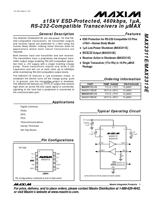
General DescriptionThe MAX3311E/MAX3313E are low-power, 5V EIA/TIA-232-compatible transceivers. All transmitter outputs and receiver inputs are protected to ±15kV using the Human Body Model, making these devices ideal for applications where more robust transceivers are required.Both devices have one transmitter and one receiver.The transmitters have a proprietary low-dropout trans-mitter output stage enabling RS-232-compatible opera-tion from a +5V supply with a single inverting charge pump. These transceivers require only three 0.1µF capacitors and will run at data rates up to 460kbps while maintaining RS-232-compatible output levels.The MAX3311E features a 1µA shutdown mode. In shutdown the device turns off the charge pump, pulls V- to ground, and the transmitter output is disabled.The MAX3313E features an INVALID output that asserts high when an active RS-232 cable signal is connected,signaling to the host that a peripheral is connected to the communication port.________________________ApplicationsDigital Cameras PDAs GPS POSTelecommunications Handy Terminals Set-Top BoxesFeatureso ESD Protection for RS-232-Compatible I/O Pins±15kV—Human Body Modelo 1µA Low-Power Shutdown (MAX3311E)o INVALID Output (MAX3313E)o Receiver Active in Shutdown (MAX3311E)o Single Transceiver (1Tx/1Rx) in 10-Pin µMAX PackageMAX3311E/MAX3313E±15kV ESD-Protected, 460kbps, 1µA,RS-232-Compatible Transceivers in µMAX________________________________________________________________Maxim Integrated Products1Pin Configurations19-1910; Rev 0; 1/01Ordering InformationFor price, delivery, and to place orders,please contact Maxim Distribution at 1-888-629-4642,or visit Maxim’s website at .Typical Operating CircuitM A X 3311E /M A X 3313E±15kV ESD-Protected, 460kbps, 1µA,RS-232-Compatible Transceivers in µMAX 2_______________________________________________________________________________________ABSOLUTE MAXIMUM RATINGSELECTRICAL CHARACTERISTICSStresses beyond those listed under “Absolute Maximum Ratings” may cause permanent damage to the device. These are stress ratings only, and functional operation of the device at these or any other conditions beyond those indicated in the operational sections of the specifications is not implied. Exposure to absolute maximum rating conditions for extended periods may affect device reliability.V CC to GND.............................................................-0.3V to +6V V- to GND................................................................+0.3V to -7V V CC + |V-|............................................................................+13V Input VoltagesTIN, SHDN to GND...............................................-0.3V to +6V RIN to GND......................................................................±25V Output VoltagesTOUT to GND................................................................±13.2V ROUT, INVALID to GND.....................…-0.3V to (V CC + 0.3V)Short-Circuit DurationTOUT to GND.........................................................ContinuousContinuous Power Dissipation10-Pin µMAX (derate 5.6mW/°C above +70°C)..........444mW Operating Temperature RangesMAX331_ECUB.................................................0°C to +70°C MAX331_EEUB..............................................-40°C to +85°C Junction Temperature.....................................................+150°C Storage Temperature Range............................-65°C to +150°C Lead Temperature (soldering, 10s)................................+300°CMAX3311E/MAX3313E±15kV ESD-Protected, 460kbps, 1µA,RS-232-Compatible Transceivers in µMAX_______________________________________________________________________________________3ELECTRICAL CHARACTERISTICS (continued)TIMING CHARACTERISTICSM A X 3311E /M A X 3313E±15kV ESD-Protected, 460kbps, 1µA,RS-232-Compatible Transceivers in µMAX 4_______________________________________________________________________________________Typical Operating Characteristics(V CC = +5V, 0.1µF capacitors, transmitter loaded with 3k Ωand C L , T A = +25°C, unless otherwise noted.)0428612101410001500500200025003000SLEW RATEvs. LOAD CAPACITANCELOAD CAPACITANCE (pF)S L E W R A T E (V /µs )-5-4-3-2-10123456050010001500200025003000TRANSMITTER OUTPUT VOLTAGEvs. LOAD CAPACITANCELOAD CAPACITANCE (pF)T R A N S M I T T E R O U T P U T V O L T A G E (V )010001500500200025003000SUPPLY CURRENT vs. LOAD CAPACITANCELOAD CAPACITANCE (pF)Detailed DescriptionSingle Charge-Pump Voltage ConverterThe MAX3311E/MAX3313E internal power supply has a single inverting charge pump that provides a negative voltage from a single +5V supply. The charge pump operates in a discontinuous mode and requires a flying capacitor (C1) and a reservoir capacitor (C2) to gener-ate the V- supply.RS-232-Compatible DriverThe transmitter is an inverting level translator that con-verts CMOS-logic levels to EIA/TIA-232 compatible lev-els. It guarantees data rates up to 460kbps with worst-case loads of 3k Ωin parallel with 1000pF. When SHDN is driven low, the transmitter is disabled and put into tri-state. The transmitter input does not have an internal pullup resistor.RS-232 ReceiverThe MAX3311E/MAX3313E receiver converts RS-232signals to CMOS-logic output levels. The MAX3311E receiver will remain active during shutdown mode. The MAX3313E INVALID indicates when an RS-232 signal is present at the receiver input, and therefore when the port is in use.The MAX3313E INVALID output is pulled low when no valid RS-232 signal level is detected on the receiver input.MAX3311E Shutdown ModeIn shutdown mode, the charge pump is turned off, V- is pulled to ground, and the transmitter output is disabled (Table 1). This reduces supply current typically to 1µA.The time required to exit shutdown is less than 25ms.Applications InformationCapacitor SelectionThe capacitor type used for C1 and C2 is not critical for proper operation; either polarized or nonpolarized capacitors are acceptable. If polarized capacitors are used, connect polarity as shown in the Typical Operating Circuit . The charge pump requires 0.1µF capacitors. Increasing the capacitor values (e.g., by a factor of 2) reduces power consumption. C2 can beincreased without changing C1’s value. However, do not increase C1’s value without also increasing the value of C2 and C BYPASS to maintain the proper ratios (C1 to the other capacitors).When using the minimum 0.1µF capacitors, make sure the capacitance does not degrade excessively with temperature. If in doubt, use capacitors with a larger nominal value. The capacitor ’s equivalent series resis-tance (ESR) usually rises at low temperatures and influ-ences the amount of ripple on V-.To reduce the output impedance at V-, use larger capacitors (up to 10µF).Bypass V CC to ground with at least 0.1µF. In applica-tions sensitive to power-supply noise generated by the charge pump, decouple V CC to ground with a capaci-tor the same size as (or larger than) charge-pump capacitors C1 and C2.Transmitter Output when ExitingShutdownFigure 1 shows the transmitter output when exiting shutdown mode. The transmitter is loaded with 3k Ωin parallel with 1000pF. The transmitter output displays no ringing or undesirable transients as the MAX3311E comes out of shutdown. Note that the transmitter is enabled only when the magnitude of V- exceeds approximately -3V.High Data RatesThe MAX3311E/MAX3313E maintain RS-232-compati-ble ±3.7V minimum transmitter output voltage even atMAX3311E/MAX3313E±15kV ESD-Protected, 460kbps, 1µA,RS-232-Compatible Transceivers in µMAX5Figure 1. Transmitter Output when Exiting Shutdown or Powering Up10µs/divSHDNTOUT5V/div1.5V/divTIN = GNDTIN = V CCM A X 3311E /M A X 3313E±15kV ESD-Protected, 460kbps, 1µA,RS-232-Compatible Transceivers in µMAX 6_______________________________________________________________________________________high data rates. Figure 2 shows a transmitter loopback test circuit. Figure 3 shows the loopback test result at 120kbps, and Figure 4 shows the same test at 250kbps.±15kV ESD ProtectionAs with all Maxim devices, ESD-protection structures are incorporated on all pins to protect against electro-static discharges encountered during handling and assembly. The MAX3311E/MAX3313E driver outputsand receiver inputs have extra protection against static discharge. Maxim ’s engineers have developed state-of-the-art structures to protect these pins against ESD of ±15kV without damage. The ESD structures withstand high ESD in all states: normal operation, shutdown, and powered down. After an ESD event, Maxim ’s E versions keep working without latchup; whereas, competing products can latch and must be powered down to remove latchup.ESD protection can be tested in various ways. The transmitter outputs and receiver inputs of the product family are characterized for protection to ±15kV using the Human Body Model.ESD Test ConditionsESD performance depends on a variety of conditions.Contact Maxim for a reliability report that documents test setup, test methodology, and test results.Human Body ModelFigure 5 shows the Human Body Model, and Figure 6shows the current waveform it generates when dis-charged into low impedance. This model consists of a 100pF capacitor charged to the ESD voltage of interest,which is then discharged into the test device through a 1.5k Ωresistor.Machine ModelThe Machine Model for ESD tests all pins using a 200pF storage capacitor and zero discharge resis-tance. Its objective is to emulate the stress caused by contact that occurs with handling and assembly during manufacturing. Of course, all pins require this protec-tion during manufacturing, not just RS-232 inputs and outputs. Therefore, after PC board assembly, the Machine Model is less relevant to I/O ports.Figure 4. Loopback Test Results at 250kbps2µs/divTOUTTINROUTFigure 3. Loopback Test Results at 120kbps 5µs/divTOUTTINROUTMAX3311E/MAX3313E±15kV ESD-Protected, 460kbps, 1µA,RS-232-Compatible Transceivers in µMAX_______________________________________________________________________________________7Figure 5. Human Body ESD Test ModelFigure 6. Human Body Current WaveformPin Configurations (continued)Chip InformationTRANSISTOR COUNT: 278M A X 3311E /M A X 3313E±15kV ESD-Protected, 460kbps, 1µA,RS-232-Compatible Transceivers in µMAX Maxim cannot assume responsibility for use of any circuitry other than circuitry entirely embodied in a Maxim product. No circuit patent licenses are implied. Maxim reserves the right to change the circuitry and specifications without notice at any time.8_____________________Maxim Integrated Products, 120 San Gabriel Drive, Sunnyvale, CA 94086 408-737-7600©2001 Maxim Integrated ProductsPrinted USAis a registered trademark of Maxim Integrated Products.______________________________________________________________Pin Description。

General DescriptionThe MAX1932 evaluation kit (EV kit) is a fully assembled and tested surface-mount printed circuit board (PCB).The EV kit contains a MAX1932 step-up switching regu-lator that includes an 8-bit DAC with an SPI™-compati-ble serial interface. The output of the step-up switching regulator is configured for a range of 40V to 90V and can provide up to 2mA. The EV kit is powered from a DC supply providing 4.5V to 5.5V. The EV kit can be reconfigured for an input voltage down to 3V.The SPI-compatible serial interface can be connected to an IBM-compatible PC parallel port for evaluation.Windows ®95/98/2000-compatible software provides a user-friendly interface to demonstrate the features of the MAX1932 IC. The program is menu driven and offers a graphics interface with control buttons.The MAX1932 EV kit features current-limit protection for the output. The MAX1932 thin QFN package and small external components permit the circuit area to be less than 0.6in ✕0.9in.Features♦4.5V to 5.5V Input Range♦Output Voltage Ranges from 40V to 90V♦Output Ranges are Adjustable with Resistors ♦Overcurrent Protection♦SPI-Compatible Serial Interface ♦Menu-Driven Software♦Windows 95/98/2000-Compatible Software ♦Reconfigurable for Input Voltages Down to 3V (Refer to the MAX1932 IC Data Sheet)♦Surface-Mount Components ♦Fully Assembled and TestedEvaluates: MAX1932MAX1932 Evaluation KitOrdering Information19-2650; Rev 1; 4/07For pricing, delivery, and ordering information,please contact Maxim/Dallas Direct!at 1-888-629-4642, or visit Maxim’s website at .SPI is a trademark of Motorola, Inc.Windows is a registered trademark of Microsoft Corp.The MAX1932 IC temperature range is -40°C to +85°C.+Denotes a lead-free and RoHS-compliant EV kit.E v a l u a t e s : M A X 1932Quick StartRequired EquipmentThe following equipment is required:•MAX1932 EV kit•5V, 500mA DC power supply •One voltmeter•(Optional) Windows 95/98/2000 computer with a spare parallel (printer) port •(Optional) 25-pin I/O extension cableProcedure with a ComputerThe MAX1932 EV kit is fully assembled and tested.Follow the steps below to verify board operation.Caution: Do not turn on the power supply until all connections are completed.1)Install shunts on jumpers JU2, JU3, and JU4.2)With the power off, connect the 5V DC power sup-ply to the MAX1932 EV kit.3)Connect the 25-pin I/O extension cable from thecomputer’s parallel port to the MAX1932 EV kit board. The EV kit software uses a loopback con-nection to confirm that the correct port has been selected.4)Install the evaluation software by running theINSTALL.EXE program on the floppy disk. The pro-gram files are copied and icons are created for them in the Windows Start menu.5)Turn on the power supply. Verify that V OUT isapproximately 40V.6)Start the MAX1932 program by opening its icon inthe Start menu.7)Click on SPI 3-Wire Parallel Port Diagnostic (Figure 1).8)Click on Bit-Banging Serial Interface.9)Enter 0x01 into “Data bytes to be written” and clickon Send Now (Figure 2).10)Verify that the voltage at the VOUT pad is approxi-mately 90V.11)Enter 0xFF into the “Data bytes to be written” boxand click on Send Now.12)Verify that the voltage at the VOUT pad is approxi-mately 40V.13)Header J2 is provided to monitor the parallel portpins supplying the CLK _P, CS_P, DIN_P (5V sig-nals), and loopback signal. The CS, SCLK, and DIN pads on the EV kit’s bottom edge are V CC level-shifted signals from the MAX1841 translator. Both signal locations can be used for monitoring.For instructions on selecting the feedback resistors for other output voltages, see the Output Voltage Range section.Procedure without a ComputerDo not turn on the power supply until all connections are completed:1)Remove shunts on jumpers JU2, JU3, and JU4.2)With the power off, connect the 5V DC power sup-ply to the MAX1932 EV kit.3)Turn on the power supply. Verify that V OUT isapproximately 40V.MAX1932 Evaluation Kit 2_______________________________________________________________________________________Figure 1. MAX1932 Evaluation Software’s Main Window to Access the SPI 3-Wire Parallel Port Diagnostic UtilityDetailed DescriptionThe MAX1932 EV kit contains a step-up switching regu-lator that includes an 8-bit DAC with an SPI-compatible serial interface. The output of the EV kit has two set-tings: the range voltage setting and a specific voltage setting within the range.As configured, the step-up switching regulator can generate an output range of 40V to 90V and provide up to 2mA of current to the output with 4.75V input. The step-up switching-regulator output voltage can be reconfigured to ranges of 4.5V to 15V, 4.5V to 45V, and 20V to 60V with proper resistor selection (see the Output Voltage Range section).The voltage setting within the range is set by the 8-bit DAC that receives input data from the SPI-compatible interface. The EV kit connects to a compatible PC par-allel port and uses the port to control the EV kit. The EV kit’s SPI signals are connected to a MAX1841 level translator (U2). The translator level shifts the comput-er’s parallel port logic 5V signals to the EV kit’s logic VCC voltage level chosen by the user. The translator can function with voltages down to 2.7V. The leveltranslator’s parallel port side is powered by the parallel port’s data pins 6, 7, 8, and 9, diodes D2/D3, and capac-itor C6, which provides approximately 5V to the transla-tor’s input. The power supply connected to V CC provides power to the level translator’s output. A 5-pin header (J2) is provided for monitoring the 5V CLK _P,CS_P, DIN_P nonlevel-translated and loopback signals coming from the parallel port cable.The EV kit can be reconfigured for stand-alone opera-tion and connected to an external microcontroller for evaluation. PCB pads are provided for interfacing or monitoring the CS , SCLK, and DIN level-translated pins of the MAX1932 IC.Output Voltage RangeStep-Up Switching RegulatorOutput RangeThe MAX1932 EV kit’s step-up switching regulator output range is set from 40V to 90V by feedback resistors R5,R6, and R8. To generate output voltage ranges other than 40V to 90V (4.5V to 15V, 4.5V to 45V, or 20V to 60V), select different external voltage-divider resistors (R5, R6, and R8). Refer to the Output and DAC Adjustment Range section in the MAX1932 data sheet for instruction on selecting resistors.Jumper SelectionStand-Alone ConfigurationThe MAX1932 EV kit features four jumpers (JU1–JU4)to reconfigure the EV kit for stand-alone operation mode or PC/software control mode. Tables 1 and 2 list the options for the desired evaluation mode. Note:All jumpers must be configured for only one mode at a time. A suitable voltage must be selected for stand-alone mode. Configure all jumpers for either stand-alone or PC/software control mode.Detailed Descriptionof SoftwareThe MAX1932 EV kit software’s main window has a but-ton to start the SPI 3-wire parallel port diagnostic utility used for bit-banging data into the MAX1932. Click on SPI 3-Wire Parallel Port Diagnostic to start the utility.SPI/3-Wire DiagnosticThe SPI/3-wire diagnostic screen allows you to send SPI or 3-wire commands, or manipulate the parallel port pins directly. Each of the 25 pins is represented by a checkbox. A checkmark means that the corresponding pin is at a logic-high level. Unused and grounded pins are gray.Evaluates: MAX1932MAX1932 Evaluation Kit_______________________________________________________________________________________________________3Figure 2. Parallel Port Diagnostic Window’s Bit-Banging Serial Interface TabE v a l u a t e s : M A X 1932The bit-banging SPI diagnostic utility transmits data using synchronous serial format (similar to Motorola’s 68HC11 SPI interface). The SPI interface sends and receives data simultaneously on separate pins. Parallel port pin 2 drives the CLK_P, pin 3 drives CS_P, and pin 4 drives DIN_P.The data to be sent is 8-bit data represented by a two-digit hexadecimal DAC code. The DAC code ranges from 0x01 to 0xFF. The output is at the higher limit, 90V,when the DAC code is 0x01, and at the lower limit, 40V,when the DAC code is 0xFF. The DAC code is entered in the “Data bytes to be written” box and transmitted by clicking on Send Now.TroubleshootingProblem: Cannot find the MAX1932 EV kit parallel port connection.Ensure that the I/O extension cable is connected to a parallel port and not to a SCSI or other type of port.Verify that the supplied LPTCON.VXD is in the same directory as MAX1932.EXE. If a local printer driver is installed, temporarily disable it. The software does not work if the program icon is dragged onto the Windows desktop.MAX1932 Evaluation Kit 4_______________________________________________________________________________________Evaluates: MAX1932MAX1932 Evaluation Kit_______________________________________________________________________________________5Figure 3a. MAX1932 EV Kit Schematic (Sheet 1 of 2)E v a l u a t e s : M A X 1932MAX1932 Evaluation Kit 6_______________________________________________________________________________________Figure 3b. MAX1932 EV Kit Schematic (Sheet 2 of 2)Evaluates: MAX1932MAX1932 Evaluation Kit_______________________________________________________________________________________7Figure 4. MAX1932 EV Kit Component Placement Guide—Component Side Figure 5. MAX1932 EV Kit Component Placement Guide—Solder SideE v a l u a t e s : M A X 1932MAX1932 Evaluation Kit M axim cannot assume responsibility for use of any circuitry other than circuitry entirely embodied in a M axim product. No circuit patent licenses are implied. Maxim reserves the right to change the circuitry and specifications without notice at any time.8_____________________Maxim Integrated Products, 120 San Gabriel Drive, Sunnyvale, CA 94086 408-737-7600©2007 Maxim Integrated Productsis a registered trademark of Maxim Integrated Products, Inc.Figure 6. MAX1932 EV Kit PCB Layout—Component SideFigure 7. MAX1932 EV Kit PCB Layout—Solder SideRevision HistoryPages changed at Rev 1: 1, 2, 3, 5, 6, 7。

AG9311带PD3.0 Type C转HDMI转换器AG9311AG9311Type-C转HDMI转换器数据表修订历史PS:本中文规格书由第三方翻译软件自动翻译,权威信息请以原厂英文版规格书为准。
2AG9311Type-C转HDMI转换器数据表索引1.概述 (5)2.特性 (5)3.设备信息 (6)4.应用 (6)5.系统框图 (7)6.管脚映射和描述 (8)7.规格明细 (15)i. 绝对最大额定值绝对最大额定值 (15)ii. 直流特性/工作条件 (15)iii. 交流特性 (16)8. 包装和标记规范 (19)3AG9311Type-C转HDMI转换器数据表图目录图1 Type-C转HDMI 适配器的应用 (6)图2系统框图 (7)图3 AG9311MAQ引脚映射 (8)图4 AG9311-MCQ引脚映射 (12)图5 AG9311-MAQ包装尺寸..... (20)图6 AG9311-MCQ包装尺寸 (21)表格列表表1引脚说明........ (9)表2引脚说明....... (12)表3绝对最大额定值 (15)表4数字I/O规范.... (16)表5显示端口输入 (16)表6显示端口辅助通道I/O规格. (17)表7 USB I/O规格 (18)表8 USB PD规格 (18)4AG9311Type-C转HDMI转换器数据表一、概述ALGOLTEK AG9311是一款高度集成的解决方案,通过USB Type-C将视频和音频从DisplayPort alternate mode传输到HDMI输出。
AG9311支持各种@1.62Gbps、2.7Gbps和5.4Gbpsup通到DisplayPort 1.2,支持1路2路通道;HDMI支持4K/2K@30Hz输出。
用户可以轻松地将AG9311集成到视频转换适配器和扩展坞上。
二、特性1、显示符合 DisplayPort specification Revision 1.2支持1.62(RBR)/2.7(HBR)/5.4(HBR2)Gbps数据速率支持1/2线路配置支持下行扩频时钟(SSC)-支持I2S总线音频提取2、HDMIHDMI 高清多媒体接口符合HDMI1.4和HDCP1.4规范支持高达3Gbps的TMD支持分辨率高达4kx2k@30Hz输出支持HDCP键预先编程兼容EDID和MCCS支持采样率48kHz/44.1KHz/32KHz的LPCM双通道3、USB Type-C PD支持显示端口备用模式协议DisplayPort Alternate符合USB PD3.0集成Type-C RP and RD电阻器支持2个 USB Type-C端口支持USB宣称集成USB2.0全速5AG9311Type-C转HDMI转换器数据表4、单片机系统及接口集成16位单片机集成用于固件升级的64KB闪存支持I2C主/从、UART、USB2.0全速支持3通道8 bit分辨率ADC5、电源操作和ESD3.3V:3V至3.6V操作1.2V:1.08至1.32V运行1.2V核心电源和3.3V I/O电源HBM 2KV ESD性能三、设备信息四、应用USB Type-C 转换器USB Type-C扩展坞6AG9311Type-C转HDMI转换器数据表五、系统框图7AG9311Type-C转HDMI转换器数据表六、管脚映射和描述图3 AG9311-MAQ引脚映射8AG9311Type-C转HDMI转换器数据表表1基本说明9AG9311Type-C转HDMI转换器数据表10AG9311Type-C转HDMI转换器数据表11AG9311Type-C转HDMI转换器数据表图4 AG9311-MCQ引脚映射表2引脚说明12AG9311 Type-C转HDMI转换器数据表13AG9311 Type-C转HDMI转换器数据表14AG9311Type-C转HDMI转换器数据表七、规格明细1.绝对最大额定值表3绝对最大额定值2.直流特性/工作条件15AG9311Type-C转HDMI转换器数据表Table 4 Digital I/O Specification表4数字I/O规范3.交流特性显示端口主链交流特性表5显示端口输入定时16AG9311Type-C转HDMI转换器数据表显示端口AUX-CH AC特性表6显示端口辅助通道I/O规格17AG9311Type-C转HDMI转换器数据表USB PD BMC接收器规范要求表7 USB I/O规格USB PD BMC发射机规范要求表8 USB PD规格AG9311Type-C转HDMI转换器数据表八、包装和标记规范标记19AG9311Type-C转HDMI转换器数据表包装尺寸AG9311-MAQ: QFN-64L 8x8mm(E-PAD SIZE:181x18*MIL)图5 AG9311-MAQ包装尺寸20AG9311Type-C转HDMI转换器数据表AG9311-MCQ:QFN-48L 6x6mm(电子板尺寸:185x18*MIL)Figure 6 AG9311-MCQ Package Dimension图6 AG9311-MCQ包装尺寸21。


AG9311USB Type-C to HDMI with Power Delivery 3.0ConverterData SheetOfficial VersionV1.6July, 2018Revision HistoryIndexI. General Description (5)II. Features (5)III. Device Information (6)IV. Application (6)V. System Block Diagram (7)VI. Pin Mapping and Description (8)VII. Specification (15)i. Absolute Maximum Rating (15)ii. DC Characteristics/Operating Conditions (15)iii. AC Characteristics (16)VIII. Packing and Marking Specification (19)IX. References (22)X. (22)List of FigureFigure 1 Application for Type-C to HDMI Dongle (6)Figure 2 System Block Diagram (7)Figure 3 AG9311-MAQ Pin Mapping (8)Figure 4 AG9311-MCQ Pin Mapping (12)Figure 5 AG9311-MAQ Package Dimension (20)Figure 6 AG9311-MCQ Package Dimension (21)List of TableTable 1 PIN Description (9)Table 2 PIN Description (12)Table 3 Absolute Maximum Rating (15)Table 4 Digital I/O Specification (16)Table 5 DisplayPort Input Timing (16)Table 6 DisplayPort AUX Channel I/O Specification (17)Table 7 USB I/O Specification (18)Table 8 USB PD Specification (18)I.General DescriptionALGOL TEK AG9311 is highly integration solution transmit video and audio stream from DP alternate mode over USB Type-C to HDMI output. The AG9311 provides DisplayPort 1.2 receiver over various @1.62Gbps, 2.7Gbps and 5.4Gbps up to 2 lanes; and supports HDMI frequencies up to 297MHz, which enables 4K x 2K@30Hz. User easily integrate AG9311 on any USB Type-C video conversion on dongles and docking stations application.II.Features●DisplayPort-Compliant to DisplayPort specification Revision 1.2-Support 1.62(RBR)/2.7(HBR)/5.4(HBR2) Gbps data rate-Support 1/2 Lane configurations-Down Spread Spectrum Clock (SSC) supported-Support Audio Extraction over I2S bus●HDMI-Compliant to HDMI1.4 and HDCP1.4 specifications-Support TMDS up to 3Gbps-Support resolution up to 4K x 2K @30Hz output-Pre-programmed with HDCP key-Transparent EDID and MCCS-Support LPCM 2-Channel of sample rate 48kHz/44.1KHz/32KHz●USB Type-C and Power Delivery-Support DisplayPort Alternate mode protocol-Compliant to USB Power Delivery specification Revision 3.0-Integrated complete termination of the Type-C R P and R D resistors-Supports two USB Type-C port-Support USB Billboard function-Integrated USB2.0 Full-speed PHY●MCU System and Interface-Embedded 16 bit MCU on-chip-Embedded 64KB flash for firmware upgrade-Support I2C Master/Slave, UART and USB2.0 Full-speed-Support 3-Channel ADC-8bit resolutions●Power Operation and ESD-3.3V: 3V to 3.6V operation-1.2V: 1.08 to 1.32V operation-1.2V Core power and 3.3V I/O power-HBM 2KV ESD performanceAG9311Figure 1 Application for Type-C to HDMI DongleV.System Block DiagramVI.Pin Mapping and DescriptionFigure 3 AG9311-MAQ Pin MappingTable PIN DescriptionVII.Specificationi.Absolute Maximum RatingTable 4 Digital I/O Specification iii.AC CharacteristicsTable 5 DisplayPort Input TimingVIII.Packing and Marking Specification MarkingAGX1X2X3X4 - X5X6L4L5L6L7L8L9L10L112P3P4P5P6P7P8PPackage DimensionAG9311-MAQ: QFN-64L 8x8mm(E-PAD SIZE:181x18*MIL)Figure 5 AG9311-MAQ Package DimensionAG9311-MCQ: QFN-48L 6x6mm(E-PAD SIZE:185x18*MIL)Figure 6 AG9311-MCQ Package DimensionIX.References●DisplayPort TM Standard 1.2b Specification●HDMI 1.4b SpecificationX.Contact InformationTrademark AcknowledgementsThe company and product names mentioned in this document may be the trademarks or registered trademarks of their manufactures.DisclaimerAlgoltek, Inc. reserves the right to change this product without prior notice.Algoltek, Inc. makes no warranty for the use of its products and bears no responsibility for any error that appear in this document. Specifications are subject to change without prior notice.。

General DescriptionThe MAX9311/MAX9313 are low-skew, 1-to-10 differen-tial drivers designed for clock and data distribution.These devices allow selection between two inputs. The selected input is reproduced at 10 differential outputs.The differential inputs can be adapted to accept single-ended inputs by connecting the on-chip V BB supply to one input as a reference voltage.The MAX9311/MAX9313 feature low part-to-part skew (30ps) and output-to-output skew (12ps), making them ideal for clock and data distribution across a backplane or a board. For interfacing to differential H STL and LVPECL signals, these devices operate over a +2.25V to +3.8V supply range, allowing high-performance clock or data distribution in systems with a nominal +2.5V or +3.3V supply. For differential LVECL operation, these devices operate from a -2.25V to -3.8V supply.The MAX9311 features an on-chip V BB reference output of 1.425V below the positive supply voltage. The MAX9313 offers an on-chip V BB reference output of 1.32V below the positive supply voltage.Both devices are offered in space-saving, 32-pin 5mm ✕5mm TQFP, 5mm x 5mm QFN, and industry-standard 32-pin 7mm x 7mm LQFP packages.ApplicationsPrecision Clock Distribution Low-Jitter Data RepeaterFeatureso +2.25V to +3.8V Differential HSTL/LVPECL Operation o -2.25V to -3.8V LVECL Operation o 30ps (typ) Part-to-Part Skew o 12ps (typ) Output-to-Output Skew o 312ps (typ) Propagation Delay o ≥300mV Differential Output at 3GHz o On-Chip Reference for Single-Ended Inputs o Output Low with Open Inputo Pin Compatible with MC100LVEP111 (MAX9311)and MC100EP111 (MAX9313)o Offered in Tiny QFN* Package (70% Smaller Footprint than LQFP)MAX9311/MAX93131:10 Differential LVPECL/LVECL/HSTLClock and Data Drivers________________________________________________________________Maxim Integrated Products 1Pin ConfigurationOrdering Information19-2078; Rev 2; 10/02For pricing, delivery, and ordering information,please contact Maxim/Dallas Direct!at 1-888-629-4642, or visit Maxim’s website at .*Future product—contact factory for availability.M A X 9311/M A X 93131:10 Differential LVPECL/LVECL/HSTL Clock and Data Drivers 2_______________________________________________________________________________________ABSOLUTE MAXIMUM RATINGSDC ELECTRICAL CHARACTERISTICSStresses beyond those listed under “Absolute Maximum Ratings” may cause permanent damage to the device. These are stress ratings only, and functional operation of the device at these or any other conditions beyond those indicated in the operational sections of the specifications is not implied. Exposure to absolute maximum rating conditions for extended periods may affect device reliability.V CC - V EE ...............................................................................4.1V Inputs (CLK_, CLK_, CLKSEL)..............V EE - 0.3V to V CC + 0.3V CLK_ to CLK_....................................................................±3.0V Continuous Output Current.................................................50mA Surge Output Current........................................................100mA V BB Sink/Source Current...............................................±0.65mA Junction-to-Ambient Thermal Resistance in Still Air7mm x 7mm LQFP.....................................................+90°C/W Junction-to-Ambient Thermal Resistance with 500 LFPM Airflow7mm x 7mm LQFP.....................................................+60°C/WJunction-to-Case Thermal Resistance7mm x 7mm LQFP.....................................................+12°C/W Operating Temperature Range ...........................-40°C to +85°C Junction Temperature......................................................+150°C Storage Temperature Range.............................-65°C to +150°C ESD ProtectionHuman Body Model (CLKSEL, CLK_, CLK_,Q_, Q_,V BB ).......................................................................2kV Soldering Temperature (10s)...........................................+300°CMAX9311/MAX93131:10 Differential LVPECL/LVECL/HSTLClock and Data Drivers_______________________________________________________________________________________3DC ELECTRICAL CHARACTERISTICS (continued)(V CC - V EE = +2.25V to +3.8V, outputs loaded with 50Ω±1% to V CC - 2V, CLKSEL = high or low, unless otherwise noted.) (Notes 1–4)M A X 9311/M A X 93131:10 Differential LVPECL/LVECL/HSTL Clock and Data Drivers 4_______________________________________________________________________________________AC ELECTRICAL CHARACTERISTICS(V CC - V EE = 2.25V to 3.8V, outputs loaded with 50Ω±1% to V CC - 2V, input frequency = 1.5GH z, input transition time = 125ps (20% to 80%), CLKSEL = high or low, V IHD = V EE + 1.2V to V CC , V ILD = V EE to V CC - 0.15V, V IHD - V ILD = 0.15V to the smaller of 3V or V CC - V EE , unless otherwise noted. Typical values are at V CC - V EE = 3.3V, V IHD = V CC -1V, V ILD = V CC -1.5V.) (Note 7)Note 3:Single-ended input operation using V BB is limited to V CC - V EE = 3.0V to 3.8V for the MAX9311 and V CC - V EE = 2.7V to 3.8Vfor the MAX9313.Note 4:DC parameters production tested at T A = +25°C. Guaranteed by design and characterization over the full operating temper-ature range.Note 5:Use V BB only for inputs that are on the same device as the V BB reference.Note 6:All pins open except V CC and V EE .Note 7:Guaranteed by design and characterization. Limits are set at ±6 sigma.Note 8:Measured between outputs of the same part at the signal crossing points for a same-edge transition.Note 9:Measured between outputs of different parts at the signal crossing points under identical conditions for a same-edgetransition.Note 10:Device jitter added to the input signal.MAX9311/MAX93131:10 Differential LVPECL/LVECL/HSTLClock and Data Drivers_______________________________________________________________________________________5Typical Operating Characteristics(V CC = +3.3V, V EE = 0, V IHD = V CC - 0.95V, V ILD = V CC - 1.25V, input transition time = 125ps (20% to 80%), f IN = 1.5GHz, outputs loaded with 50Ωto V CC - 2V, T A = +25°C, unless otherwise noted.)5060557065807585-4010-15356085SUPPLY CURRENT (I EE )vs. TEMPERATUREM A X 9311 t o c 01TEMPERATURE (°C)S U P P L Y C U R R E N T (m A )0.20.30.40.50.60.70.80.90100020003000OUTPUT AMPLITUDE (V OH - V OL )vs. FREQUENCYM A X 9311 t o c 02FREQUENCY (MHz)O U T P U T A M P L I T U D E (V )0.1100130-40-1510356085TRANSITION TIME vs. TEMPERATURETEMPERATURE (°C)T R A N S I T I O N T I M E (p s )1051101151201253033053043073063093083103123113131.03.8PROPAGATION DELAY vs. HIGH VOLTAGE OF DIFFERENTIAL INPUT (V IHD )V IHD (V)P R O P A G A T I O N D E L A Y (p s )1.41.82.23.43.02.6200220240260280300320340360-40-1510356085PROPAGATION DELAY vs. TEMPERATURETEMPERATURE (°C)P R O P A G A T I O N D E L A Y (p s )M A X 9311/M A X 93131:10 Differential LVPECL/LVECL/HSTL Clock and Data Drivers 6_______________________________________________________________________________________MAX9311/MAX93131:10 Differential LVPECL/LVECL/HSTLClock and Data Drivers_______________________________________________________________________________________7Detailed DescriptionThe MAX9311/MAX9313 are low skew, 1-to-10 differen-tial drivers designed for clock and data distribution.A 2:1 mux selects between the two differential inputs,CLK0, CLK0and CLK1, CLK1. The 2:1 mux is switched by the single-ended CLKSEL input. A logic low selects the CLK0, CLK0input. A logic high selects the CLK1,CLK1input. The logic threshold for CLKSEL is set by an internal V BB voltage reference. The CLKSEL input can be driven to V CC and V EE or by a single-ended LVPECL/LVECL signal. The selected input is reproduced at 10differential outputs.For interfacing to differential HSTL and LVPECL signals,these devices operate over a +2.25V to +3.8V supply range, allowing high-performance clock or data distribu-tion in systems with a nominal +2.5V or +3.3V supply.For differential LVECL operation, these devices operate from a -2.25V to -3.8V supply.The differential inputs can be configured to accept sin-gle-ended inputs when operating at approximately V CC -V EE = +3.0V to +3.8V for the MAX9311 or V CC - V EE =+2.7V to +3.8V for the MAX9313. This is accomplished by connecting the on-chip reference voltage, V BB , to an input as a reference. For example, the differential CLK0,CLK0input is converted to a noninverting, single-ended input by connecting V BB to CLK0and connecting the single-ended input to CLK0. Similarly, an inverting input is obtained by connecting V BB to CLK0 and connecting the single-ended input to CLK0. With a differential input configured as single-ended (using V BB ), the single-ended input can be driven to V CC and V EE or with a sin-gle-ended LVPECL/LVECL signal.When a differential input is configured as a single-ended input (using V BB ), the approximate supply range is V CC -V EE = +3.0V to +3.8V for the MAX9311 and V CC - V EE =+2.7V to +3.8V for the MAX9313. This is because one of the inputs must be V EE + 1.2V or higher for proper oper-ation of the input stage. V BB must be at least V EE + 1.2V because it becomes the high-level input when the other (single-ended) input swings below it. Therefore, mini-mum V BB = V EE + 1.2V.The minimum V BB output for the MAX9311 is V CC -1.525V and the minimum V BB output for the MAX9313 is V CC - 1.38V. Substituting the minimum V BB output for each device into V BB = V EE + 1.2V results in a minimum supply of 2.725V for the MAX9311 and 2.58V for the MAX9313. Rounding up to standard supplies gives the single-ended operating supply ranges of V CC - V EE =3.0V to 3.8V for the MAX9311 and V CC - V EE = 2.7V to 3.8V for the MAX9313.When using the V BB reference output, bypass it with a 0.01µF ceramic capacitor to V CC . If the V BB reference is not used, it can be left open. The V BB reference can source or sink 0.5mA, which is sufficient to drive two inputs. Use V BB only for inputs that are on the same device as the V BB reference.The maximum magnitude of the differential input from CLK_ to CLK_is 3.0V or V CC - V EE , whichever is less.This limit also applies to the difference between any ref-erence voltage input and a single-ended input.The differential inputs have bias resistors that drive the outputs to a differential low when the inputs are open.The inverting inputs (CLK0and CLK1) are biased with a 75k Ωpullup to V CC and a 75k Ωpulldown to V EE . The noninverting inputs (CLK0 and CLK1) are biased with a 75k Ωpulldown to V EE . The single-ended CLKSEL input does not have a bias resistor. If not driven, pull CLKSEL up or down with a 1kHz resistor (see Pin Description ).Specifications for the high and low voltages of a differen-tial input (V IHD and V ILD ) and the differential input volt-age (V IHD - V ILD ) apply simultaneously (V ILD cannot be higher than V IHD ).Output levels are referenced to V CC and are considered LVPECL or LVECL, depending on the level of the V CC supply. With V CC connected to a positive supply and V EE connected to GND, the outputs are LVPECL. The outputs are LVECL when V CC is connected to GND and V EE is connected to a negative supply.A single-ended input of at least V BB ±95mV or a differen-tial input of at least 95mV switches the outputs to the V OH and V OL levels specified in the DC Electrical Characteristics table.Applications InformationSupply BypassingBypass V CC to V EE with high-frequency surface-mount ceramic 0.1µF and 0.01µF capacitors in parallel as close to the device as possible, with the 0.01µF value capaci-tor closest to the device. Use multiple parallel vias for low inductance. When using the V BB reference output,bypass it with a 0.01µF ceramic capacitor to V CC (if the V BB reference is not used, it can be left open).TracesInput and output trace characteristics affect the perfor-mance of the MAX9311/MAX9313. Connect each signal of a differential input or output to a 50Ωcharacteristic impedance trace. Minimize the number of vias to prevent impedance discontinuities. Reduce reflections by main-taining the 50Ωcharacteristic impedance through con-nectors and across cables. Reduce skew within aM A X 9311/M A X 93131:10 Differential LVPECL/LVECL/HSTL Clock and Data Drivers8_______________________________________________________________________________________differential pair by matching the electrical length of the traces.Output TerminationTerminate outputs through 50Ωto V CC - 2V or use an equivalent Thevenin termination. When a single-ended signal is taken from a differential output, terminate both outputs. For example, if Q0 is used as a single-ended output, terminate both Q0 and Q0.Chip InformationTRANSISTOR COUNT: 250Figure 1. Switching with Single-Ended InputFigure 2. Differential Transition Time and Propagation Delay Timing DiagramMAX9311/MAX93131:10 Differential LVPECL/LVECL/HSTLClock and Data Drivers_______________________________________________________________________________________9Functional DiagramM A X 9311/M A X 93131:10 Differential LVPECL/LVECL/HSTL Clock and Data Drivers 10______________________________________________________________________________________Package Information(The package drawing(s) in this data sheet may not reflect the most current specifications. For the latest package outline information go to /packages .)MAX9311/MAX93131:10 Differential LVPECL/LVECL/HSTL Clock and Data Drivers______________________________________________________________________________________11Package Information (continued)(The package drawing(s) in this data sheet may not reflect the most current specifications. For the latest package outline information go to /packages .)M A X 9311/M A X 93131:10 Differential LVPECL/LVECL/HSTL Clock and Data DriversMaxim cannot assume responsibility for use of any circuitry other than circuitry entirely embodied in a Maxim product. No circuit patent licenses are implied. Maxim reserves the right to change the circuitry and specifications without notice at any time.12____________________Maxim Integrated Products, 120 San Gabriel Drive, Sunnyvale, CA 94086 408-737-7600©2002 Maxim Integrated Products Printed USA is a registered trademark of Maxim Integrated Products.Package Information (continued)(The package drawing(s) in this data sheet may not reflect the most current specifications. For the latest package outline information go to /packages .)。