Simulation of Microstructure Evolution
- 格式:pdf
- 大小:2.63 MB
- 文档页数:35

多尺度铝合金变形组织演变建模研究进展1王冠1,2,卞东伟1,寇琳媛1,易杰2,刘志文2,李落星2(1.宁夏大学机械工程学院,银川750021;2.湖南大学,汽车车身先进设计制造国家重点实验室,长沙410082;)摘要:铝合金在热成型过程中,微观组织会发生晶粒长大、晶粒不均匀变形、动态再结晶等一系列复杂的演化,而这些材料内部微观结构的改变,会直接影响到铝合金的综合性能。
通过掌握变形过程中微观组织演变的物理本质,来达到控制微观组织及产品性能的目的,已经越来越受到材料研究者的重视。
本文综述了铝合金变形组织演变建模的研究现状,重点介绍了多尺度模拟方法,同时指出了研究中存在的问题,展望了铝合金变形组织演变建模的发展趋势。
关键词:铝合金;微观组织演变;多尺度建模;热压缩变形;Research Progress in Multi-scale modelling of microstructure evolution during hot deformation ofaluminum alloyWANG Guan1,2, BIAN Dong-wei1, KOU Lin-yuan1, YI Jie2, LIU Zhi-wen2, LI Luo-xing2(1.College of Mechanical Engineering, Ningxia University, Yinchuan 750021, China;2.State Key Laboratory of Advanced Design and Manufacture for Vehicle body, Hunan University,Changsha 410082;)Abstract:During the hot forming process of aluminum alloy, microstructure will occur in a series of complex evolution such as grain growth, inhomogeneous deformation, dynamic recrystallization and which will directly affect the comprehensive properties of aluminum alloy. By mastering the physical essence of the microstructure evolution during heat deformation, to achieve the purpose of controlling the microstructure and the properties of the products has been paid more and more attention by the researchers of materials. This paper summarizes the research status quo of modelling of microstructure evolution during hot deformation of aluminum alloy, especially for the multi-scale simulation method, and points out the problems existing in current research and forecast the development trend of modelling of microstructure evolution during hot deformation of aluminum alloy.Key words: Aluminum alloy; Microstructure evolution; Multi-scale modelling; Hot compression deformation;铝合金具有密度低、比强度高、耐腐蚀性好、可循环利用等优点,被公认为汽车轻量化的理想材料。


第42卷第7期2015年7月Vol.42,No.7July,2015中国激光CHINESE JOURNAL OF LASERS 超高应变率力学效应下多晶铜的微观塑性变形分子动力学模拟王志龙罗开玉刘月鲁金忠江苏大学机械工程学院,江苏镇江212013摘要激光冲击强化利用离子体力学效应在金属表面形成较深的残余压应力层,细化表层晶粒,大幅度提高金属抗疲劳、抗磨损和抗腐蚀等机械性能。
目前现有实验手段很难获取超高应变速率下塑性变形过程中微观结构演变的动态过程。
本文采用LAMMPS 软件对在2×10⁷s -1应变率,15ns 的加载时间,300K 温度下的多晶铜塑性变形行为进行分子动力学模拟,获得超高应变速率力学效应下多晶铜塑性变形微观结构的演变过程。
超高应变率下力学效应作用下,形变孪晶是中层错能金属亚微米晶粒细化的主要变形方式。
关键词激光技术;超高应变率;力学效应;塑性变形;分子动力学;多晶铜中图分类号TN249文献标识码Adoi:10.3788/CJL201542.0703005Molecular Dynamics Simulation of Plastic Deformation ofPolycrystalline Cu under Mechanical Effect with Ultrahigh Strain RateWang Zhilong Luo Kaiyu Liu Yue Lu JinzhongSchool of Mechanical Engineering,Jiangsu University,Zhenjiang,Jiangsu 212013,ChinaAbstract Laser shock processing utilizes mechanical effect with ultrahigh strain rate to generate deeper residualcompressive stress and grain refinement layer,which improves mechanical properties,such as fatigue resistance,wear resistance and corrosion resistance.To date,it is very difficult to present dynamic microstructure evolutionat ultra-short time (several ten nanoseconds)during the plastic deformation at ultrahigh strain rate usingexperimental method.At temperature of 300K,a molecular dynamics of polycrystalline Cu with a loading durationof 15ns at a strain rate of 2×10⁷s -1is conducted to describe the microstructure evolution process with the LAMMPSsoft.Under the mechanical effect of laser shock wave with a ultra-high strain rate,deformation twinning is theimportant microstructure of grain refinement of the alloys with medium stacking fault energy.Key words laser technique;ultrahigh strain rate;mechanical effect;plastic deformation;molecular dynamics;polycrystalline CuOCIS codes 350.3390;310.4925;120.6660收稿日期:2015-01-16;收到修改稿日期:2015-04-07基金项目:国家自然科学基金(51275220)、江苏省杰出青年基金项目(BK20140012)、江苏省“六大人才高峰”高层次人才项目(2014-ZBZZ-015)、江苏省高校自然科学研究重大项目(14KJA460002)、江苏省高校“青蓝工程”骨干教师计划等作者简介:王志龙(1989—),硕士研究生,主要从事激光表面改性技术方面的研究。
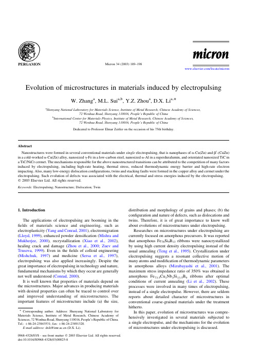
Evolution of microstructures in materials induced by electropulsingW.Zhang a ,M.L.Sui a,b ,Y.Z.Zhou a ,D.X.Li a,*aShenyang National Laboratory for Materials Science,Institute of Metal Research,Chinese Academy of Sciences,72Wenhua Road,Shenyang 110016,People’s Republic of ChinabInternational Center for Materials Physics,Institute of Metal Research,Chinese Academy of Sciences,72Wenhua Road,Shenyang 110016,People’s Republic of ChinaDedicated to Professor Elmar Zeitler on the occasion of his 75th birthday.AbstractNanostructures were formed in several conventional materials under single electropulsing,that is nanophases of a -Cu(Zn)and b 0-(CuZn)in a cold-worked a -Cu(Zn)alloy,nanosized g -Fe in a low-carbon steel,nanosized a -Al in a superduralumin,and orientated nanosized TiC in a TiC/NiCr cermet.The mechanisms responsible for the above nanostructured transitions can be attributed to the competition of many factors induced by electropulsing,including high-rate heating,thermal stress,reduced thermodynamic energy barrier and high-rate electron impacting.Also,many low-energy dislocation configurations,twins and stacking faults were formed in the copper alloy and cermet under the electropulsing.Such evolution of defects was associated with the electrical,thermal and stress energies induced by the electropulsing.q 2003Elsevier Ltd.All rights reserved.Keywords:Electropulsing;Nanostructure;Dislocation;Twin1.IntroductionThe applications of electropulsing are booming in the fields of materials science and engineering,such as electroplasticity (Yang and Conrad,2001),electromigration (Lloyd,1999),enhanced powder densification (Mishra and Mukherjee,2000),recrystallization (Xiao et al.,2002),healing crack and damage (Zhou et al.,2000;Zuev and Trusova,1999).Even in the fields of colloid engineering (Mishchuk,1997)and medicine (Sersa et al.,1997),electropulsing was also applied increasingly.Despite the great importance of electropulsing in technology and nature,fundamental mechanisms by which they occur are generally not well understood (Conrad,2000).It is well known that properties of materials depend on the microstructures.Major advances in producing materials with desired properties can often be traced to control over and improved understanding of microstructures.The important features of microstructure include (a)the size,distribution and morphology of grains and phases;(b)the configuration and nature of defects,such as dislocations and twins.Therefore,it is of great importance to know well about evolutions of microstructures under electropulsing.Researches on microstructures under electropulsing are currently focused on amorphous precursors.It was reported that amorphous Fe 78Si 9B 13ribbons were nanocrystallized by using high current density electropulsing instead of the usual annealing (Teng et al.,1995).Crystallization under electropulsing suggests a resonant collective motion of many atoms and modification of thermodynamic parameters in amorphous alloys (Mizubayashi et al.,2001).The maximum stress impedance ratio of 350%was obtained in amorphous Fe 73.5Cu 1Nb 3Si 13.5B 9ribbons after optimal conditions of current annealing (Li et al.,2002).These processes were involved in many times of electropulsing,instead of a single electropulse.However,there are seldom reports about detailed character of microstructures in conventional coarse-grained materials under the treatment hitherto.In this paper,evolution of microstructures was compre-hensively investigated in several materials subjected to a single electropulse,and the mechanisms for the evolution of microstructures under electropulsing is discussed.0968-4328/03/$-see front matter q 2003Elsevier Ltd.All rights reserved.doi:10.1016/S0968-4328(03)00025-8Micron 34(2003)189–198/locate/micron*Corresponding author.Address:Shenyang National Laboratory for Materials Science,Institute of Metal Research,Chinese Academy of Sciences,72Wenhua Road,Shenyang 110016,People’s Republic of China.Tel.:þ86-24-23843531;fax:þ86-24-23891320.E-mail address:dxli@ (D.X.Li).2.Experimental procedureSeveral different coarse-grained materials were selected in this work.A cold-worked H62supersaturated copper alloy sheet with a size of0.102£3£100mm3was used for eletropulsing procedure.The alloy contains about62.5wt% Cu and37.5wt%Zn.A low-carbon steel containing 0.07wt%C was heated to1223K for10min and cooled in the air.The nominal chemical composition of LC6 superduralumin is mainly Zn7.6–8.6wt%,Mg 2.5–3.2wt%,Cu2.2–2.8wt%,and Al the balance.The alloy was solution-treated at465–4738C for1h and water quenched,then aged at1358C for16h.The low-carbon steel sheet with a size of1£4£22mm3and LC6super-duralumin sheet with a size of0.2£2.5£8mm3were used for eletropulsing procedure.The TiC/Ni80Cr20cermet with 0.25£2.5£60mm3in size was prepared by vacuum sintering,in which the volume fraction of TiC is about50%.The single electropulsing procedures were performed under ambient conditions by capacitor banks discharge. The waveform of electropulsing,which can be approxi-mately described as damping sinusoids,was detected in situ by a Rogowski coil and a TDS3012digital storage oscilloscope.The electropulse applied to the samples had different optimal parameters.The current density of electropulsing j max is 2.63£109–10.5£109A m22;the pulse duration t p is110–200m s.JEM2010high-resolution transmission electron micro-scope and an HF-2000FEG TEM were used to characterize the microstructures of materials,both operated at200kV. Their point-to-point resolutions are0.19and0.24nm, respectively.3.Results and discussion3.1.Formation of nanostructures under the electropulsing 3.1.1.Nanophases of a-Cu(Zn)and b0-(CuZn)in H62 copper alloyFrom X-ray diffraction,the original H62cold-worked Cu–Zn alloy was composed of f.c.c.a-Cu(Zn)phase.TEM observations reveal that the size of the grains is several micrometers.Many nanostructured areas,however,were found in the copper alloy after the electropulsing,as shown in Fig.1.From Fig.1(a)and(b),one can see many uniform nanocrystallites.The average grain size is about11nm. HRTEM image taken from the nanostructured area isshown Fig.1.The bright-field(a),dark-field TEM(b)and HRTEM(c)images of nanostructured area in the H62copper alloy after the electropulsing.The inset is the corresponding electron diffraction pattern.Current density j max¼2:63£109A m22;pulse duration t p¼110m s:W.Zhang et al./Micron34(2003)189–198190in Fig.1(c).The nanocrystallites possess random crystal-lographic orientations,as indicated by the diffraction rings (see the inset).There are two nanophases in this area,that is an f.c.c.a-Cu(Zn)phase and b0-(CuZn)phase with B2 structure.The diffraction rings of b0-(CuZn)phase were indicated in the inset,in which the{110}b0overlaps the {111}a reflection.The intensities of the diffraction pattern reveal that the amount of b0-(CuZn)phase is smaller than that of a-Cu(Zn)phase.In Fig.1(c),some of the a-Cu(Zn) and b0-(CuZn)phases were labeled by the dashed lines.Obviously,the co-existing a-Cu(Zn)and b0-(CuZn) phases are randomly distributed.Such character of micro-structures implies that under the electropulsing the for-mation of nanosized a-Cu(Zn)and b0-(CuZn)phases was related with some phase transformations from the a-Cu(Zn) coarse-grained matrix(Zhang et al.,2000).3.1.2.Nanosized g-Fe in low-carbon steelThe as-received low-carbon steel consists of coarse-grained ferrite(a-Fe)and little pearlite.After the electropulsing treatment,many nanostructured areas con-sisting of g-Fe and Fe2O3were formed in the former a-Fe grains,as shown in Fig.2.The diffraction rings,shown in the inset,reveal that the nanocrystallites are randomly distributed,and the average grain size is about10nm.The diffraction rings were indexed as follows.The rings1,2, 3,6and7belong to(111),(200),(311),(511)and(440) planes of Fe2O3,respectively.The rings4,5,8and9are from(111),(200),(220)and(311)planes of g-Fe, respectively.Thus in this area,there are two nanophases, that is Fe2O3and g-Fe.The intensities of diffraction rings illustrate that the amount of Fe2O3is smaller than that of g-Fe.One can see that the diffraction intensity of(111) planes of g-Fe is the strongest.Based on their specific interplanar spacings and symmetry,some of them have been labeled in the HRTEM image.It is well known that g-Fe is a high-temperature phase.In as-received steel no g-Fe was found in the interior of a-Fe grains.That is to say,the formation of nanosized g-Fe in the treated steel resulted from the phase transformation from a-Fe to g-Fe during the electropulsing.In terms of the Fe2O3phase,it cannot come from oxidation during the electropulsing,because the internal iron is completely separated from the air by the outer iron during the treatment. The above oxides can be only induced by another course after the electropulsing treatment when the internal iron is exposed,such as the course of specimen preparation for HRTEM observations.Therefore the formation of Fe2O3 phase does not mean that the internal material was contaminated during the electropulsing(Zhou et al.,2002).3.1.3.Orientated nanosized TiC in TiC/NiCr cermetIn the as-sintered TiC/NiCr cermet,TiC particles with micron or submicron sizes were embedded in the f.c.c.a-NiCr matrix,as shown in Fig.3(a).Each particle is a single crystal of f.c.c.TiC.After the electropulsing,small-granular contrast was displayed in some TiC grains,as shown in Fig.3(b).This indicates that some original TiC grain has been nanostructured under the electropulsing.It can be seen from the HRTEM image viewed along k011l that the nanostructured TiC contains many nanocrystallites indicated by the dashed line and some surrounding distorted areas indicated by the letter‘s’,as shown in Fig.3(c).Different TiC nanocrystallites were orientated in an almost definite orientation k011l.The misorientation angles of nanocrystallites are less than 108,illustrated by the extended diffraction spots(see the inset).The lattice images of{200}and two sets of{111} planes are indicated by the white arrows in this view.It seems that during the electropulsing,the original TiC grains have undergone some considerable stress impact-ing(Zhang et al.,2002a).3.1.4.Nanosized a-Al in LC6superduraluminBefore electropulsing the superduralumin consisted of f.c.c.a-Al phase with a grain size of micron andsome Fig. 2.The HRTEM image and corresponding diffraction rings of the nanostructured area in the low-carbon steel after the electropulsing. j max¼10:5£109A m22;t p¼130m s:W.Zhang et al./Micron34(2003)189–198191small-sized (usually nanoscale)strengthening-phases,such as u (CuAl 2),S(Al 2CuMg),h (MgZn 2)and etc.The mor-phologies of strengthening-phases are shown in Fig.4.After the electropulse,however,some areas consisting of nanosized a -Al phase were found,as shown in Figs.5and 6.It can be seen from Fig.5that the nanosized a -Al grains possess almost random orientations,as indicated by the diffraction pattern.Also in some areas there are two nanophases,that is a -Al indicated by the arrows and other strengthening-phases as shown in Fig.6.Here the strengthening-phase is cubic Q phase (Al 7Cu 3Mg 6),in which the {431}Q and {442}Q overlap the {111}a and {200}a reflections,respectively (Zhang et al.,2002b ).Therefore,some coarse-grained a -Al grains were nanostructured under the electropulsing.The formationof nanosized a -Al may be attributed to other effects of electropulsing,instead of the induced phase transformation.3.2.Mechanisms for the formation of nanostructures It is well known that electropulsing is a nonequilibrium process.During the passing of the electropulse through metallic systems,there is an impacting force of high-rate drift electrons as well as a mass of collisions between high-rate drift electrons and atomic ually associated with the dissipated motion of electrons,the energy provided by such an external resource can become heat.It is recognized that in metallic systems,dissipation of electronic excitation into heat is normally very fast (Ernst et al.,1998).Fig.3.The TEM image of TiC particles embedded in the NiCr of cermet before (a)and after (b)the electropulsing.Fig.3(c)is HRTEM image of the region shown in Fig.3(b),viewed along k 011l .j max ¼4:1£109A m 22;t p ¼200m s:Fig.4.The morphologies of nanoscale strengthening-phases in the LC6superduralumin.W.Zhang et al./Micron 34(2003)189–198192During the electropulsing,the rate of the temperature rise can arrive at 1068C s 21order (Zhou et al.,2000).Such high-rate heating can generate nonsynchronous change of temperature rise and dynamic thermal expansion (Zhou,1986),that is the thermal expansion lags behind the temperature rise (Tang et al.,1991).Therefore during the expansion running after temperature rise,a transient high thermal compressive stress comes into being,and the transient stress has been predicted to be beneficial in preparation of new materials (Tang et al.,1993).Therefore,in a single electropulse,at least high electrical,thermal and stress energies are instantaneously input into the material systems,and then evolution of microstructure in materials can be achieved.Because the electrical,thermal and stress effects on the materials are associated with the physical properties of materials,they will vary with each materials and in turn the microstructures in the several materials considered here.That is,even though each material has received almost all the energy by electropulsing,the competition in different effects was evident in a given material and one or two energies may play predominant effect on evolution of microstructures in a specific material.The rise of temperature induced by motion of electrons can be given (Conrad and Sprecher,1989):D T ¼r j 2t ðc P d Þ21ð1Þwhere j is the current density of electropulsing,t is the pulse duration,and r ;C P and d are the electrical resistivity,the specific heat and the density of sample,respectively.Then instantaneous increase of temperature can be calculated,that is D T H62¼4668C in the copper alloy,D T Steel ¼9778C (measured to be about 9278C)in the low-carbon steel,D T LC6¼1158C in the superduralumin,and D T TiC <12748C in the cermet.In what follows,we will discuss the influence of thermal energy on the microstructure of materials.According to the equilibrium phase diagram for the Cu–Zn binary alloy (Massalski et al.,1990),the final equilibrium state of the copper alloy with this nominal composition at room temperature is a -Cu(Zn)phase and b 0-(CuZn)phase co-existing in the alloy.For the copper alloy,the average temperature rise is D T H62¼4668C :Due to variations of microstructures in a cold-worked alloy,the temperature of some areas can be even above 6508C (Zhang et al.,2000).Then these areas will undergo phase transformation,a -Cu(Zn)!a -Cu(Zn)þb -(CuZn),at 5858C,if the nucleation dynamic conditions are favorable.As the rate of temperature rise by electropulsing is very high,a large overheating can be obtained during the phase transformation.Then the single a -Cu(Zn)phase in some areas will transform into the coexisting a -Cu(Zn)and b -(CuZn)phases with a high nucleation rate and small critical size of nuclei.Instantaneously,the overheated areas cool down to room temperature after the heat effect is over,as the samples are about 100m m in thickness and surrounded in ambient circumstance.During the rapidly cooling,the two new phases with nanosized grains (a -Cu(Zn)phase and b -(CuZn)phase)cannot grow,and some of them will transform back into a nanosized single a -Cu(Zn)phase when passing through the transformation from the two-phase region to the single phase region.Still,there are some residual coexisting two phases in the cooled sample,in which the b -(CuZn)phase underwent the order-disorder transformation and b 0-(CuZn)phase was observed in the sample at room temperature.Therefore,the nanophases a -Cu(Zn)and b 0-(CuZn)without any orientation relationship were found in the alloys after the electropulsing.For the low-carbon steel,the temperature rise,D T Steel ¼9778C ;is above the phase transformation point of a -Fe !g -Fe (the temperature of phase transformation in steel is A C3¼8908C).Therefore,similar to nanosized a -Cu(Zn)and b 0-(CuZn)phases mentioned above,nanosized g -Fe was formed with higher nucleation rate and small critical size of nuclei.Another factor for increasing nucleation rate of g -Fe will come from the electropulsing itself.In the following nucleation process,we suppose that a spherical g-FeFig.5.The bright-field (a)and dark-field (b)TEM images of nanostructured a -Al in the superduralumin after the electropulsing.The inset is the corresponding diffraction pattern.j max ¼6:0£109A m 22;t p ¼200m s:Fig.6.The TEM image (a)and corresponding diffraction pattern (b)of nanostructured a -Al and Q phase in the superduralumin after the electropulsing.j max ¼6:0£109A m 22;t p ¼200m s :W.Zhang et al./Micron 34(2003)189–198193nucleus with radius a and conductivity s1was formed within a coarse-grained a-Fe with radius b and conductivity s2:Then the free energy change of the system D W can be written as follows:D W¼D W0þD W eð2Þwhere D W0is the change of free energy in a current-free system,D W e is an energy change due to the change of distribution of the current in the formation of a nucleus.D W e can be given(Dolinsky and Elperin,1994)D W e¼m gða;bÞðs22s1Þ=ðs1þs2ÞVj2ð3Þwhere m is the magnetic susceptibility,V¼ð4=3Þp a3;j is the current density,and gða;bÞis a geometric factor.In the temperature of phase transformation from a-Fe to g-Fe,ðs1¼s gÞ.ðs2¼s aÞ(Metals Handbook,1990).Gener-ally as b q a;gða;bÞis positive(Qin and Zhou,1998).The sign of D W e is the same as that ofðs22s1Þ;that is D W e,0:It indicates that electropulsing can decrease the thermodynamic energy barrier which will increase nuclea-tion rate.Then with the rapidly cooling,the nanosized g-Fe grains cannot grow for lack of the favorable dynamic conditions,and some of them will transform back into the nanosized a-Fe when passing through the phase transform-ation point.Also some areas of nanosized g-Fe can be retained due to that the areas are rich in some element(such as C,Mn,Ni and Si)stabilizing g-Fe.Therefore after the electropulsing,nanosized g-Fe with a random orientation can be found in the low-carbon steel.Obviously,the formation of nanostrucutres in the above two materials was closely related with the phase transform-ation induced by the electropulsing.Different from the randomly distributed nanocrystallites in the above materials,TiC nanocrystallites formed in the TiC/NiCr cermet were almost orientated instead of randomly distributed under the electropulsing.Furthermore,it is well known that TiC has a melting point as high as31478C, and there is no transformation in TiC.The nanostructures in the cermet might come from some stress effect,instead of entirely thermal effect.Just as mentioned above,based on the high-rate heating of electropulsing,a transient stress impacting can be formed,and the maximum thermal compressive stress can be expressed as(Tang et al.,1993):s max¼E a D Tð4Þwhere E is Yong’s modulus,a is the thermal expansion coefficient.Thus the TiC will instantaneously receive stresses of s TiC¼4:54GPa:In the extremely short duration of electropulsing,the TiC particles have undergone heavy stress impacting.It has been reported(Davidge,1979)that at above8008C,five sets of{111}k1 10l system in TiC phase can be activated as the main slip system under stress concentration.Considering that the TiC particles were confined in the NiCr matrix,it is possible that the transient thermal stress,in shear mode,was over the yield strength t111of TiC phase.Then the{111}k1 10l slip systems might be instantaneously activated by the shear stress.Similar to the large confining stresses providing homogeneous micro-cracking in the ceramics(Meyers and Chawla,1999), homogeneous micro-slipping might be activated by the thermal compression stress in some confined TiC particles. Therefore,some TiC single crystal particles were broken into the nanostructured TiC phase,in which small misorientation angles among the nanocrystallites and large amount of micro-slipping traces(microdefects)were observed.Then the cermet is cooling down from a high temperature to the room temperature.For the nanostructured TiC particles,anisotropic contraction of TiC nanocrystal-lites happened.Stress concentrations may enhance the existing microdefects and may make those nanometer-sized crystallites to rotate further.Therefore,the nanostructured TiC consisting of many almost orientated nanocrystallites can be achieved in the cermet under the electropulsing.Then for other material systems,when the temperature rise and thermal stress induced by the electropulsing are too small to bring forth some evident structural changes for the material,and there are no phase transformations that can be achieved,what will be responsible for the nanostructured transitions under the electropulsing?Under the electropul-sing,the temperature rise D T LC6can reach1158C in the superduralumin.Such temperature rise may not result in any obvious phase transition in the superduralumin.The induced thermal stress in the superduralumin can be calculated as: s a-Al¼E a D T¼0:164GPa:It is well known that the theoretical strength for perfect crystal can be expressed as s th¼E=10¼6:5GPa;where the Yong’s modulus E¼65 GPa:The stress0.164GPa may be too small to convert the original coarse-grained areas into nanosized a-Al,although some original defects may lower the critical energy to destroy the areas to some extent.Furthermore,some strengthening-phases existing in the original coarse-grained areas will increase the energy required for the transition.So, there must be another reason for the formation of nanosized a-Al,and then some other effects from the electropulsing may result in nanosized a-Al in the superduralumin.It is known that during the electropulsing,electron momentum k changes instantaneously from the equilibrium value~k0to the peak value~k max and electron impulse effect D k¼~k2~k0¼ÐtF d t;where F is impacting forces of electrons,and t is the time.In the extremely short duration, F is unusually huge(Zhang et al.,2002b).Thus the original coarse-grained areas of superduralumin are strongly influ-enced by the impacting forces of electrons,and they would locate in a metastable state.The huge impacting forces of electrons,accompanied with the thermal stress mentioned above,may induce the distortion of metastable areas.By the distortion of a-Al coarse-grained areas,the size of newly-formed grains can be at nanoscale.Therefore,many nanosized a-Al can be formed in the superduralumin.In summary,the mechanisms responsible for the nanostructured transition can be attributed to the competitionW.Zhang et al./Micron34(2003)189–198 194of many factors induced by electropulsing,including high-rate heating and rapid cooling,thermal stress,reduced thermodynamic energy barrier,high-rate electron impacting,and accompanying phase transformation etc.One or some of factors among them will be the predominant cause for the nanostructured transition depending on the material and experimental conditions.3.3.Evolution of defects under the electropulsing 3.3.1.Low-energy dislocation configurationsThe typical TEM image of dislocation morphology in the original Cu–Zn alloy is shown in Fig.7(a).Obviously,there are many dislocation arrays and nodes,introduced from the previous cold-working process in the original sample.Parts of mechanical energy consumed during the cold working was transited to various kinds of defects,such as cell structure,large amounts of dislocation tangles,lattice distortions.Then the alloy resides in a metastable state with high free energy.After the electropulsing treatment,most of the dislocation arrays became parallel and less dislocation nodes could be found,as shown in Fig.7(b).In contrast to the original sample,a relatively stable state was achieved in the treated sample,that is low-density and straight dislocations.Therefore the H62alloy has been relatively developed to the minimum energy under the electropulsing.Regarding the TiC/NiCr cermet,as mentioned above,the electrical,thermal and stresses energies were induced in the cermet under the electropulsing.When the induced thermal stress could not exceed the yield strength of the TiC in some areas,the induced energies will promote the mobility of existing dislocations and in turn resulted in the new morphologies of dislocations under the electropulsing.Different from the copper alloy,the dislocation density is relatively lower in the cermet.However,many specific dislocation substructures,forming subgrain boundaries,were developed in the TiC during the electropulsing,as shown in Fig.8(a)and (b).These substructures do not appear in the original sample.The occurrence of subgrain boundaries is characteristics of the grains after the electropulsing,indicating that dynamic recovery occurredin the grains.This observation also shows that dislocations were moved in the grain during the electropulsing.On the other hand,large amounts of regular hexagonal dislocation nets have been formed in many NiCr grains under the electropulsing,as shown in Fig.8(c)and (d).Obviously,dislocation nets have built up in which the inner parts of cells are fairly depleted of dislocations,meanwhile extended and well developed subgrain structures have been formed.At each node,there exist three groups of dislocation lines,whose tensions are approximately equal for their angles of about 1208.Certainly,this is an equilibrium stable state,similar to the polygonization process taking place in the recovery of materials during longer time annealing (Wagner et al.,2002).3.3.2.Mechanism for evolution of dislocation configurationsAs mentioned above,some intense internal effects,e.g.electrical,thermal and stress energies,can induce mobilizations and evolutions of dislocations.Under the electropulsing,electron wind (Lloyd,1999),formed by knock-on collisions of high-rate electrons withatomicFig.7.The typical TEM images of the original samples (a)and the samples after electropulsing (b)in the copper alloy.j max ¼2:63£109A m 22;t p ¼110m s:Fig.8.The typical dislocation substructures in the TiC (a)and (b).Stable dislocation networks in the NiCr under electropulsing (c)and (d).Fig.8(d)is with higher magnification than Fig.8(c).j max ¼4:1£109A m 22;t p ¼200m s :W.Zhang et al./Micron 34(2003)189–198195nuclei,is beneficial to the mobility of dislocations(Conrad and Sprecher,1989).Under the transient stress impacting, motivated dislocations were very quick,even at ultrasonic speed(Gumbsch and Gao,1998).In slipping,dislocations can multiply;in cross slipping and climbing,they can be annihilated;in thermal activation,immobile dislocations can become mobile.Different kinds of dislocations can react with each other to give coalescing,rearrangement,annihil-ation and recombination.Evidently,nonlinear couplings and synergistic effects(Xiao and Gu,1997)exist among the reactions of large amounts of dislocations.All these irreversible microscopic processes may result in instability of the original dislocation states and formation of some new dislocation patterns.From thermodynamics standpoint,the materials belong to open systems far from equilibrium conditions,in that electropulsing has input instantaneous high energies.Under the nonequilibrium treatment,dislocations in the copper alloy and cermet have a distinct tendency to form different kinds of regular arrangements under the electropulsing. Such redistributions have been considered as the stable state of dislocation configurations(Xiao and Gu,1998). Obviously,some new low-energy dislocation patterns emerged in the copper alloy and cermet under the electropulsing.Then it can be said that an equilibrating transition can be induced in materials under the electropulsing.3.3.3.Formation of twinsAfter the electropulsing,large amounts of submicron size twins and stacking faults(SFs)can be found in the copper alloy,as shown in Fig.9.Fig.9(c)is the HRTEM images. Twins and SFs were indicated by the black and open arrows,respectively.It is well known that as the SF energy of an alloy is decreased,the propensity for twins and SFs increases.The SF energy of a-Cu(Zn)alloy(about 7mJ m22)is lower than that of most other metals and alloys,even smaller than that of pure Cu(Meyers and Chawla,1999).Therefore,typical annealing twins can be formed in the copper alloy after annealing treatment. Similar to annealing,the twins induced by the electropul-sing belong to growth twins.As mentioned above,dislocation density can be reduced in the alloy under the electropulsing.Lowered dislocation density,under the thermal activation,can supply driving force for formation of twins(Meyers and Murr,1978).By means of movement of partial dislocations with opposite signs on adjacent{111}planes,the normal stacking sequence on{111}planes can be partially changed, meantime the twins were formed.Furthermore,most of formed twins are coherent,and this will significantly lower the energy of the copper alloy.The observed increase of submicron twins differs from the previous reports(Conrad et al.,1983,1988),in which a decrease in micron-sized annealing twin density in the copper produced by electro-pulsing was reported.Similar to the copper alloy,many submicron twins and SFs were formed in the NiCr of cermet after the electropulsing,as shown in Fig.10.Twins and SFs are indicated by the folded lines and black arrows,respectively. It can be seen that from the elongated diffraction spots and distorted moire´fringes,there exists orientated nanocrystal-lites as mentioned above.It is evident,however,that the SF energy of NiCr(about 250mJ/m2)is larger than that of most other alloys (Symposium,1970),and then it is very difficult to produce growth twins in the NiCr.Therefore under the electropul-sing,many twins in the NiCr do not belong to growth twins, and it should be deformation twins attributed to the induced local stress concentration in the cermet.In short,the electropulsing induced growth twins in the low-SF copper alloy and deformation twins in the high-SF NiCr of cermet.Just like the NiCr,the SF energy of a-Al is also very high,about200mJ/m2(Symposium,1970).However,the induced thermal stress in the superduralumin was estimated as:s a-Al¼0:164GPa;which is much smaller than that for the NiCr of cermet,s NiCr¼2:05GPa:Therefore defor-mation twins occurred in the NiCr of cermet but ratherno Fig.9.The TEM image(a),corresponding diffraction pattern(b)and HRTEM image of twins and SFs(c)in the copper alloy under the electropulsing.j max¼2:63£109A m22;t p¼110m s:W.Zhang et al./Micron34(2003)189–198 196。


过冷度对Ni-Cu合金枝晶偏析影响的相场法模拟侯超杰;靳玉春;赵宇宏;侯华;佟乐乐【摘要】采用耦合热扰动的相场模型,对Ni-Cu合金枝晶生长中的枝晶形貌和微观偏析进行计算和分析,并研究过冷度对其凝同过程中溶质分布的影响.结果表明:随着过冷度的增加,二次枝晶变的更发达,枝晶主干变细,一次枝晶干轴对称中心处的溶质浓度升高,一次枝晶干和二次枝晶臂间富集的溶质更多.过冷度越大,固液界面前沿溶质扩散层越薄,枝晶的微观偏析越严重,即溶质微观偏析程度随过冷度的增大而增大.【期刊名称】《中国有色金属学报》【年(卷),期】2016(026)001【总页数】6页(P60-65)【关键词】Ni-Cu合金;相场法;过冷度;枝晶偏析【作者】侯超杰;靳玉春;赵宇宏;侯华;佟乐乐【作者单位】中北大学材料科学与工程学院,太原030051;中北大学材料科学与工程学院,太原030051;中北大学材料科学与工程学院,太原030051;中北大学材料科学与工程学院,太原030051;中北大学材料科学与工程学院,太原030051【正文语种】中文【中图分类】TG146.1Ni-Cu合金在工业领域有着非常重要的应用,其结晶方式为树枝状生长,一次枝晶臂两侧存在大量二次枝晶[1]。
在其实际凝固中难以得到完全均衡态的组织,只能进行非平衡凝固。
凝固过程中溶质元素的重新分配会造成合金元素在晶粒内部和晶界的分布不均匀,从而导致成分偏析[2]。
溶质的微观偏析会降低金属产品的力学性能,因此,对金属产品进行定量预测就显得尤为重要[3]。
采用实验方法研究微观偏析时由于观察及测定困难不能准确的进行分析。
随着计算模拟技术在凝固领域的广泛应用,发展出许多凝固微观组织的数值模拟方法。
其中相场法[4](Phase field method)由于可以对凝固过程微观组织的演化进行更为贴近真实数据的模拟,已成为预测凝固微观组织的重要手段[5-7]。
以Ginzburg-Landau理论为物理基础[8],通过微分方程来体现具有特定物理机制的扩散、有序化势和热力学驱动的综合作用[9],再通过计算机编程求解上述方程,从而获枝晶的凝固微观形貌。
第50卷第2期2021年2月人 工 晶 体 学 报JOURNALOFSYNTHETICCRYSTALSVol.50 No.2February,2021SiO2气凝胶分子动力学模拟研究进展杨 云,史新月,吴红亚,秦胜建,张光磊(石家庄铁道大学材料科学与工程学院,石家庄 050043)摘要:二氧化硅(SiO2)气凝胶是一种拥有三维骨架网络结构的纳米多孔材料,具有高孔隙率、低密度和低热导率等许多独特的性能。
但是由于二氧化硅气凝胶本身的脆性及高温稳定性差等原因,限制了其大规模应用。
二氧化硅气凝胶的热力学性能与其内部的三维骨架和孔结构紧密相关,掌握二氧化硅气凝胶内部微结构演化规律与宏观性能的关联,是改善其热力学性能的前提。
分子动力学模拟可以从原子层面分析和探索气凝胶的结构并预测其热力学性能。
本文对分子动力学模拟下二氧化硅气凝胶势函数、多孔结构建模、结构表征、力学性能和热性能方面进行了详细总结,有助于从原子层面解释二氧化硅气凝胶结构与性能之间的关系,为从成分和结构方面设计气凝胶提供一种理论指导方法。
关键词:SiO2气凝胶;分子动力学;微结构;力学性能;热性能中图分类号:TQ427文献标志码:A文章编号:1000 985X(2021)02 0397 10ResearchProgressinMolecularDynamicsSimulationofSiO2AerogelsYANGYun,SHIXinyue,WUHongya,QINShengjian,ZHANGGuanglei(SchoolofMaterialsScienceandEngineering,ShijiazhuangTiedaoUniversity,Shijiazhuang050043,China)Abstract:Silicaaerogelsarenanoporousmaterialswiththree dimensionalframeworknetworkstructure.Silicaaerogelshavemanyuniquepropertiessuchashighporosity,lowdensity,lowthermalconductivityandacousticalinsulationproperties.However,duetothepoormechanicalperformanceofsilicaaerogelssuchasbrittlenessandhightemperatureinstability,thelarge scalecommercialapplicationofsilicaaerogelsislimited.Thethermodynamicpropertiesofsilicaaerogelsarerelatedtotheirthree dimensionalligamentnetworkandporestructure.Exploringtherelationshipbetweenmicrostructureevolutionandmacroscopicpropertiesofsilicaaerogelsisessentialforimprovingtheirthermodynamicproperties.Moleculardynamics(MD)simulationsareanappropriatetoolforthestudyofmechanicalpropertiesfromtheatomisticlevel.Basedontheaccuratepotential,MDsimulationshavecorrectlypredictedthepowerlawthatrelatesthermalconductivityanddensity.MDsimulationsalsoanalyzeaerogelstructurefromtheatomisticlevelandpredicttheirthermodynamicperformance.Theinteratomicpotential,porestructuregeneration,structuralcharacterization,mechanicalpropertiesandthermalconductivityofthesilicaaerogelsfromtheaspectofMDsimulationsaresummarized.Thisworkcontributestoexplainingtherelationshipbetweenthestructureandpropertiesofsilicaaerogelsfromtheatomisticlevel,whichcanprovideatheoreticalguidancefordesigningsilicaaerogelsintermsofcompositionandstructure.Keywords:SiO2aerogel;moleculardynamic;microstructure;mechanicalproperty;thermalproperty 收稿日期:2020 10 21 基金项目:国家自然科学基金(51502179);河北省自然科学基金(E2020210076) 作者简介:杨 云(1992—),女,河北省人,硕士研究生。