使用任意波形发生器-Tektronix
- 格式:pdf
- 大小:1.27 MB
- 文档页数:27

信号发生器TektronixDG2020A说明
Tektronix DG2020A (信号发生器)说明
Tektronix DG2020A (信号发生器)是由日本泰克公司生产的一种信号发生器,为检验电路是否满足设计需要提供激励信号的激励仪器,一般与采集仪器---示波器配套使用。
Tektronix DG2020A (信号发生器)简单的可以分为2部分,编辑信号及显示所编辑信号的编程部分和输出信号的通道部分。
设计者可以根据检验的需要通过编程使数据发生器产生需要的信号,然后将输出通道产生的信号接入需要检验的电路中。
Tektronix DG2020A (信号发生器)特点:
1.数据速率达1.1Gbps测试高速逻辑设备和电路
2.数据模型深度达256k/通道速度特性
3.多种输出通道数模式,可灵活增加通道:12,24 or 36
4.精确的控制输出参数
5.灵活的序列控制跳动,用于数据编辑的大显示器
6.由DG-Link软件输入数据模型
技术指标
我公司主要采用信号发生器的输出信号,接入接触式图像传感器CIS中,激励CIS,检验CIS的输出信号是否满足设计需要。
Tektronix DG2020A (信号发生器)照片。
The TDS3000B Series of Digital Phosphor Oscilloscopes Provides Unmatched Performance and Portability at an Affordable PriceThe TDS3000B packs the power of Enhanced Troubleshooting• TDS3000B Series •/tds3000b2Digital Phosphor OscilloscopesTDS3012B •TDS3014B •TDS3032B •TDS3034B •TDS3052B •TDS3054Be*Scope ®Web-based Remote Controle*Scope means you can control your TDS3000B oscilloscope from anywhere,using the Internet and your PC.Simply battery pack,the TDS3000B Series oscillo-WaveAlert ™waveform anomaly detection alerts you to any waveform that deviates from the “normal”input.Easily document and analyze measurement results using OpenChoice ™software.Digital Phosphor OscilloscopesTDS3012B •TDS3014B •TDS3032B •TDS3034B •TDS3052B •TDS3054BDigital Phosphor Oscilloscopes • TDS3000B Series •3 Look for unintentional circuit noise with theTDS3000B Series’ FFT capability.TDS3000B Series Electrical Characteristics• TDS3000B Series •/tds3000b4Digital Phosphor OscilloscopesTDS3012B •TDS3014B •TDS3032B •TDS3034B •TDS3052B •TDS3054BTrigger SystemMain Trigger Modes – Auto (supports Roll Mode for 40ms/div and slower),Normal.B Trigger – Trigger after time or events.Custom video trigger allows the TDS3000B to trigger on standards such as RS343 (26.6 kHz scan rate).Trace and identify ITU-R BT.601 video signals with the TDS3SDI 601 serial digital video module.Digital Phosphor Oscilloscopes • TDS3000B Series •5Digital Phosphor OscilloscopesTDS3012B •TDS3014B •TDS3032B •TDS3034B •TDS3052B •TDS3054B• TDS3000B Series •/tds3000b6Digital Phosphor OscilloscopesTDS3012B •TDS3014B •TDS3032B •TDS3034B •TDS3052B •TDS3054BOrdering InformationTDS3012B, TDS3014B,TDS3032B, TDS3034B,TDS3052B, TDS3054B Standard AccessoriesProbes:2each P301010X passive probes (TDS3012B),4each P301010X passive probes (TDS3014B),2each P6139A 10X passive probes (TDS3032B and TDS3052B),4each P6139A 10X passive probes (TDS3034B and TDS3054B).Documentation:User manual (hard copy and CD),quick reference manual,programmer’s manual,and application module manuals.Power cord.Accessory tray.Protective front cover:Has holder for user manual and/or 3.5in.floppy disks.NIST-Traceable Certificate of Calibration.Please specify power plug and manual version when ordering.Recommended OptionOption BND –Available on all TDS3014B,TDS3034B and TDS3054B models.Includes TDS3GV communication module with OpenChoice ™software,TDS3AAM and TDS3LIM application modules,TDS3BATB battery pack and AC3000 soft carrying case.Recommended AccessoriesTDS3TMT –Telecom mask testing application module.TDS3AAM –Advanced analysis module.TDS3LIM –Limit test module.TDS3VID –Extended video application module.TDS3SDI –601 serial digital video module.TDS3GV –GPIB,VGA,RS-232interfaces,and TDSPCS1 OpenChoice ™PC Communication software.TDSPCS1 OpenChoice ™PC Communication Software –A collection of programs that enable fast and easy transfer communication between MS Windows PCs and Tektronix oscilloscopes.Available in single-license packages and included in TDS3GV communication module.Minimum System Requirements:500 MHz Pentium equivalent or greater 128 MBMS Windows 98 SE,XP Professional,Me or 2000MS Office 2000 or XP (for TDS toolbars only) – Excel 2000 or 2002; Word 2000or 2002Keyboard and mouse LAN,GPIB or serial connector WaveStar ™Software for Oscilloscopes –Microsoft Windows 98/Me/2000/NT 4.0Application.TDS3BATB –Lithium Ion battery pack for up to 3 hours continuous operation without line power.Note:The instrument must be grounded at all times.TDS3PRT –Plug-in printer adds easy,portable documentation capability to your TDS3000B or TDS3000 oscilloscope.Note:Printer operates on battery power only with TDS3000B Series oscilloscope.016-1907-00 –5-roll pack of paper for TDS3PRT plug-in thermal printer.TDS3CHG –Fast charger for battery pack.AC3000 –Soft case for carrying instrument.HCTDS32 –Hard plastic case for carrying instrument.RM3000 –Rackmount kit.Service Manual (TDS3000B Series) –English only (071-0972-00).TDS3GV Programmers Manual –English only (071-0381-01).TNGTDS01 –Self-paced self-study operator training kit.For customer training on this product outside the U.S.call 1-503-627-7510,inside the U.S.call 1-800-833-9200 ext.77510.Recommended ProbesADA400A –100X,10X,1X,0.1X high gain differential amplifier.P6243 –1 GHz,≤1 pF input C 10x active probe.P5205 –1.3 kV,100 MHz high voltage differential probe.P5210 –5.6 kV,50 MHz high voltage differential probe.P5100 –2.5 kV,100X high voltage passive probe.TCP202 –15 A,DC + peak AC 50 MHz AC/DC current probe.Digital Phosphor Oscilloscopes • TDS3000B Series •7Digital Phosphor OscilloscopesTDS3012B •TDS3014B •TDS3032B •TDS3034B •TDS3052B •TDS3054BServiceTektronix probes are expressly designed for your oscilloscope,with identical quality standards and built-in compatibility for optimum performance.Digital Phosphor OscilloscopesTDS3012B •TDS3014B •TDS3032B •TDS3034B •TDS3052B •TDS3054BOur most up-to-date product information is available at:Copyright © 2003,Tektronix,Inc.All rights reserved.Tektronix products are coveredby U.S.and foreign patents,issued and rmation in this public ationsupersedes that in all previously published material.Specification and price changeprivileges reserved.TEKTRONIX and TEK are registered trademarks of Tektronix,Inc.All other trade names referenced are the service marks,trademarks or regis-tered trademarks of their respective companies.09/03 HB/SFI3GW-12482-10 Digital Phosphor Oscilloscopes • TDS3000B Series •/tds3000b8Contact Tektronix:ASEAN / Australasia / Pakistan (65) 6356 3900Austria +43 2236 8092 262Belgium+32 (2) 715 89 70Brazil & South America55 (11) 3741-8360Canada1 (800) 661-5625Central Europe & Greece+43 2236 8092 301Denmark+45 44 850 700Finland+358 (9) 4783 400France & North Africa+33 (0) 1 69 86 80 34Germany +49 (221) 94 77 400Hong Kong(852) 2585-6688India(91) 80-2275577Italy+39 (02) 25086 1Japan81 (3) 3448-3010Mexico,Central America & Caribbean52 (55) 56666-333The Netherlands+31 (0) 23 569 5555Norway+47 22 07 07 00People’s Republic of China86 (10) 6235 1230Poland+48 (0) 22 521 53 40Republic of Korea82 (2) 528-5299Russia,CIS& The Baltics+358 (9) 4783 400South Africa+27 11 254 8360Spain +34 (91) 372 6055Sweden+46 8 477 6503/4Taiwan886 (2) 2722-9622United Kingdom & Eire+44 (0) 1344 392400USA1 (800) 426-2200USA(Export Sales) 1 (503) 627-1916For other areas contact Tektronix,Inc.at:1 (503) 627-7111Updated 20 September 2002 generator with the power of an arbitrary waveform generator,offering the performance needed to accuratelyexperience with 24-hour response to technical questionsonline support to request assistance,check service status or arrange for trainingturn-around service timereliable support with demonstrated on-time deliveryVisit /support。

tektronix示波器的使用方法【实用版4篇】篇1 目录1.Tektronix 示波器简介2.Tektronix 示波器操作步骤3.使用技巧与注意事项4.结论篇1正文1.Tektronix 示波器简介Tektronix 示波器是一种广泛应用于电子工程领域的测试仪器,它可以用来观察和测量电信号的波形、幅度、频率等特性。
Tektronix 示波器凭借其高精度、高速度和高可靠性,成为了众多工程师的首选工具。
2.Tektronix 示波器操作步骤(1)连接电路:在使用 Tektronix 示波器之前,首先要将待测电路与示波器连接。
通常需要使用一根信号线连接电路的地,另一根信号线连接电路的信号输出端。
(2)打开示波器:连接好电路后,打开 Tektronix 示波器。
此时,示波器会进行自检,并显示一些初始信息。
(3)调整示波器:根据待测信号的特点,调整示波器的垂直和水平缩放。
垂直缩放用于调整波形的纵向幅度,水平缩放用于调整波形的时间轴范围。
(4)选择测量模式:根据需要,可以选择示波器的测量模式,如实时测量、平均测量等。
(5)开始测量:调整好示波器后,按下“开始测量”按钮,示波器会开始捕捉并显示信号波形。
(6)分析波形:观察波形,分析信号的特性,如频率、幅度、相位等。
(7)保存和输出数据:如需保存或输出测量结果,可以使用示波器上的存储或输出功能。
3.使用技巧与注意事项(1)在使用 Tektronix 示波器时,应确保电路稳定,避免因电路波动导致的误操作。
(2)在连接电路时,应确保连接线牢固,避免因接触不良导致的信号丢失。
(3)在测量过程中,不要频繁切换测量模式,以免影响示波器的稳定性。
(4)使用完毕后,应将示波器关闭并放回原位,以保证示波器的使用寿命。
4.结论Tektronix 示波器是一种重要的电子测试仪器,掌握其使用方法对于电子工程师来说至关重要。
通过以上操作步骤和使用技巧,相信您已经对Tektronix 示波器的使用有了更深入的了解。
泰克示波器功能及应用泰克示波器(Tektronix Oscilloscope)是一种专业的电子测量仪器,用来观察、测量和分析电子信号的波形。
它被广泛应用于电子工程、通信、计算机、医疗、科学研究等领域。
泰克示波器具有多种功能,下面将详细介绍。
1.波形显示功能:泰克示波器能够以图形的方式显示电子信号的波形。
它通过将电压信号转换为屏幕上的图形,用户可以直观地观察信号的幅值、频率、相位等特征。
波形显示功能使得用户可以方便地检查电子设备的工作状态,分析信号的变化趋势。
2.触发功能:触发功能可以让示波器对特定的电子信号进行采样和显示。
用户可以设置触发电平、触发边缘等参数,当输入信号满足触发条件时,示波器会自动触发并显示波形。
这可以帮助用户观察和分析特定时刻或特定事件发生的波形,并能够稳定地显示信号。
3.存储功能:泰克示波器具有存储功能,可以将采集到的波形数据保存到内部存储器或外部存储介质中。
这样用户可以方便地回放和分析之前保存的波形数据。
存储功能还可以进行波形比较、曲线拟合等操作,提供更多的分析和处理手段。
4.测量功能:泰克示波器可以对电子信号进行各种测量,包括幅值、频率、相位、周期、脉宽等。
用户可以通过示波器的测量功能获取信号的精确数值,并进行统计分析。
示波器还可以实时计算和显示信号的最大值、最小值、平均值等特征参数,提供更多的量化分析手段。
5.自动化功能:泰克示波器还具有自动化功能,可以实现自动操作和测量。
用户可以通过设定测试条件、触发条件和测量参数等,使示波器自动进行信号采集、显示和分析。
自动化功能可以提高测试效率,减少人工操作的时间和工作量。
1.电子工程:泰克示波器在电子产品设计、开发和测试中发挥着重要作用。
它可以观察和分析各种电子信号,帮助工程师检测和纠正电子电路中的问题,确保电路正常工作和电子产品质量。
2.通信:泰克示波器在通信系统的调试和维护中得到广泛应用。
它可以帮助技术人员分析和优化通信信号的传输质量,检测通信设备的故障和干扰问题,确保通信系统的可靠性和性能。

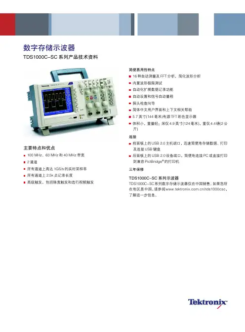
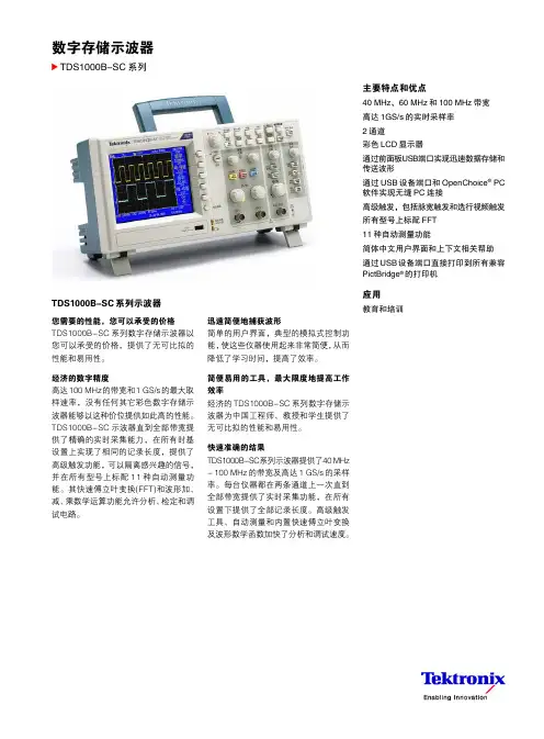
数字存储示波器TDS1000C-SC 系列产品技术资料简便易用性特点16种自动测量及FFT 分析,简化波形分析 内置波形极限测试 自动化扩展数据记录功能 自动设置和信号自动量程 探头检查向导简体中文用户界面和上下文相关帮助 5.7英寸(144毫米)有源TFT 彩色显示器体积小,重量轻:深仅4.9英寸(124毫米),重仅4.4磅(2公斤)连接前面板上的USB 2.0主机端口,迅速简便地存储数据、打印及连接USB 键盘后面板上的USB 2.0设备端口,简便地连接PC 或直接打印到兼容PictBridge ®的打印机三年保修TDS1000C-SC 系列示波器TDS1000C-SC系列数字存储示波器仅在中国销售。
如果您所在地区是中国,请参阅/tds1000csc,了解进一步信息。
主要特点和优点100 MHz、60 MHz 和40 MHz 带宽 2通道所有通道上高达1GS/s 的实时采样率 所有通道上2.5k 点记录长度高级触发,包括脉宽触发和选行视频触发产品技术资料您需要的性能,您可以承受的价格TDS1000C-SC系列数字存储示波器在紧凑的设计中提供了经济的性能。
TDS1000C-SC标配USB连接、16种自动测量、极限测试、数据记录和上下文相关帮助,帮助您在更少的时间内完成更多工作。
杰出的数字精度,实现自动测量高达100 MHz的带宽和1 GS/s的最大采样率,没有任何其它数字存储示波器能够以这种价位提供如此高的性能。
为调试设备提供关键工具高级触发如上升沿/下降沿触发、脉宽触发和视频触发帮助您迅速隔离关心的信号。
一旦捕获了信号,高级数学运算功能和自动测量功能可以加快分析速度。
您可以迅速执行FFT或波形加法、减法或乘法运算。
16种自动测量功能可以迅速可靠地计算重要的信号特点,如频率或上升时间;内置极限测试功能则可以简便地识别信号中的问题。
使用您的母语工作TDS1000C-SC系列是为您这样讲中文的用户设计的。
数字存储示波器TDS1000B-SC系列TDS1000B-SC系列示波器您需要的性能,您可以承受的价格TDS1000B-SC系列数字存储示波器以您可以承受的价格,提供了无可比拟的性能和易用性。
经济的数字精度高达100 MHz的带宽和1 GS/s的最大取样速率,没有任何其它彩色数字存储示波器能够以这种价位提供如此高的性能。
TDS1000B-SC示波器直到全部带宽提供了精确的实时采集能力,在所有时基设置上实现了相同的记录长度,提供了高级触发功能,可以隔离感兴趣的信号,并在所有型号上标配11种自动测量功能。
其快速傅立叶变换(FFT)和波形加、减、乘数学运算功能允许分析、检定和调试电路。
主要特点和优点40 MHz、60 MHz和100 MHz带宽高达1GS/s的实时采样率2通道彩色LCD显示器通过前面板USB端口实现迅速数据存储和传送波形通过USB设备端口和OpenChoice®PC软件实现无缝PC连接高级触发,包括脉宽触发和选行视频触发所有型号上标配FFT11种自动测量功能简体中文用户界面和上下文相关帮助通过USB设备端口直接打印到所有兼容PictBridge®的打印机应用教育和培训迅速简便地捕获波形简单的用户界面,典型的模拟式控制功能,使这些仪器使用起来非常简便,从而降低了学习时间,提高了效率。
简便易用的工具,最大限度地提高工作效率经济的TDS1000B-SC系列数字存储示波器为中国工程师、教授和学生提供了无可比拟的性能和易用性。
快速准确的结果TDS1000B-SC系列示波器提供了40 MHz- 100 MHz的带宽及高达1 GS/s的采样率。
每台仪器都在两条通道上一次直到全部带宽提供了实时采集功能,在所有设置下提供了全部记录长度。
高级触发工具、自动测量和内置快速傅立叶变换及波形数学函数加快了分析和调试速度。
2 数字存储示波器 /tds1000b-sc使用您的母语工作TDS1000B-SC 系列是为您这样讲中文的用户设计的。
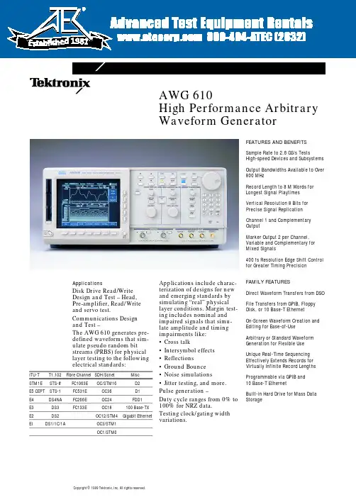
ApplicationsDisk Drive Read/Write Design and Test –Head, Pre-amplifier, Read/Write and servo test.Communications Design and Test –The AWG 610 generates pre-defined waveforms that sim-ulate pseudo random bit streams (PRBS) for physical layer testing to the following electrical standards:Applications include charac-terization of designs for new and emerging standards by simulating “real” physical layer conditions. Margin test-ing includes nominal and impaired signals that simu-late amplitude and timing impairments like:•Cross talk•Intersymbol effects •Reflections•Ground Bounce •Noise simulations•Jitter testing, and more.Pulse generation –Duty cycle ranges from 0% to 100% for NRZ data.Testing clock/gating width variations.Copyright © 1999 Tektronix, Inc. All rights reserved.AWG 610High Performance Arbitrary Waveform GeneratorFEATURES AND BENEFITSSample Rate to 2.6 GS/s TestsHigh-speed Devices and Subsystems Output Bandwidths Available to Over 800 MHzRecord Length to 8 M Words for Longest Signal Playtimes Vertical Resolution 8 Bits for Precise Signal Replication Channel 1 and Complementary OutputMarker Output 2 per Channel,Variable and Complementary for Mixed Signals400 fs Resolution Edge Shift Control for Greater Timing PrecisionFAMILY FEATURESDirect Waveform Transfers from DSO File Transfers from GPIB, Floppy Disk, or 10 Base-T Ethernet On-Screen Waveform Creation and Editing for Ease-of-Use Arbitrary or Standard Waveform Generation for Flexible Use Unique Real-Time Sequencing Effectively Extends Records for Virtually Infinite Record Lengths Programmable via GPIB and 10 Base-T EthernetBuilt-in Hard Drive for Mass Data Storage1981Real-world simulations–Corrupt ideal waveforms. Timing and amplitude signal impairments.Jitter profiles.Playback captured waveform by a DPO or DSO.Replace standard function and sweep generators in wide range of applications.High Performance AWG Family The High performance AWG family of Arbitrary Genera-tors from Tektronix can cre-ate ideal signals conforming to specific standards or “real-world” signals with speed, precision and ease. They pro-vide the highest clock speeds from 1 GS/s to 2.6 GS/s, 10 or 8 bit DAC resolution and up to 8 Mega bytes of memory depth. They combine wave-form generation and editing in one package that enables you to:•create a waveform from scratch•automatically transfer a waveform from a DPOor DSO•download signals created via computer simulation tools•modify a signal using the built-in editors These instruments can simu-late “real-world” signalimpairments such as Noise,Jitter, Fading and more.Their unique design inte-grates a graphical editing dis-play with the most powerfulhardware output capabilitiesavailable. This allows on-screen viewing of waveformediting and simplifies “what-if” test scenarios by easilyallowing the creation of com-posite signals. The familyuses a graphical user inter-face to overcome the histori-cal difficulties associatedwith developing arbitrary andcomplex waveforms. Severalintuitive and powerful tech-niques are built-in to developand edit custom waveforms.AWG 610As a premier member of theTektronix family of arbitrarygenerators, the AWG 610 isan easy-to-use, high perfor-mance, flag-ship product.The AWG 610 provides theworld’s fastest and deepestmemory with its 2.6 GS/ssample clock rate and8 Mega-points of executionmemory.The AWG 610 provides up to2 V output or 4 V into a dif-ferential input with thecomplementary output with460 MHz bandwidth at nor-mal mode (1 V output or 2 Vinto differential input withthe complementary outputwith 875 MHz bandwidth atdirect out), each with 8-Bitsvertical resolution. TheAWG 610 also provides2-channels complementary2.5 V variable marker(Tr/Tf : <150 ps @ 2V p-p)data 100 ps deskew resolu-tion at up to 2.6 GHz.System ConsiderationsThe high performance AWG610 is fully programmablevia GPIB. For throughput crit-ical applications, the AWG610 is also programmable viathe 10-Base-T Ethernet portand provides an order ofmagnitude faster data trans-fers. Its GPIB reduces the pro-gramming effort required. Asa result, it is the ideal addi-tion to provide standard andarbitrary waveform genera-tion for your system environ-ment. An optional rackmount is available for easyhardware integration intoyour test system.AWG 610 Characteristics ARBITRARY WAVEFORMSWaveform Length–512 to 8,100,032points in multiples of eight.Sequence Length–1 to 8,000 steps.Sequence Repeat Counter–1 to 65,536or infinite.CLOCK GENERATORSampling Frequency–50.000000 kHz to2.6000000 GHz.Resolution–8 digits.Internal Clock–Accuracy: ±1 ppm.Phase Noise–(data clock is 1/4th of theoutput sample rate)At 650 MHz, 10 kHz offset:–80 dBc/Hz.At 650 MHz, 100 kHz offset:–100 dBc/Hz.OPERATING MODESContinuous–Waveform is iteratively out-put. If a sequence is defined, the sequenceorder and repeat functions are applied.Triggered–Waveform is output only oncewhen an external, internal GPIB and LAN, ormanual trigger is received.Gated–Waveform begins output when gateis true and resets to beginning when false.Enhanced–Waveform is output as definedby the sequence.INTERNAL TRIGGER GENERATORInternal Trigger Rate–Range: 1.0 µs to 10.0 s.Resolution: 3 digits, 0.1 µs minimum.Accuracy: ±0.1%.MAIN OUTPUTOutput Signal–Complementary; CH1 andchannel/inverse.Digital to Analog Converter–Resolution: 8 bits.Differential Non-Linearity: ±1/2 bit.Integral Non-Linearity: ±1 bit.Output Connector–Front Panel SMA.NORMAL OUTAmplitude–Output Voltage: –2.0 V to +2.0 V into 50 Ω.Amplitude: 20 mV to 2.0 V into 50 Ω.Resolution: 1 mV.DC Accuracy: ±(1.5% of Amplitude + 2 mV)at offset = 0 V.Offset–Range:–1.000 V to +1.000 V into 50 Ω.Resolution: 1 mV.Accuracy: ±(1% of offset + 10 mV) atamplitude = 20 mV.page 2AWG 610 Characteristics ContinuedPulse Response (–1 and 1 waveform data,0 V offset, Through filter at 1V p-p):Rise time (10 to 90%): <750 ps.Fall time (10 to 90%): <750 ps.Aberrations (at 1000 MHz): At 1.0 V p-pAmplitude: ±10%.Flatness (after 20ns from rise/falledge): ±3%.Sinewave Characteristics (2.6 GS/s clock,32 waveform points, 81.25 MHz signal fre-quency, 0.5 V amplitude, 0 V offset,Through filter)–Harmonics –<–40 dBc, DC to 800 MHz.Noise –<–50 dBc, DC to 800 MHz.Phase Noise –<–85 dBc/Hz at 10 kHzoffset.FILTERType–20, 50, 100, 200 MHz Bessellow-pass.Rise time (10 to 90%)–20 MHz, 17 ns;50 MHz, 7.0 ns; 100 MHz, 3.5 ns; 200 MHz,1.75 ns.Delay from trigger–20 MHz, 50 ns +22 clock; 50 MHz, 40 ns + 22 clock;100 MHz, 35 ns + 22 clock; 200 MHz, 33 ns+ 22 clock; Through, 30 ns + 22 clock.DIRECT DA OUTAMPLITUDEOutput Voltage–-0.5 V to +0.5 V into50 Ω.Amplitude–20 mV p-p to 1.0 V p-p into 50 Ω.Resolution–1 mV.DC Accuracy–±(2% of Amplitude+ 2 mV).Offset–no function.DC Offset Accuracy–0 V ±10 mV(waveform data = 0).Pulse Response (–1 and 1 waveform data,at 0.5 V p-p)–Rise time (10 to 90%): <400 ps.Fall time (10 to 90%): <400 ps.Output Impedance–50 Ω.AUXILIARY OUTPUTSMARKERNumber–2 (complementary).Level–Hi/Lo–1.1 V to 3.0 V into 50 Ω(Max. 2.5 V p-p).-2.2 V to 6.0 V into 1 MΩ. (Max. 5 V p-p).Resolution–0.05 V.Accuracy–Within ±0.1 V +5% of setting.Rise/Fall Time (20 to 80%)–150ps(2V p-p, Hi +1V, Lo–1V) into 50 Ω.Variable Delay–Range: 0 ns to +1.5 ns.Accuracy:–30% to +10% at 1.5ms setting.Resolution: 100 ps.Marker Skew: 70 ps (typical).Connector–Front-panel SMA.10 MHz Reference Clockout–Amplitude: >1V p-p into 50 Ω. Max3V p-p open.Impedance: 50 Ω, AC coupling.Connector: Rear-panel BNC.1/4 Clock Out–Level: ECL 100 K compatible.Connector: Rear-panel BNC.Trigger In–Impedance: 1 kΩ or 50 Ω.Polarity: POS or NEG.Input Voltage Range–1 kΩ: ±10 V.50 Ω: ±5 V.Threshold–Level:–5.0 V to 5.0 V.Resolution: 0.1 V.Accuracy: ±(5% of level + 0.1 V).Pulse Width (0.2 V amplitude): 10 nsminimum.Trigger Holdoff: >576 clock + 450 ns.Delay to Marker: 28ns + 22 clock.Delay to Analog Out: (typical)(filter through)30 ns + 22 clock (trigger)30 ns + 880 clock (gate)Connector: Rear-panel BNC.Event Trig Input–Number of Events: 4 bits.Input Signals: 4 event bits, strobe.Threshold: TTL level.Pulse Width: 128 clocks minimum.Maximum Input: 0 V to +5 V (DC+ peak AC).Delay to Analog Out: 850 clock + 20ns(ASYNC mode).Impedance 2.2 kΩ, pull-up to +5 V.Connector: Rear-panel 9-Pin D-sub.Reference 10 MHz Clock IN–Input Voltage Range: 0.2 V to 3.0 V p-p,±10 V maximum.Impedance: 50 Ω, AC coupled.Frequency Range: 10 MHz ±0.1 MHz.Connector: Rear-panel BNC.AWG 610 General Characteristics DISPLAYArea–13.2 cm (5.2 in.) horizontal by9.9 cm (3.9 in.) vertical.Resolution–640 horizontal by 480 verticalpixels.DATA STORAGEInternal Hard disk Drive–2.1 Gbytes.(standard)Floppy Disk Drive–3.5 inches,1.44 MbytesOption 10–Flash Disk replaces HDD,78Mbytes.ENVIRONMENTAL, EMC, SAFETYTemperature–Operating: 10°C to +40°C.Non-operating: –20°C to +60°C.Humidity–Operating: 20 to 80%, non-condensing.Non-operating: 5 to 90%, non-condensing.Altitude–Operating: Up to 4,500 m. (15,000 ft). Maxi-mum operating temperature decreases 1°Cper 300 m above 1.5 km.Non-operating: Up to 15,000 m (50,000 ft.).Vibration (test limits)–Operating: 0.27 g RMS from 5 to 500 Hz,10 minutes.Non-operating: 2.28 g RMS from 5 to500 Hz, 10 minutes.Shock (test limits)–Non-operating: 294 m/s2(30 g), half-sine,11 ms duration.EMC Compliance–EN50081-1., EN50082-1.AS/NZS 20641/2.Safety Compliance–UL 3111-1., CSA C22.2 No. 1010.1.EN61010-1 with second amendment.page 3AWG 610GeneralCharacteristics ContinuedPOWER Source Power –Line Voltage Range: 100 to 240 VAC.Line Frequency: 48 to 63 Hz.Power Consumption –600 W at 8 A .PHYSICAL CHARACTERISTICSWidth 42216.6Weight kg lb.WARRANTYOne year parts and labor.OTHERProgrammable Interface –GPIB: 24-Pin IEEE488.1 connector.Ethernet: 10Base-T, RJ-45 connector.Keyboard Connector –6-Pin mini-DIN connector.4/99 HB/XBS76W-12991-0Copyright © 1999, Tektronix, Inc. All rights reserved. Tektronix products are covered by U.S. and foreign patents, issued and pending. Information in this publication supersedes that in all previously published material. Specification and price change privileges reserved. TEKTRONIX and TEK are registered trademarks of Tektronix, Inc. All other trade names referenced are the service marks, trademarks or registered trademarks of their respective companies.。

222A 222PS 224Handheld Digitizing Oscilloscopeso MC9 csCapture yourmeasurements inout of the wayplaces with thesebattery operated.compact,industrial servicedigitizing scopes.222A/222PS/224• Isolated ChannelArchitecture• Floatable to±850 V/channel(222PS, 224)±400 V/channel(222A)• 10 MHz 222A,10 MHz222PS,60 MHz 224• 100 ns GlitchCapture• 6 kV Peak SurgeRating(222PS, 224)• Exclusive MotorTrigger (222PS)•Video Line Trigger(224)•Auto Trigger• Save ReferenceMemory• Dual 10 MS/sDigitizers• Programmablevia RS-232-C• Auto Setup• Save Setup• Detachable 1X/10XProbes• RuggedConstruction• Battery Operated• 4.4 lbs222A/222PS/224The 220 Series of scopes provides unsurpassed power in the world of handheld oscilloscopes. The 60 MHz 224 and the 10 MHz222A and 222PS sample at 10 MS/s for eachchannel, have an RS-232-C interface, andare fully programmable. Internal batterieseliminate the need for external power. Thesehandheld scopes can also charge and operatefrom 12-28 V D C or 16-20 VAC.UNMATCHED SAFETYTo ensure ultimate operator safety, the channels are fully isolated from each other and thecasing is double insulated. Because they arefloatable to ±850 V per channel, the 224 andthe 222PS can make measurements safely onindustrial power systems. They are the firstscopes to be UL listed for line voltage measurements to 600 V AC, and are specified towithstand peak surges as high as 6 kV. The222A can safely measure +400 V per channelor800Vp-p.UNMATCHED VERSATILITYThe 224, because of its size, bandwidth, andportability, is a perfect tool for high-speedelectronics that can’t be easily returned to arepair shop, such as ATMs or avionics. The224’s exclusive TV trigger makes it just thething for servicing medical imaging systemsor closed-circuit surveillance equipment.UNMATCHED FEATURESAuto Setup and Save/Recall limit the need formanipulation of the front panel. Pushing theAuto Setup button selects all the input parameters for you. Save/Recall boosts productivity in repetitive testing at different locationsby saving up to four front-panel setups.After you’ve acquired a waveform using AutoSetup, you may save it in one of four 512 byterecords. Then, recall a known good signal forcomparison and make the necessary adjustments to bring the equipment on line.To make a permanent record, simply connectthe scope to your PC via the RS-232-C interface and transfer waveforms and setupsusing the optional CAT200 Software. Sendthem back to the scope when that same job isdue again. With CAT200 Software, you cancontrol the entire front panel from a remotelocation using the RS-232-C port, a modem,and a phone line.The WP200 Intelligent Printer Interface allowsyou to make a hardcopy of a displayed waveform on an Epson-compatible printer-without using a P C and dedicated software.UNMATCHED RUGGEDNESSThe 220 Series is packaged in impact-resistant plastic, capable of withstanding 50 g’s ofshock. They can operate accurately to temperatures as low as -10°C. The batteriesallow a minimum of three hours of operation.Each scope comes complete with a ballisticnylon carrying case with a neck strap forhands-free operation.Product(s) availablethrough an AuthorizedTektronix Distributor.S e e pages 590-595.IS O 9061T e k tro n ix M e a s u re m e n tp ro d u c ts a re m a n u fa c tu re d inIS O re g is te re d(B e little s.A P P L I C A T I O N S• Power M easurem ents• M oto r Drive Test• E le ctro n ic Device Debug• TV and Video Signal Troubleshooting• S a fe H lg b-v o lta g a M e a s u re m e n ts• R e m o t e S ig n a l M o n ito rin g a n d S e r v ic e(w ith C A T200s o ftw a re)• U s e f u l In L o w T e m p e r a t u r ee n v i r o n m e n t s114-Handheld Digitizing Oscilloscopes 222A 222PS 224KEY S P E C IF IC A T ONS CO222A222P S224LU Bandwidth10 MHz10 MHz60 MhDigitizers/Channels 2 %fc= -r:h rfJ2O Rise Time35 n s35 ns i i a i i s B l l l M B I I M l i i l l'C OSample Rate (each channel) Vertical Resolution lOMS/s8-BitlOMS/s8-Bitioiife/s '■w it.eVertical Sensitivity 5 m V to 50 V/tfiv50 mV to 500 V/div5OffiVto5G0WdivSweep Speed 5 ns to 20 s/d B v 5 ns to 20 s/div5 ns to 26 s/div o Time Base S ingle Single C U mm I u i t/iAcquisition Modes N orm al A vetaging P e a k D e te c t,Accum ulated P e a k Normal, Averaging, Peak Detect,Accumulated PeakN o rm a l A v e ra g in g P e a k D e te c tA cru tm ila te d P e a kee sPeak Detect/Glitch Capture Record Length100 ns512 bytea100 ns512 bytes100 ft*512 bytesIndependently Floatable Isolated Channels±400 V(D C or pkAC)±850 V(DC or pk AC)or 600 VAC±859 V(D C or$kAC)or 600 VACH*Motor Trigger-Yes C5 Video Field and Line Trigger-:-Ytii!"o I/O Interface R S-232*C - »’ ■:RS-232-C RS-2&CMinimum Battery Life 3 hours 3 hours o Battery Charge Time 3 hou|i " 3 hours3Ujug.................................Warranty3 years 3 yearsSafety Certification UL.CSA UL, CSA...............QR D E R I N G I N F O R M A T I O N222A10 MHz Handheld DSOIncludes: Operator’s Manual, Quick Reference Guide, RS-232-C Guide, AC Adapter, Two P400IX Replaceable Probes, Pouch, Feet, Probe Accessory Kit222P S10 MHz Handheld DSOIncludes: Operator’s Manual, Quick Reference Guide, RS-232-C Guide, AC Adapter, Two P850 10X Replaceable Probes, Pouch, Feet, Probe Accessory Kit, Industrial Lead Set22460 MHz Handheld DSOIncludes: Operator’s Manual, Quick Reference Guide, RS-232-C Guide, AC Adapter, Two P850 Replaceable Probes, Pouch, Feet, Probe Accessory KitO p t. 02 - Delete AC adapterO pt. 03 - Substitute P850 Probes for P400 (222A only)IN T E R N A T IO N A L P O W E R P L U G O P T IO N SO pt. A1 - Univ Euro 220 V, 50 HzO p t. A2 - United Kingdom 220 V, 50 HzS E R V IC E A S S U R A N C E O P T IO N SThese products covered by the following service assurance options: R E P4200 - Provides One Year of Post-Warranty Repair Protection CAU200 - Provides One Year of Calibration Services A V A IL A B L E A C C E S S O R IE SVirtual Instrum ent Software - Order CAT200E xternal Battery C h arger - Order BAT200P o u c h for Battery/A C Adapter - Order 016-0993-00Viewing H o o d - Order 016-1021-00E X T Trig to B N C Adapter - Order 103-0090-00U S 120 V Pow er A dapter - Order 120-1807-00Spare Battery - Order 146-0075-00R S-232 Cable - Order 174-1453-00Cigarette Lighter Adapter - Order 174-1734-00Intelligent Printer Interface - Order WP200X10 B N C Adapter - Order 206-0445-00Industrial Le a d Set - Order 012-1392-00B NC P ro be H e a d - Order 206-0451-00O P E R A T IO N V ID E O T A P EN T S C-O rder 068-0344-04PA L-O rder 068-0344-06S E C A M - Order 068-0344-07P R O S E SVoltage -IX. Order P40010X. Order P850C urrent -AC Current, 2000 A pk. Order A620External Trigger - Order P6122Product(s) availablethrough an AuthorizedTektronix Distributor.See pages 590-595.1SSTOT e k tro n ix M e a s u re m e n tp ro d u c ts a r e m a n u fa c tu re d I nI S O re g is te re d fa c ilitie s.115。
1、什么是任意波形发生器,与函数发生器的区别,如何产生任意波形信号,“任意”如何理解2、任意波形发生器的基本原理答:以DDS技术为基础,通过改变DDS中的查找表的数据,来实现任意波形。
根据所采用DDS的结构不同,采用DDFS结构的叫做函数/任意波形发生器,以Agilent的33250和Tektronix的AFG3000系列为典型代表,采用DDWS 结构的叫做任意波形发生器,以Tektronix的AWG5000和AWG7000系列为代表3、任意波形发生器的形式答:大体上分为两种——台式仪器和模块式仪器,台式仪器如Agilent的33250,33120,tektronix的AFG和AWG系列等,模块化仪器包括VXI、PXI、cPCI、LXI(部分LXI模块也提供键盘、显示,可划归为台式仪器)、USB接口模块仪器等4、任意波形发生器的结构,每部分的作用,完成的功能,以及相应的对外接口信号?答:主要包括CPU模块、任意波形合成模块、模拟通道、电源四大组成部分1)CPU模块a)主控制器(包括单片机、ARM嵌入式处理器、PC机等,有板载CPU和非板载CPU之分,如台式仪器、VXI模块是板载CPU,而PXI模块是非板载CPU)b)键盘模块(台式仪器所特有,包括功能键、数字键以及飞梭)c)程控接口模块(一般为台式仪器特有,包括USB,LAN,GPIB,RS232等)d)显示模块(一般为台式仪器特有,有些模块化仪器也提供VGA接口,支持外接显示器的功能)2)任意波形合成模块a)时钟发生模块●在参考时钟(一般为10MHz,其准确度决定了采样时钟及输出频率的准确度)的作用下,产生波形DAC模块所需的采样时钟。
如果为DDFS架构,采样时钟为固定频率,如果为DDWS架构,采样时钟为可变频率。
●提供外部参考时钟和内部参考时钟的切换功能(有两种方法,一种是参考时钟内外源自动切换,当有外部参考时钟接入时,自动切换到外部参考时钟;一种是手动切换,并且当外部参考时钟超过一定范围时,自动切换到内部参考时钟)●提供内/外部采样时钟的切换功能(不是所有的仪器都有,一般在高档仪器上才有)●提供仪器内部所需的一些时钟信号,如调制模块中ADC所需的采样时钟、触发模块中所需的触发信号产生器的计数时钟等思考:1、为什么要提供外部采样时钟,作用是什么?2、如何用参考时钟产生采样时钟?方法有哪些?b)地址产生模块——产生波形存储器模块所需的寻址信号●累加器模块——对送入的频率控制字进行累加操作,产生相应的寻址信号;累加器模块应提供清零信号输入,通过控制清零信号,可产生Burst调制波形输出●相位加法器模块●频率控制字生成模块——产生累加器所需的频率控制字,可实现调频、扫频、FSK调制●相位控制字生成模块——产生相位加法器所需的相位控制字,可实现调相、PSK调制●地址位数选择模块——选择输出地址的位数,一般来说,当任意波形发生器工作在函数模式时,地址位数选择为16位,有利于在保证波形质量的前提下提供切换速度;当工作在任意波形模式时,将提供最大的地址输出能力(视存储容量而定)c)存储器模块●存储器(目前一般采用ZBT SRAM,也有采用DDR SDRAM,QDRSRAM或异步SRAM的),根据所要实现的采样率不同,也分为单片存储器和多存储器并行两种模式,具体参见多存储器并行任意波形合成技术●存储器管理模块——负责管理存储器地址线、数据线、读、写、片选等,注意任意波形的工作过程,1、由CPU将所需的波形数据写入波形存储器中,此时,存储器的地址、数据、写、片选都由CPU提供,读信号无效;2、地址产生模块提供地址信号连续读取存储器的波形数据,此时,存储器的地址由地址产生模块提供,读、片选均应一直使能,写信号无效,读取的数据送数据合成模块d)数据合成模块●对存储器传入的波形数据进行处理后传送给波形DAC模块●处理包括调幅、数据插值(并串转换)等e)波形DAC模块f)调制模块●产生内部调制时所需的调制波形数据(调频、调幅、调相和SWEEP需要)●对外部调制源送入的调制信号通过ADC进行采样,采样后产生相应的调制波形数据●进行调制源选择●产生Burst调制所需的清零控制信号g)触发模块●产生内部触发信号●对触发信号进行触发极性选择●进行触发源选择h)同步Marker模块●产生同步Marker数字信号●对产生的Marker数字信号进行幅度控制等i)方波产生模块●在Stratix3及其以上的器件中实现,通过数字的方法产生占空比精密可调的方波信号、脉宽精密可调的脉冲信号以及PWM调制波形信号3)模拟通道模块(根据模拟输出的指标不同而略有区别)a)滤波器模块b)脉冲沿调整模块c)幅度控制模块d)衰减模块e)放大模块f)加偏模块一、任意波形发生器的接口及指标1、主输出:波形信号的输出主要指标包括:工作模式:连续、触发、门控、序列输出特性:输出样式:单端或差分输出阻抗:50欧姆或75欧姆输出幅度范围、分辨力、准确度输出偏移范围、分辨力、准确度输出波形种类、频率范围、频率准确度输出正弦信号谐波失真、非谐波失真、SFDR、相位噪声方波上升、下降时间、占空比、过冲调制波形种类以及调制的参数(具体在调制部分再介绍)DAC垂直分辨位数存储深度2、时钟电路部分(通道共用)(1)内部参考输出:输出仪器内部晶振产生的参考时钟信号,该信号可用于同步多台任意波形发生器,或同步任意波形发生器和其它仪器。
使用任意波形发生器创建无线信号入门手册使用任意波形发生器创建无线信号入门手册2 /signal_generators使用任意波形发生器创建无线信号入门手册目 录摘要⋯⋯⋯⋯⋯⋯⋯⋯⋯⋯⋯⋯⋯⋯⋯⋯⋯⋯⋯⋯⋯⋯⋯⋯⋯⋯⋯⋯⋯⋯⋯⋯⋯⋯⋯⋯⋯⋯⋯⋯⋯⋯⋯⋯⋯⋯4简介⋯⋯⋯⋯⋯⋯⋯⋯⋯⋯⋯⋯⋯⋯⋯⋯⋯⋯⋯⋯⋯⋯⋯⋯⋯⋯⋯⋯⋯⋯⋯⋯⋯⋯⋯⋯⋯⋯⋯⋯⋯⋯⋯⋯⋯⋯4无线应用与数字调制⋯⋯⋯⋯⋯⋯⋯⋯⋯⋯⋯⋯⋯⋯⋯⋯⋯⋯⋯⋯⋯⋯⋯⋯⋯⋯⋯⋯⋯⋯⋯⋯⋯⋯⋯⋯⋯⋯5-12无线发射面临的挑战⋯⋯⋯⋯⋯⋯⋯⋯⋯⋯⋯⋯⋯⋯⋯⋯⋯⋯⋯⋯⋯⋯⋯⋯⋯⋯⋯⋯⋯⋯⋯⋯⋯⋯⋯⋯⋯5为什么要数字调制?⋯⋯⋯⋯⋯⋯⋯⋯⋯⋯⋯⋯⋯⋯⋯⋯⋯⋯⋯⋯⋯⋯⋯⋯⋯⋯⋯⋯⋯⋯⋯⋯⋯⋯⋯⋯⋯6什么是数字调制?⋯⋯⋯⋯⋯⋯⋯⋯⋯⋯⋯⋯⋯⋯⋯⋯⋯⋯⋯⋯⋯⋯⋯⋯⋯⋯⋯⋯⋯⋯⋯⋯⋯⋯⋯⋯⋯⋯7数字调制应用⋯⋯⋯⋯⋯⋯⋯⋯⋯⋯⋯⋯⋯⋯⋯⋯⋯⋯⋯⋯⋯⋯⋯⋯⋯⋯⋯⋯⋯⋯⋯⋯⋯⋯⋯⋯⋯⋯⋯⋯12数字无线测试⋯⋯⋯⋯⋯⋯⋯⋯⋯⋯⋯⋯⋯⋯⋯⋯⋯⋯⋯⋯⋯⋯⋯⋯⋯⋯⋯⋯⋯⋯⋯⋯⋯⋯⋯⋯⋯⋯⋯⋯⋯12-19发射机-I-Q调制器测试⋯⋯⋯⋯⋯⋯⋯⋯⋯⋯⋯⋯⋯⋯⋯⋯⋯⋯⋯⋯⋯⋯⋯⋯⋯⋯⋯⋯⋯⋯⋯⋯⋯⋯⋯13 IF滤波器效率和损伤测试⋯⋯⋯⋯⋯⋯⋯⋯⋯⋯⋯⋯⋯⋯⋯⋯⋯⋯⋯⋯⋯⋯⋯⋯⋯⋯⋯⋯⋯⋯⋯⋯⋯⋯⋯14发射机-RF功率放大器线性度⋯⋯⋯⋯⋯⋯⋯⋯⋯⋯⋯⋯⋯⋯⋯⋯⋯⋯⋯⋯⋯⋯⋯⋯⋯⋯⋯⋯⋯⋯⋯⋯⋯15接收机-IF解调器测试⋯⋯⋯⋯⋯⋯⋯⋯⋯⋯⋯⋯⋯⋯⋯⋯⋯⋯⋯⋯⋯⋯⋯⋯⋯⋯⋯⋯⋯⋯⋯⋯⋯⋯⋯⋯16接收机-RF功能测试⋯⋯⋯⋯⋯⋯⋯⋯⋯⋯⋯⋯⋯⋯⋯⋯⋯⋯⋯⋯⋯⋯⋯⋯⋯⋯⋯⋯⋯⋯⋯⋯⋯⋯⋯⋯17接收机-平衡器特性评估⋯⋯⋯⋯⋯⋯⋯⋯⋯⋯⋯⋯⋯⋯⋯⋯⋯⋯⋯⋯⋯⋯⋯⋯⋯⋯⋯⋯⋯⋯⋯⋯⋯⋯⋯18接收机-干扰灵敏度⋯⋯⋯⋯⋯⋯⋯⋯⋯⋯⋯⋯⋯⋯⋯⋯⋯⋯⋯⋯⋯⋯⋯⋯⋯⋯⋯⋯⋯⋯⋯⋯⋯⋯⋯⋯⋯18 RF频谱环境仿真⋯⋯⋯⋯⋯⋯⋯⋯⋯⋯⋯⋯⋯⋯⋯⋯⋯⋯⋯⋯⋯⋯⋯⋯⋯⋯⋯⋯⋯⋯⋯⋯⋯⋯⋯⋯⋯⋯⋯19使用任意波形发生器(AWG)生成调制信号⋯⋯⋯⋯⋯⋯⋯⋯⋯⋯⋯⋯⋯⋯⋯⋯⋯⋯⋯⋯⋯⋯⋯⋯⋯⋯⋯⋯19-25生成基带I-Q信号⋯⋯⋯⋯⋯⋯⋯⋯⋯⋯⋯⋯⋯⋯⋯⋯⋯⋯⋯⋯⋯⋯⋯⋯⋯⋯⋯⋯⋯⋯⋯⋯⋯⋯⋯⋯⋯⋯19 IF生成⋯⋯⋯⋯⋯⋯⋯⋯⋯⋯⋯⋯⋯⋯⋯⋯⋯⋯⋯⋯⋯⋯⋯⋯⋯⋯⋯⋯⋯⋯⋯⋯⋯⋯⋯⋯⋯⋯⋯⋯⋯⋯⋯20 RF生成⋯⋯⋯⋯⋯⋯⋯⋯⋯⋯⋯⋯⋯⋯⋯⋯⋯⋯⋯⋯⋯⋯⋯⋯⋯⋯⋯⋯⋯⋯⋯⋯⋯⋯⋯⋯⋯⋯⋯⋯⋯⋯⋯21编译复合信号⋯⋯⋯⋯⋯⋯⋯⋯⋯⋯⋯⋯⋯⋯⋯⋯⋯⋯⋯⋯⋯⋯⋯⋯⋯⋯⋯⋯⋯⋯⋯⋯⋯⋯⋯⋯⋯⋯⋯⋯23回绕式考虑⋯⋯⋯⋯⋯⋯⋯⋯⋯⋯⋯⋯⋯⋯⋯⋯⋯⋯⋯⋯⋯⋯⋯⋯⋯⋯⋯⋯⋯⋯⋯⋯⋯⋯⋯⋯⋯⋯⋯⋯⋯24展望⋯⋯⋯⋯⋯⋯⋯⋯⋯⋯⋯⋯⋯⋯⋯⋯⋯⋯⋯⋯⋯⋯⋯⋯⋯⋯⋯⋯⋯⋯⋯⋯⋯⋯⋯⋯⋯⋯⋯⋯⋯⋯⋯⋯⋯⋯26/signal_generators 3使用任意波形发生器创建无线信号入门手册图1. Tektronix AWG 系列简化方框图揭示了一个可变时钟控制任意波形,采样速率达20 GS/s摘要任意波形发生器(AWG)已经在商业上应用数年并在性能上不断得到改进。
先进的任意波形发生器如最新的Tektronix AWG系列可以支持今天最复杂的无线测试信号。
现代AWG可以产生基带、IF和RF频带激励信号以高效率地测试无线器件和系统性能。
20 GS/s,10位深度分辨率的AWG7000可以适用在极端的应用环境当中,如超宽带(UWB)无线电设计。
类似的,14位深度分辨率AWG5000可以适合在高动态范围的窄带应用。
当合成复合数字无线调制时,任意波形发生器的独特价值得以快速显现。
在此入门介绍中,我们探讨推进数字无线革新的技术,一些通用的AWG无线测试应用以及如何从任意波形发生器得到更好特性的重要思路。
简介近年来无线设备行业成长迅速并产生了许多新型无线设备。
行业发展迅猛的重要原因在于RF半导体的发展和数字调制技术的广泛应用。
如今的数字无线信号对合成测试信号提出一系列新的挑战。
由于行业重点向数字无线技术转移,使得调制波形复杂度极速增加。
幸运的是AWG性能稳定上升能够灵活有效地产生相当复杂的测试激励信号。
AWG的原理很简单,一个可变频率时钟步进跟随一个任意波形的预存储数字表达,然后被转换为模拟信号。
尽管概念简单,但在每次测试应用中为获得AWG的最佳性能,各种重要思路是必要的。
为了理解如何得到AWG的最佳性能,我们首先回溯RF传输信道,说明为什么复合数字调制受人欢迎。
4 /signal_generators使用任意波形发生器创建无线信号入门手册此入门简介参考了一些普通无线测试案例,随后是AWG 在基带、IF和RF应用中的重要思路。
最后是RF测试中AWG应用的前景展望总结。
无线应用程序和数字调制由于现在多数复杂射频调制波形具有预期特性,因此被选用来抗击无线传输通道。
介于传输器和接收器之间,该信号必须通过的的传输通道媒介由分配给信号的射频通道频带宽度界定。
无线传输的挑战通过无线通道的传输和接收电磁辐射可能面临着挑战。
传输通道通常会大大削减被传输信号,同时其噪音和传播特性会彻底扭曲传输波形。
从无线电到雷达的无线应用程序跨越了广泛的通道类型。
无线信号传播依赖于传输信号的频率和带宽,以及附近的反射和吸收物体。
大气和电离层等客观条件也会在传输信号达到接收终端时使其发生较大改变。
为了达到使用性的目的,调制传输信号在通过接受器时,受到严重路径减损后必须是可恢复的。
比如1瓦(+30 dBm)传输信号可能会在其达到接收器的同时被削减到其最初振幅 (-90 dBm) 的一万亿分之一。
如果存在多路经,那么通过传输带宽的衰减就不可能一致。
通道的衰减和迟滞还可能随着接收器的物理运动而有所波动。
最近几年,宽带信号因其能够抗击波动通道获得了普及。
超宽带调制技术能够通过填充有多路经的,分散的传输通道传递高速数据。
然而,许多测试信号发生器完全不能生成超宽带信号所需要的宽的带宽和成就一个重要的发展及测试障碍。
在深入探讨超宽带挑战和生成技术之前,让我们先看一看数字调制是什么以及为什么它们如此普遍。
图2 不使用任意波形发生器时,图中所示的64 QAM 信号包含波形的复合调制将难以合成图 3. 无线信号经受各种会严重改变传输信号的通道作用。
为提高接收效果,复杂数字调制会起到举足轻重的作用。
/signal_generators 5使用任意波形发生器创建无线信号入门手册为什么会有数字调制?调幅(AM),调频 (FM) 和调相 (PM) 在数字调制日趋普遍之前被广泛采用模拟调变。
模拟调变的首要问题是传输信号是不予以编码的。
模拟信号完全被调制并依附于一个高频射频载体上,其将通过传输通道进行传播。
例如,一个扩音器的模拟电压是被直接调制到一个广播射频载体上的典型调频。
由于没有编码,在接收器解调信号后,达到的模拟信号强度与噪音强度的比率(S/N or SNR) 取决于射频载体的信号强度的作用。
完成具有广泛动态范围的静态自由传输—因此被解调噪音程度非常小,被比成是所需信号的振幅—需要非常高的射频S/N比率。
由于传输通道的背景热力噪音动力光谱密度通常固定在-174 dBm/Hz,因此唯一提高模拟调制接收质量的方法就是传输较高动力水平,使用较大和较多的方向天线,或者在较宽的带宽上进行调制。
这些模拟调制局限会限制能够通过传输通道实现的动态范围性能。
然而,唯一能够传送低射频S/N比率的高动态范围的只有数字调制。
数字调制通过把即将发送的信号编码成另一个要求低射频S/N比率的形式,以便成功接收。
比如,扩音器的一图4.模拟信号需要高的射频S/N比率以便在解调后仍是高的S/N比率。
数字调制在给低射频S/N比率解调加入一点精密度后能够达到非常高的S/N比率。
个电压能够被数字化并被编码成一个8位字。
然后每一位被使用简单的二进位判断法来准确确定正确字节,并以较低射频S/N比率传送出去。
当所有字节在接收器中被重新合成一个8位字时,一个48 dB动态范围就产生了,即使射频通道可能仅有25 dB的S/N比率。
接受器末端的信号保真度多数情况下是固定的,大于数字调制可接受的字节错误率所需的最小S/N比率。
这些特性使得数字调制在遭受传输通道的严重损害后,不仅可以消除静态噪音,还提供了优异的通信可靠性。
6 /signal_generators/signal_generators 7使用任意波形发生器创建无线信号入门手册图5. 在1个RSA3408A 实时光谱分析机(RTSA)上抓取的无线电话的传输显示了两种频率、两种程度的FSK 信号及恢复特征。
数字调制通常还具有许多优于模拟调制的其他优点。
其中一个优点就是其使得数字模拟的普遍使用直接来自于使用的数字信号处理器(DSP)以生成调制。
现在大部分数字调制都是由某种数字电路形式的DSP技术产生的,例如现场可编程门阵列(FPGA),或者专门的DSP 微处理器。
相比较许多模拟电路,数字电路更加稳定,不会随着温度变化而变化。
数字电路的稳定,精确和可靠减少了温度模拟设计和手动电路调整,节省了大量的生产劳力。
这不仅节约了成本,而且还推动了可行性技术的发展。
同模拟调制相比,数字调制通常被使用者称赞是大大减小了波谱带宽,其实不尽然。
许多当下流行的数字调制大体上并非比流行模拟调制更具带宽有效性。
然而,由于数字数据在被传送到调制器之前能够被压缩,因此固定的信息带宽缩减通常是可以的。
所以,数字信号压缩技术和一个数字调制器的混用通常达到所需射频带宽数量的3:1的缩减,以便传送多种类型的无线数据。
为更好理解数字调制的带宽特性和了解AWG对于生成复杂波形的举足轻重的作用。
让我们现在思考一下用来传送二进位‘1’和‘0’⋯的波形。
什么是数字调制?数字调制同模拟调制,各种射频振幅,频率或相位类似,但是通过数字调制,被调制参数可呈现出一特定波形状态或特征。
相反,模拟调制由于振幅、频率或相位而发生不断变化。
简单的数字调制例如幅移键控(OOK),双移频键控(FSK),或二相相移键控(BPSK)仅使用两种状态就表示出了二进位编码数据。
通过这些简单的双状态调制,每一编码状态或特征就代表了二进位1或者0。
OOK, FSK 和BPSK 提供良好的动力效率,并能够被以S/N 比率可靠接收。
然而,这些调制都具有很差的带宽效率,这就意味着对于一个给定的数据比率(bits/s),射频传输通道带宽是调制后所必需的。
相比之下,动力效率调制在有限的通道带宽内,达不到非常高的数据比率。
容易看到的一个现象就是把带宽效率平面上这些简单调制的动力效率当成给定比特误差率(BER)的其他调制。
2FSK 和 BPSK的低Eb/No 或 S/N比率使得它们在接收动力受到限制的地方能引起注意。