M74HCT245中文资料
- 格式:pdf
- 大小:268.54 KB
- 文档页数:11
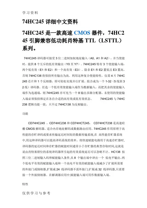
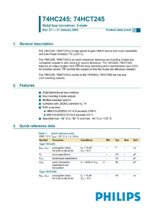
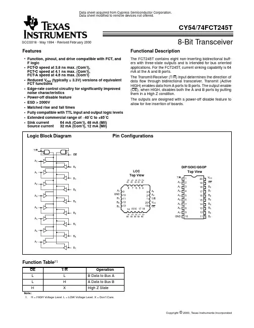
M54/74HCT245/640/643M54/74HCT245/640/643October 1993HCT640INVERTING,HCT643INVERTING/NON INVERTINGOCTAL BUS TRANSCEIVER (3-STATE):HCT245NON INVERTINGB1R(Plastic Package)ORDER CODES :M54HCTXXXF1R M74HCTXXXM1R M74HCTXXXB1R M74HCTXXXC1RF1R(Ceramic Package)M1R(Micro Package)C1R (Chip Carrier)PIN CONNECTION (top view).HIGH SPEEDt PD =10ns (TYP.)at V CC =5V .LOW POWER DISSIPATIONI CC =4µA (MAX.)at T A =25oC.COMPATIBLE WITH TTL OUTPUTS V IH =2V (MIN.)V IL =0.8V (MAX.).OUTPUT DRIVE CAPABILITY 15LSTTL LOADS.SYMMETRICAL OUTPUT IMPEDANCE |I OH |=I OL =6mA (MIN).BALANCED PROPAGATION DELAYS t PLH =t PHL.PIN AND FUNCTION COMPATIBLE WITH 54/74LS245/640/643DESCRIPTIONThe M54/74HCT245,HCT640and HCT643utilise silicon gate C 2MOS technology to achive operating speeds eqivalent to LSTTL devices.Along with the low power dissipation and high noise immunity of standad CMOS integrated circuit,it possesses the capability to drive 15LSTTL loads.These IC’s are intended for two-way asynchronous communication between data buses,and the direction of data trasmission is determined by DIR input.The enable input (G)can be used to disable the device so that the buses are effectively isolated.All input are equipped with protection circuits against static discharge and transient discharge.These integrated circuits have input and output characteristics that are fully compatible with 54/74LSTTL logic families.M54/74HCT devices are designed to directly interface HSC 2MOS systems with TTL and NMOS components.They are also plug in replacements for LSTTL devices giving a reduction of power consumption.IT IS PROHIBITED TO APPLY A SIGNAL TO A BUS TERMINAL WHEN IT IS IN OUTPUT MODE AND WHEN A BUS THERMINAL IS FLOATING (HIGH IMPEDANCE STATE),IT IS REQUESTED TO FIX THE INPUT LEVEL BY MEANS OF EXTERNAL PULL DOWN OR PULL UP RESISTOR.HCT245HCT640HCT6431/11INPUT AND OUTPUT EQUIVALENT CIRCUITPIN DESCRIPTIONPIN No SYMBOL NAME AND FUNCTION 1DIR Directional Control 2,3,4,5,6,7,8,9A1to A8Data Inputs/Outputs 18,17,16,15,14,13,12,11B1to B8Data Inputs/Outputs19G Output Enabel Input (Active LOW)10GND Ground (0V)20V CCPositive Supply VoltageIEC LOGIC SYMBOLSTRUTH TABLEINPUT FUNCTIONOUTPUT G DIR A BUS B BUS HCT245HCT640HCT643L L OUTPUT INPUT A =B A =B A =B L H INPUT OUTPUTB =A B =A B =A HXZZZZZX:”H”or ”L”Z:High impeda nceHCT245HCT640HCT643M54/M74HCT245/640/6432/11M54/M74HCT245/640/643 LOGIC DIAGRAM(HCT640)NOTE:IN CASE OF HCT245OR HCT643,INPUT INVERTERS MARKED*AT A BUS AND B BUS ARE ELIMINATED RESPECTIVELYABSOLUTE MAXIMUM RATINGSSymbol Parameter Value Unit V CC Supply Voltage-0.5to+7V V I DC Input Voltage-0.5to V CC+0.5V V O DC Output Voltage-0.5to V CC+0.5VI IK DC Input Diode Current±20mAI OK DC Output Diode Current±20mAI O DC Output Source Sink Current Per Output Pin±35mAI CC or I GND DC V CC or Ground Current±70mAP D Power Dissipation500(*)mW T stg Storage Temperature-65to+150o C T L Lead Temperature(10sec)300o C Absolute Maximum Ratings are those values beyond whichdamage to the device may occu r.Functiona l ope ration und er these cond ition isnotimplied. (*)500mW:≅65o C derate to300mW by10mW/o C:65o C to85o C3/11RECOMMENDED OPERATING CONDITIONSSymbol Parameter Value Unit V CC Supply Voltage 4.5to5.5V V I Input Voltage0to V CC V V O Output Voltage0to V CC VT op Operating Temperature:M54HC SeriesM74HC Series -55to+125-40to+85o Co Ct r,t f Input Rise and Fall Time(V CC=4.5to5.5V)0to500ns DC SPECIFICATIONSSymbol ParameterTest Conditions ValueUnit V CC(V)T A=25o C54HC and74HC-40to85o C74HC-55to125o C54HCMin.Typ.Max.Min.Max.Min.Max.V IH High Level InputVoltage 4.5to5.52.0 2.0 2.0VV IL Low Level InputVoltage 4.5to5.50.80.80.8VV OH High LevelOutput Voltage4.5V I=V IHorV ILI O=-20µA 4.4 4.5 4.4 4.4VI O=-6.0mA 4.18 4.31 4.13 4.10V OL Low Level OutputVoltage4.5V I=V IHorV ILI O=20µA0.00.10.10.1VI O=6.0mA0.170.260.330.4I I Input LeakageCurrent 5.5V I=V CC or GND±0.1±1±1µAI OZ3State OutputOff State Current5.5V I=V CC or GND±0.5±5.0±10µAI CC Quiescent SupplyCurrent5.5V I=V CC or GND44080µA∆I CC Additional worstcase supplycurrent 5.5Per Input pinV I=0.5V orV I=2.4VOther Inputs atV CC or GNDI O=02.0 2.93.0mAM54/M74HCT245/640/643 4/11AC ELECTRICAL CHARACTERISTICS(C L=50pF,Input t r=t f=6ns)Symbol ParameterTest Conditions ValueUnit V CC(V)C L(pF)T A=25o C54HC and74HC-40to85o C74HC-55to125o C54HCMin.Typ.Max.Min.Max.Min.Max.t TLH t THL Output TransitionTime4.5507121518nst PLH t PHL PropagationDelay Time4.55013222833ns4.515018303845nst PZL t PZH Output EnableTime4.550R L=1KΩ19303845ns4.5150R L=1KΩ24384857nst PLZ t PHZ Output DisableTime4.550R L=1KΩ17303845nsC IN Input Capacitance DIR,G5101010pFC I/OUT OutputCapacitance An,Bn13pFC PD(*)Power DissipationCapacitanceHCT245HCT640/6434139pF(*)C PD is defined as the value of the IC’s internal equivalent capac itanc e which is calculated from the operating current con sump tion without load. (Refer to Test Circuit).Average operting current can be obtained by the following equ ation.I CC(opr)=C PD•V CC•f IN+I CC/8(per circuit) SWITCHING CHARACTERISTICS TEST WAVEFORMM54/M74HCT245/640/6435/11TEST CIRCUIT I CC(Opr.)C PD CALCULATIONC PD is to be calculated with the followingformula by using the measured value of I CC(Opr.)in the test circuit opposite.C PD=I CC(Opr.)f IN x V CCIn determining the value of C PD,a relativelyhigh frequency of1MHz was applied to f IN,inorther to eliminate any error caused by thequiescent supply current.M54/M74HCT245/640/6436/11M54/M74HCT245/640/643 Plastic DIP20(0.25)MECHANICAL DATAmm inchDIM.MIN.TYP.MAX.MIN.TYP.MAX.a10.2540.010B 1.39 1.650.0550.065b0.450.018b10.250.010D25.4 1.000E8.50.335e 2.540.100e322.860.900F7.10.280I 3.930.155L 3.30.130Z 1.340.053P001J7/11M54/M74HCT245/640/643Ceramic DIP20MECHANICAL DATAmm inch DIM.MIN.TYP.MAX.MIN.TYP.MAX.A250.984 B7.80.307D 3.30.130E0.5 1.780.0200.070 e322.860.900F 2.29 2.790.0900.110G0.40.550.0160.022I 1.27 1.520.0500.060L0.220.310.0090.012 M0.51 1.270.0200.050 N14°(min.),15°(max.)P7.98.130.3110.320 Q 5.710.225P057H 8/11M54/M74HCT245/640/643SO20MECHANICAL DATAmm inchDIM.MIN.TYP.MAX.MIN.TYP.MAX.A 2.650.104a10.100.200.0040.007a2 2.450.096b0.350.490.0130.019b10.230.320.0090.012C0.500.020c145°(typ.)D12.6013.000.4960.512E10.0010.650.3930.419e 1.270.050e311.430.450F7.407.600.2910.299L0.50 1.270.190.050M0.750.029S8°(max.)P013L9/11M54/M74HCT245/640/643PLCC20MECHANICAL DATAmm inch DIM.MIN.TYP.MAX.MIN.TYP.MAX.A9.7810.030.3850.395 B8.899.040.3500.356D 4.2 4.570.1650.180d1 2.540.100d20.560.022E7.378.380.2900.330e 1.270.050e3 5.080.200F0.380.015G0.1010.004 M 1.270.050M1 1.140.045P027A 10/11元器件交易网M54/M74HCT245/640/643 Information furnished is believed to be accurate and reliable.However,SGS-THOMSON Microelectronics assumes no responsability for theconsequences of use of such information nor for any infringement of patents or other rights of third parties which may results from its use.Nolicense is granted by implication or otherwise under any patent or patent rights of SGS-THOMSON Microelectronics.Specificationsmentionedin this publication are subject to change without notice.This publication supersedes and replaces all information previously supplied.SGS-THOMSON Microelectronics products are not authorized for use ascritical components in life support devices or systems without expresswritten approval of SGS-THOMSON Microelectonics.©1994SGS-THOMSON Microelectronics-All Rights ReservedSGS-THOMSON Microelectronics GROUP OF COMPANIESAustralia-Brazil-France-Germany-Hong Kong-Italy-Japan-Korea-Malaysia-Malta-Morocco-The Netherlands-Singapore-Spain-Sweden-Switzerland-Taiwan-Thailand-United Kingdom-U.S.A11/11。