AGILENT 最先进的网络分析仪
- 格式:pdf
- 大小:325.96 KB
- 文档页数:8


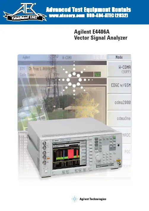
1981Agilent E4406AVector Signal AnalyzerAccuracyS p e e d2Fast and accurate measurements To stay competitive, wireless equipment manufacturers need flexible test equipment capable of testing different formats with little change in set-up. The Agilent E4406A vector signal analyzer (VSA) is the perfect fit, offering the best combination of speed and accuracy for making one-button,standards-based measurements.2.5G and 3G formatsFor engineers developing next-generation wireless components and systems, the E4406A provides W-CDMA, cdma2000,1xEV-DO and EDGE/GSM formats. Using one-button measurements, engineers can quickly verify conformance to these new formats. As the standards have evolved, we have continued to enhance existing measurement personalities, and add new ones. The modular architecture of the E4406A makes it simple for you to upgrade and be ready for the latest standards.You develop the wireless future…Easy to useMulti-format3…we provide the signal analysis.An investment for your future The number of wireless technologies deployed around the world is growing and the demand for any particular format can change quickly. The E4406A offers format and frequency flexibility.Comprehensive signal analysis Speeding up production means being ready to manufacture anything and lose no time doing it. The E4406A easily adapts to virtually any popular format:•W-CDMA •cdma2000•1xEV-DO •cdmaOne •EDGE •GSM •NADC •PDC •iDEN •Spectrum •Waveform“We have decreased the (transmitter power calibration)test time by 25%.”–T est Systems Designer4Built for speed…Fast standards-based measurements As a wireless system or componentmanufacturer, you are under pressure to increase throughput while minimizing capital investments. Long test times can severely limit your manufacturing throughput, so we designed the E4406A.Since its introduction, progressive enhancements to the E4406A ensure its performance keeps pace with the ever-increasing need for speed.Today's E4406A is faster than ever. For example, the W-CDMA adjacent channel power ratio (ACPR) measurement is now nearly eight times faster than it used to be.Output radio frequency spectrum (ORFS) is two times faster, W-CDMA code domain power (CDP) is five times faster, and other measurements have improved as well.The E4406A transmitter power calibration uses time record data and built-in algorithms to provide complete transmitter level calibration with incredible speed – with all the accuracy you expect from the affordably-priced E4406A.In addition to high-speed throughput and accuracy in the manufacturing environment,the E4406A is designed to allow research and development engineers to quickly obtain results with minimal keystrokes.The E4406A delivers a logical user interface and a wealth of quick “one button” measurments, enabling designers to quickly try multiple test without getting bogged down in crypitic menus. The E4406A interface provides the edge needed to expediently evaluate new designs and successfully meet the demands of today's competitive environment.Base station transceiver suite of testsTypical spectrum analyzerNow even faster…without giving up accuracy.Fast spectrum measurementsThe E4406A features pre-configured, one-button measurements for many cellular standards and can also be used for narrowband spectrum measurements. Manufacturers can expect to make inter-modulation distortion and other amplitude measurements up to three times faster using the E4406A. AccuracyYou don’t need to reduce measurementspeed to get accurate results. Superiorabsolute level accuracy of ±0.6 dB(±0.4 dB typical) provides unmatchedperformance and minimizes test uncertainty.Combined with a linearity of ±0.25 dBover a 76 dB range, the E4406A is astate-of-the-art measurement tool.Absolute level accuracyNarrow span spectrum measurement over GPIB E4406A VSA spectrum analyzer25 updates/second Typicalspectrumanalyzer56The E4406A VSA…Focused applications including EDGE, GSM,W-CDMA, cdma2000, 1xEV-DO, cdmaOne,and NADC as well as narrow-span spectrum and waveform analysisBaseband measurements with balanced/unbalanced multiple impedance inputsLarge,high-resolution, color display makes viewing multiple traces easyZoomfeature allows users to display selected measurement windowsAutomatic alignment ensures accurate measurement resultsOne-button,standards-based measurements7…comprehensive signal analysis.High-speed LAN, parallel, and GPIB ports provide speed and flexibility whenIntuitive key strokesBuilt-in floppy disk drive provides PC compatibility and data archivingManufacturing8Standards complianceIn manufacturing, you need straightforward pass/fail verification of critical specifications.With built-in test limits you don ’t have to keep track of every standard. The E4406A performs tests to the requirements of current industry standards with free, easy-to-install, firmware updates.Speed and throughputIn the world of high-speed manufacturing every millisecond counts. Identify your throughput restrictions and if measurement speed is creating a bottleneck, consider the significant speed advantage of the E4406A.Transmitter and receiver testingIn combination with the Agilent E4438C ESG vector signal generator, the E4406A offers base station receiver and transmitter testing for major 2G, 2.5G, and 3G wireless formats.The E4406A combined with an E4438C is a test solution that provides the required flexibility, without compromising accuracy, for maximum throughput in base station production with the ability to migrate to new formats.Designed for manufacturing…Development9Verify next-generation designs For R&D engineers developing next-generation wireless components and systems, the E4406A is a low-cost tool that quickly verifies conformance. Your investment is secure because the E4406A has a modular architecture – making it easy to upgrade to the latest standards.Characterize using leading test methodsDigital modulation presents new challenges to amplifier manufacturers.Designers need effective methods to quickly characterize digital signals. The E4406A ’s complementary cumulative-distribution function (CCDF) is useful for determining a signal ’s power statistics,revealing the power peaks relative to the average power for assessing linearity requirements.Flexible power measurements Multicarrier power amplifier (MCPA)designers are faced with new measurement challenges. Designers must characterize intermodulation distortion at many frequency offsets and evaluate the effects of different modulation formats over a wide dynamic range. The E4406A features a fully-configurable ACP measurement that can test up to five frequency offsets and be optimized for dynamic range or speed.…and product development.10GSM with EDGE (Option 202)The EDGE measurement personality performs the latest standards-based measurements, including:•Error vector magnitude (EVM)•Multi-slot power versus time (PvT)•ORFS •IQ offset•Channel plans for 400, 800, 900, 1800, 1900 MHz•GSM measurements from Option BAH The EVM measurement features a unique algorithm to simultaneously display the EVM numerical results and the EDGE constellation diagram using the industry-specified measurement filter.GSM (Option BAH)The GSM measurement personality lets you quickly perform measurements to the latest ETSI standards:•Mean transmitter carrier power •Multi-slot PvT •ORFS•Phase and frequency error (PFER)•IQ offset•Transmitter band spurious•Channel plans for 400, 700, 800, 900, 1800, 1900 MHzThe personality features easy channel and timeslot selections, configurable PvT masks,and a typical ORFS dynamic range of 90 dB.NADC and PDC (Option BAE)Both the North American Digital Cellular (NADC) and Personal Digital Cellular (PDC)measurement personalities are included in this option. The NADC measurements are structured according to the IS-136 TDMA standard. Measurements included in this option are:•ACP •EVM•Occupied bandwidth (for PDC)The personalities feature base station and mobile radio mode set-ups, as well as sync word search capability.iDEN (Option HN1)The iDEN measurement personality performs measurements to the Motorola iDEN specialized mobile radio format. •Occupied bandwidth (OBW)•ACPR•Transmitter bit error rate (BER)TDMA measurement personalities…11W-CDMA (Option BAF)The complexity of W-CDMA demands the flexibility and depth of demodulation capability provided by this personality.Perform the following measurements on the HPSK uplink or downlink QPSK signals:•Code domain •QPSK EVM•Modulation accuracy (composite rho and EVM)•Channel power•Adjacent channel power leakage ratio (ACLR)•Power control •PvT•Intermodulation distortion •Multicarrier power•Spectrum emission mask •OBW •CCDFThis personality has the ability toautomatically determine active channels,to synchronize with any W-CDMA channel,to display code domain power in a multi-rate view, and to demodulate down to the symbol level. Variable capture intervals and pre-defined test models enable the user to perform fast, accurate measurements for manufacturing or in-depth analysis for R&D.cdma2000 (Option B78)The cdma2000 measurement personality offers the logical upgrade path from IS-95 to IS-2000 testing. Measurements support the forward and reverse links.•Code domain •QPSK EVM•Modulation accuracy (composite rho and EVM)•Channel power •ACPR•Intermodulation distortion •Spectrum emission mask •OBW •CCDFAdvanced code domain analysis algorithms display Walch codes for either Hadamard or OVSF coding schemes in a multi-rate view. Other capability includes code domain power error, symbol EVM,symbol power versus time, active channel identification, variable PN offset, quasi-orthogonal functions and demodulated symbol bit displays after de-spreading.… and CDMA measurement personalities.12Expanding measurement potential…cdmaOne (Option BAC)Built on Agilent ’s pioneering efforts in CDMA measurement techniques,this personality provides quick and easy measurement set-ups for the TIA/EIA-95, J-STD-008,IS-97D, and IS-98D band classes:•Modulation accuracy (rho)•Code domain •Channel power •ACPR•Close-in spuriousAlong with the world ’s fastest ACPR measurements, this personality features PN (pseudo-noise sequence) search, time offset, and carrier feed-through analysis.1xEV-DO (Option 204)With digital demodulation analysis, the 1xEV-DO measurement personality provides the most comprehensive, easy-to-use,1xEV-DO measurement solution available in an analyzer. This personality, which performs measurements for both forward link and reverse link signals, provides key transmitter measurements for analyzing systems based on the 3GPP2 and TIA/EIA/IS-856 standards.Forward link•Channel power•Power versus time mask •Spurious emissions and ACP •Intermodulation distortion •OBW•Code domain•Modulation accuracy (composite rho)•QPSK EVM•Power statistics (CCDF)Reverse link •Code domain•Modulation accuracy (composite rho)For forward link, the PvT mask and spurious emissions/ACP measurements support both the idle slot (burst signal) and active slot (full power signal). With the auto-burst search function, you can see the standard-based time mask for the 1xEV-DO idle slot in PvT. Code domain, modulation accuracy (composite rho), and QPSK EVM can also measure for each channel ’s Pilot, MAC, and Data in QPSK/8PSK/16QAM. Designed with flexibility in mind, this personality supports the unique 1xEV-DO forward link signals ’feature of time divisions multiplex (TDM). For reverse link, code domain, and modulation accuracy provide powerful modulation analysis functions for transmitter tests.13IQ inputs (Option B7C)Capitalize on the E4406A ’s demodulation capabilities by extending the measurement range to baseband. The baseband IQ input option enables engineers to measure the complete signal path of a receiver or transmitter and directly compare signals both before and after frequency conversion and IQ (de)modulation.Ideally suited for R&D engineers and manufacturing environments, this option allows measurement of baseband I and Q signals in either balanced or unbalanced systems. Input configurations include 50-ohm unbalanced, 600-ohm balanced, and 1-Mohm balanced or unbalanced –enabling a variety of systems to be directly tested without cumbersome and error-inducing conversion networks.Applicable in-band 3GPP W-CDMA,cdma2000, EDGE/GSM, and Basic mode measurements are supported via RF and IQ inputs, enabling engineers to track down signal degradation both before and after RF/IF conversion.Additional features include auto calibration of input signals, variable dc offsets and a dc to 5-MHz input frequency range (10 MHz in I + jQ mode)....tailored to user requirements.14E4406A VSA/89601Asoftware combinationThe standards-based, one-button test capabilities of the E4406A can be expanded with the flexible digital demodulation and analysis capabilities of the Agilent 89601A PC software. This teaming provides fast and accurate data acquisition with powerful,flexible modulation analysis tools for, both common and evolving communications standards.The 89601A vector signal analysis software is the heart of the Agilent 89600 series of vector signal analyzers. This software provides flexible tools for demodulating and analyzing even the most advanced digital modulations, whether or not they are contained in an established standard. Features include variable block size signal acquisition with user-selectable pulse search and synch words, and a user-con-trollable adaptive equalizer. Filter types include cosine (raised and square-root raised), Gaussian, and low-pass – all with configurable alpha/BT. Supported modula-tion formats for both continuous and burst carriers include FSK (2, 4, 8, and 16 level),BPSK, QPSK, OQPSK, DQPSK, p/4DQPSK,8PSK, QAM (16 to 256 level), VSB (8 and 16 level), EDGE, and MSK.The software also provides signal capture and analysis features, such as the capability to download signal capture files for playback through signal generators,and display high-speed spectrograms.The 89601A software runs on a PC connected to the E4406A, via LAN or GPIB,and provides hardware control and results displays along with modulation analysis.Coupling speed and power…15/find/vsa…with Agilent’s tradition of excellence.Service and supportThe speed and accuracy of the E4406A VSA is only a small part of what you get from Agilent. We strive to provide complete solutions that go beyond our customers ’expectations. Only Agilent offers the depth and breadth of enhancements, software, services, connectivity, accessibility, and support to help you reach your measurement objectives. For more information on the E4406A VSA, including product and application literature, visit our Web site at /find/vsaPre-sales service• rentals, leasing, and financing • application engineering services Post-sales service• standard 3-year global warranty • Worldwide Call Center and Service Center support network • one-year calibration intervals • firmware upgrades downloadable from the Web PC connectivity • 10 baseT LAN port • floppy disk drive • GPIB interface• VXI Plug and Play driversPeripheral and product interfaces • parallel printer port • printer support • VGA monitor output• Agilent E4438C ESG vector signal generator•Agilent 89601A vector signal analysis softwareTraining and access to information • on-site user training • factory service training• Web-based support of frequently asked questions• manuals on CD-ROM and on the Web Software• programming examples on CD-ROM • SCPI (Standard Commands for Programmable Instruments)• PC-based performance verification and adjustment softwareOrdering Array informationE4406A vector signal analyzerModel DescriptionE4406A7 MHz to 4 GHzOption DescriptionDigital Demodulation MeasurementsE4406A-202EDGE with GSM measurementpersonalityE4406A-2041xEV-DO measurementpersonalityE4406A-B78cdma2000 measurementpersonalityE4406A-BAC cdmaOne measurementpersonalityE4406A-BAE NADC, PDC measurementpersonalityE4406A-BAF W-CDMA measurementpersonalityE4406A-BAH GSM measurement personality E4406A-HN1IDEN measurementpersonalityInputs and outputsE4406A-300321.4 MHz IF outputBBIQE4406A-B7C I/Q inputsCalibration documentationE4406A-UK6Commercial calibrationcertificate with test data AccessoriesE4406A-1CM Rack mount kitE4406A-1CN Handle kitE4406A-1CP Rack mount and handle kitE4406A-1CR Rack slide kit* Includes English manual set.。
Network Measurement1.At relative to 0 dBm output, 50 MHz,23 °C ±5 °C /HP-Agilent-4395A-Spectrum-Network-Analyzer.aspx To buy, sell, rent or trade-in this product please click on the link below:2Network MeasurementcontinuedReceiver CharacteristicsInput characteristicsFrequency range . . . . . . . . . . . . . . . . . . . . . . . . . . . . . . . . . . . . . . . . . . .10 Hz to 500 MHzInput attenuator . . . . . . . . . . . . . . . . . . . . . . . . . . . . . . . . . . . . . . . . .0 to 50 dB, 10 dB stepFull scale input level (R, A, B)Attenuator setting (dB) Full scale input level0–10 dBm100 dBm20+10 dBm30+20 dBm40+30 dBm50+30 dBmIF bandwidth (IFBW)2, 10, 30, 100, 300, 1 k, 3 k, 10 k, 30 kHzNote: The IFBW should be set to less than 1/5 of the lowest frequency inthe sweep range.Noise level (referenced to full scale input level, 23 °C ±5 °C)at 10 Hz ≤frequency < 100 Hz, IFBW = 2 Hz . . . . . . . . . . . . . . . . . . . . . .–85 dB (SPC)at 100 Hz ≤frequency < 100 kHz, IFBW = 10 Hz . . . . . . . . . . . . . . . . . . . . . . . . .–85 dBat 100 kHz ≤frequency, IFBW = 10 Hz . . . . . . . . . . . . . . . . . . . . . . . . . . . . . .-–115 dBInput crosstalkfor input R + 10 dBm input, input attenuator: . . . . . . . . . . . . . . . . . . . . . . . . . . . . .20 dBfor input A, B input attenuator: . . . . . . . . . . . . . . . . . . . . . . . . . . . . . . . . . . . . . . . . .0 dBat < 100 kHzR through A, B . . . . . . . . . . . . . . . . . . . . . . . . . . . . . . . . . . . . . . . . . . . . . .< –100 dBothers . . . . . . . . . . . . . . . . . . . . . . . . . . . . . . . . . . . . . . . . . . . . . . .< –100 dB (SPC)at ≥100 kHzR through A, B . . . . . . . . . . . . . . . . . . . . . . . . . . . . . . . . . . . . . . . . . . . . .< –120 dBothers . . . . . . . . . . . . . . . . . . . . . . . . . . . . . . . . . . . . . . . . . . . . . . .< –120 dB (SPC)Source crosstalk (for input A, B)(typical for input R)at + 10 dBm output, < 100 kHz, input attenuator: 0 dB . . . . . . . . . . . . . . . . .< –100 dBat + 10 dBm output, ≥100 kHz, input attenuator: 0 dB . . . . . . . . . . . . . . . . .< –120 dBMultiplexer switching impedance changeat input attenuator 0 dB . . . . . . . . . . . . . . . . . . . . . . . . . . . . . . . . . . . . . . . .< 0.5% (SPC)at input attenuator 10 dB and above . . . . . . . . . . . . . . . . . . . . . . . . . . . . . .< 0.1% (SPC)Connector . . . . . . . . . . . . . . . . . . . . . . . . . . . . . . . . . . . . . . . . . . . . . . . . . . . .Type-N femaleImpedance . . . . . . . . . . . . . . . . . . . . . . . . . . . . . . . . . . . . . . . . . . . . . . . . . . . .50 ΩnominalReturn lossInput attenuator0 dB10 dB20 dB to 50 dB10 Hz ≤frequency < 100 kHz25 dB125 dB125 dB1100 kHz ≤frequency ≤100 MHz25 dB125 dB25 dB1100 MHz < frequency15 dB115 dB15 dB1Maximum input level+30 dBm (at input attenuator: 40 dB or 50 dB)Maximum safe input level+30 dBm or ±7 Vdc (SPC)1.SPC34Absolute amplitude accuracy (R, A, B)at –10 dBm input, input attenuator:10 dB, frequency ≥100 Hz, IFBW ≤3 kHz, 23 °C ±5 °C, . . . . . . . . . . . .< ±1.5 dB Ratio accuracy (A/R, B/R) (typical for A/B)at –10 dBm input, input attenuator:10 dB, IFBW ≤3 kHz, 23 °C ±5 °C, . . . . . . . . . . . . . . . . . . . . . . . . . . . . . . .< ±2 dB Dynamic accuracy (A/R, B/R) (typical for A/B)Input level Dynamic accuracy 1(relative to full scale input level)frequency ≥100 Hz 0 dB ≥input level > –10 dB ±0.4 dB –10 dB ≥input Level ≥–60 dB ±0.05 dB –60 dB > input level ≥–80 dB ±0.3 dB –80 dB > input level ≥–100 dB ±3 dB Figure 1-1. Magnitude dynamic accuracy Residual responses . . . . . . . . . . . . . . . . . . . . . . . . . . . . . . . . . . .< –80 dB full scale (SPC)Trace noise (A/R, B/R, A/B)at 50 MHz, both inputs: full scale input level –10 dB, IFBW = 300 Hz . . . . . . . . . . . . . .< 0.005 dB rms (SPC)Stability (A/R, B/R, A/B) . . . . . . . . . . . . . . . . . . . . . . . . . . . . . . . .< ±0.01 dB/°C (SPC)Phase characteristics Measurements format . . . . . . . . . . . . . . . . . . .Standard format, expanded phase format Frequency response (deviation from linear phase) (A/R, B/R) (SPC for A/B) at –10 dBm input, input attenuator: 10 dB, IFBW ≤3 kHz, 23 °C ±5 °C . . . . . .< ±12°Dynamic accuracy (A/R, B/R) (SPC for A/B)Input level Dynamic accuracy 1(relative to full scale input level)frequency ≥100 Hz 0 dB ≥input level > –10 dB ±3°–10 dB ≥input Level ≥–60 dB ±0.3°–60 dB > input level ≥–80 dB ±1.8°–80 dB > input level ≥–100 dB ±18°Magnitude Characteristics1.R input level (B input level for A/B) = fullscale input level –10 dB, IFBW = 10 Hz,23 °C ± 5 °CInput level (dB)Magnitude dynamic accuracy D y n a m i c a c c u r a c y (d B )Spec Typical5Figure 1-2. Phase dynamic accuracyTrace noise (A/R, B/R, A/B)at 50 MHz, both inputs:full scale input level –10 dB, IFBW = 300 Hz . . . . . . . . . . . . . . . . .< 0.04°rms (SPC)Stability (A/R, B/R, A/B) . . . . . . . . . . . . . . . . . . . . . . . . . . . . . . . . . . .< ±0.1 °/°C (SPC)Group delay characteristicsAperture [Hz] . . . . . . . . . . . . . . . . . . . . . . . . . . . . . . . . . . . . . . . . . . .0.25% to 20% of span AccuracyIn general, the following formula can be used to determine the accuracy, in seconds,of a specific group delay measurement: . . . . . . . . . . . .Phase accuracy (degree)Aperture(Hz) x 360 (degree)Sweep characteristicsSweep type . . . . . . . . . . . . . . . . .Linear frequency, log frequency, power, list frequency Sweep direction . . . . . . . . . . . . . . . . . . . . . . . . . . . . . . . . . . . . . . . . . .Upper direction only Trigger type . . . . . . . . . . . . . . . . . . . . . . . . . .Hold, single, number of groups, continuous Trigger source . . . . . . . . . . . . . . . . . . . .Internal (free run), external, manual, GPIB (bus)Event trigger . . . . . . . . . . . . . . . . . . . . . . . . . . . . . . . . . . . . . . . . . . . . . .On point, on sweepInput level (dB)Phase dynamic accuracyD y n a m i c a c c u r a c y (d e g r e e )Spec Typical6Frequency characteristics Frequency range . . . . . . . . . . . . . . . . . . . . . . . . . . . . . . . . . . . . . . . . . . .10 Hz to 500 MHz Frequency readout accuracy . . . . . . . .±((freq readout [Hz ]) x (freq ref accuracy [1]) + RBW [Hz ] + SPAN [Hz ])) [Hz ]where NOP means number of display points NOP -1Frequency reference (Option 4395A-800)Accuracy at 23 °C ±5 °C, referenced to 23 °C . . . . . . . . . . . . . . . . . . . . . . . . . . . . .< ±5.5 ppm Aging . . . . . . . . . . . . . . . . . . . . . . . . . . . . . . . . . . . . . . . . . . . . .< ±2.5 ppm/year (SPC) Initial achievable accuracy . . . . . . . . . . . . . . . . . . . . . . . . . . . . . . . .< ±1.0 ppm (SPC) Temperature stability at 23 °C ±5 °C, referenced to 23 °C . . . . . . . . . . . . . . . . . . . . . . . . .< ±2 ppm (SPC) Precision frequency reference (Option 4395A-1D5) Accuracy at 0 °C to 40 °C, referenced to 23 °C . . . . . . . . . . . . . . . . . . . . . . . . . . .< ±0.13 ppm Aging . . . . . . . . . . . . . . . . . . . . . . . . . . . . . . . . . . . . . . . . . . . . . . . . .< ±0.l ppm/year (SPC)Initial achievable accuracy . . . . . . . . . . . . . . . . . . . . . . . . . . . . . . . . .< ±0.02 ppm (SPC)Temperature stability at 0 °C to 40 °C, referenced to 23 °C . . . . . . . . . . . . . . . . . . . . . . . .< ±0.01 ppm (SPC)Resolution bandwidth (RBW)Range 3 dB RBW at span > 0 . . . . . . . . . . . . . . . . . . . . . . . . . . . . . .1 Hz to 1 MHz, 1-3 step 3 dB RBW at span = 0 . . . . . . . . . . . .3 k, 5 k, 10 k, 20 k, 40 k, 100 k, 200 k, 400 k, 800 k, 1.5 M, 3 M, 5 MHz Selectivity (60 dB BW/3 dB BW)at span > 0 . . . . . . . . . . . . . . . . . . . . . . . . . . . . . . . . . . . . . . . . . . . . . . . . . . . . . . . .< 3Mode . . . . . . . . . . . . . . . . . . . . . . . . . . . . . . . . . . . . . . . . . . . . . . . . . . . . .Auto or manual Accuracy at span > 0 . . . . . . . . . . . . . . . . . . . . . . . . . . . . . . . . . . . . . . . . . . . . . . . . . . . .< ±10%at span = 0 . . . . . . . . . . . . . . . . . . . . . . . . . . . . . . . . . . . . . . . . . . . . . . . . . . . .< ±30%Video bandwidth (VBW)Range at span > 0 . . . . . . . . . . . . . . . .3 MHz to 3 MHz, 1-3 step, 0.003 ≤VBW/RBW ≤1Noise sidebands Offset from carrier Noise sidebands ≥1 kHz < –95 dBc/Hz ≥100 kHz < –108 dBc/Hz Figure 1-3. Noise sidebandsSpectrum Measurement Frequency offset [Hz]N o i s e s i d e b a n d [d B c /H z ]Spec Typical7Amplitude range . . . . . . . . . . . . . . . . . . . . . . . . . .displayed average noise level to +30 dBm Reference value setting range . . . . . . . . . . . . . . . . . . . . . . . . . . . . . .–100 dBm to +30 dBm Level accuracy at –20 dBm input, 50 MHz, input attenuator: 10 dB, 23 °C ±5 °C . . . . . . . . . . .< ±0.8 dB Frequency response at -20 dBm input, input attenuator: 10 dB, referenced to level at 50 MHz, 23 °C ±5 °C frequency ≥100 Hz . . . . . . . . . . . . . . . . . . . . . . . . . . . . . . . . . . . . . . . . . . . . . .< ±1.5 dB frequency < 100 Hz . . . . . . . . . . . . . . . . . . . . . . . . . . . . . . . . . . . . . . . . . . . . . .< ±1.3 dB Amplitude fidelity 1Log scale 2Range Amplitude fidelity (dB to reference input lever [dB][dB]0 to –30±0.05–30 to –40±0.07–40 to –50±0.15–50 to –60±0.35–60 to –70±0.8–70 to –80±1.8Linear scale 2 . . . . . . . . . . . . . . . . . . . . . . . . . . . . . . . . . . . . . . . . . . . . . . . . . . . . . . . . . . .< ±3%Displayed average noise level at reference value ≤–40 dBm, input attenuator: auto or 0 dB at frequency ≥1 kHz . . . . . . . . . . . . . . . . . . . . . . . . . . . . . . . . . . . . . . . . . . . .–120 dBm/Hz at ≥100 kHz . . . . . . . . . . . . . . . . . . . . . . . . . . . . . . . . . . . . . . . . . . . . . . . . . . .–133 dBm/Hz at ≥10 MHz . . . . . . . . . . . . . . . . . . . . . . . . . . . . .(–145 + frequency/100 MHz) dBm/Hz 3Figure 1-4. Typical displayed average noise level Amplitude Characteristics1.Fidelity shows an extent of nonlinearity referenced to the reference input level.2.RBW = 10 Hz, –20 dBm ≤reference value ≤+30 dBm, reference input level = full scale input level –10 dB, 23 ±5 °C3. At start frequency ≥10 MHzNote: Refer to Input attenuator part for the definition of full scale input level.Frequency offset [Hz]A v e r a g e n o i s e l e v e l [d B m /H z ]SpecTypical8Figure 1-5. Typical on-screen dynamic range (center: 100 MHz)Spurious responses Second harmonic distortion at single tone input with full scale input level –10 dB, input signal frequency ≥100 kHz . . . . . . . . . . . . . . . . . . . . . . . . . . . . . . . . . . . . . . . . . . .< –70 dBc, < –75 dBc (SPC)Third order inter-modulation distortion at two tones input with full scale input level –16 dB, separation ≥100 kHz . . . . . . . . . . . . . . . . . . . . . . . . . . . . . . . . . . . . . . . . . . . .< –75 dBc, < 80 dBc (SPC)Spurious at single tone input with full scale input level –10 dB, input signal frequency ≤500 MHz . . . . . . . . . . . . . . . . . . . . . . . . . . . . . . . . . . . . . . . . . . . . . . . . . . . . . . . . . .< –75 dBc except for the following frequency ranges:5.6 MHz ±1 MHz, 30.6 MHz ±1 MHz, 415.3 MHz ±1 MHz Residual response at reference value setting ≤–40 dBm, input attenuator: auto or 0 dB . . . . .< –110 dBmOn-screen Dynamic Range Offset frequency [Hz]O n -s c r e e n d y n a m i c r a n g e [d B c ]9Figure 1-6. Typical dynamic range at inputs R, A, and B Input attenuator Setting range . . . . . . . . . . . . . . . . . . . . . . . . . . . . . . . . . . . . . . . .0 dB to 50 dB, 10 dB step Attenuator setting (dB) Full scale input level 0–20 dBm 10–10 dBm 200 dBm 30+10 dBm 40+20 dBm 50+30 dBm Mode . . . . . . . . . . . . . . . . . . . . . . . . . . . . . . . . . . . . . . . . . . . . . . . . . . . . . . . . .Auto or manual (In auto mode, the attenuator is set to 20 dB above the reference value; this ensures that the maximum signal level after the attenuator will not be greater than –20 dBm.)Input attenuator switching uncertainty at attenuator: ≤30 dB, referenced to 10 dB . . . . . . . . . . . . . . . . . . . . . . . . . . . . .< ±1.0 dB at attenuator: ≥40 dB, referenced to 10 dB . . . . . . . . . . . . . . . . . . . . . . . . . . . .< ±1.5 dB Temperature drift . . . . . . . . . . . . . . . . . . . . . . . . . . . . . . . . . . . . . . . . . .< ±0.05 dB/°C (SPC)Scale Log 0.1 dB/div to 20 dB/div Linear at watt . . . . . . . . . . . . . . . . . . . . . . . . . . . . . . . . . . . . . . . . . . . . . . . . . . .1.0 x 10-12W/div at volt . . . . . . . . . . . . . . . . . . . . . . . . . . . . . . . . . . . . . . . . . . . . . . . . . . . . .1.0 x 10-9V/div Measurement format . . . . . . . . . . . . . . . . . . . . . . . . . . . . . . . . . . . . .Spectrum or noise (/Hz) Display unit . . . . . . . . . . . . . . . . . . . . . . . . . . . .dBm (unit of marker: dBm, dBV, dBµV, V, W)Sweep characteristics Sweep type . . . . . . . . . . . . . . . . . . . . . . . . . . . . . . . . . . . . . . . . . . . . . . . . . . . . . .Linear, list Trigger type . . . . . . . . . . . . . . . . . . . . . . . . . . .Hold, single, number of groups, continuous Trigger source . .Internal (free run), external, manual, level gate, edge gate, GPIB (bus)Sweep time (excluding each sweep setup time)RBW SPAN Typical sweep time 1 MHz 500 MHz 190 ms 100 kHz 100 MHz 300 ms 10 kHz 10 MHz 240 ms 1 kHz 1 MHz 190 ms 100 Hz 100 kHz 270 ms 10 Hz 10 kHz 2.0 s 1 Hz 1 kHz 11 s—Zero Span —1Typical Dynamic Range1.See the next item for sweep time at zero span Input level (dB)(Relative to full scale input level)D y n a m i c r a n g e (d B )Sensitivity (1 Hz RBW)Sensitivity ( 100 Hz RBW)2nd harmonic distortion 3rd order inter-modulation distortion Second Third1011Gate lengthRange . . . . . . . . . . . . . . . . . . . . . . . . . . . . . . . . . . . . . . . . . . . . . . . . . . . . . . .6 µs to 3.2 s ResolutionRange of gate length (T I )Resolution 6 µs ≤T I ≤25 ms 0.4 µs 25 ms < T I ≤64 ms 1 µs 64 ms < T I ≤130 ms 2 µs 130 ms < T I ≤320 ms 5 µs 320 ms < T I ≤1.28 s 20 µs 1.28s < T I ≤3.2 s100 µsGate lengthRange . . . . . . . . . . . . . . . . . . . . . . . . . . . . . . . . . . . . . . . . . . . . . . . . . . . . . . .2 µs to 3.2 sResolutionRange of gate delay (T d )Resolution 2 µs ≤T d ≤25 ms 0.4 µs 25 ms < T d ≤64 ms 1 µs 64 ms <T d ≤130 ms 2 µs 130 ms < T d ≤320 ms 5 µs 320 ms < T d ≤1.28 s 20 µs 1.28 s < T d ≤3.2 s100 µsAdditional amplitude errorLog scale . . . . . . . . . . . . . . . . . . . . . . . . . . . . . . . . . . . . . . . . . . . . . . . . . .< 0.3 dB (SPC)Linear scale . . . . . . . . . . . . . . . . . . . . . . . . . . . . . . . . . . . . . . . . . . . . . . . . . .< 3% (SPC)Gate control modes . . . . . . . . . . . . . . . . . . . . . . . . . . . . .Edge (positive/negative) or level Gate trigger input (external trigger input is used)Connector . . . . . . . . . . . . . . . . . . . . . . . . . . . . . . . . . . . . . . . . . . . . . . . . . . . .BNC female Level . . . . . . . . . . . . . . . . . . . . . . . . . . . . . . . . . . . . . . . . . . . . . . . . . . . . . . . . . . . . . . .TTL Gate outputConnector . . . . . . . . . . . . . . . . . . . . . . . . . . . . . . . . . . . . . . . . . . . . . . . . . . . .BNC female Level . . . . . . . . . . . . . . . . . . . . . . . . . . . . . . . . . . . . . . . . . . . . . . . . . . . . . . . . . . . . . . . .TTLSpecifications when Option 4395A-1D6 Time-Gated Spectrum Analysis is InstalledAll specifications are identical to the standard Agilent 4395A except the following items.12Measurement functions Measurement parameters Z, Y, L, C, Q, R, X, G, B, θDisplay parameters IZI, 0z , R, X, IYI, θy , G, B, I ΓI, θγ, Γx , Γy , Cp, Cs,Lp, Ls, Rp, Rs, D, QDisplay formats•Vertical lin/log scale •Complex plane•Polar/Smith/admittance chart Sweep parameters•Linear frequency sweep•Logarithmic frequency sweep •List frequency sweep•Power sweep (in dBm unit)IF bandwidth•2,10, 30, 100, 300, 1k, 3k, 10k, 30k [Hz]Calibration•OPEN/SHORT/LOAD 3 term calibration •Fixture compensation •Port extension correction Measurement port type •7-mm Output characteristicsFrequency range . . . . . . . . . . . . . . . . . . . . . . . . . . . . . . . . . . . . . . . . . .100 kHz to 500 MHz Frequency resolution . . . . . . . . . . . . . . . . . . . . . . . . . . . . . . . . . . . . . . . . . . . . . . . . .1 MHz Output impedance . . . . . . . . . . . . . . . . . . . . . . . . . . . . . . . . . . . . . . . . . . . . .50 Ωnominal Output levelwhen the measurement port is terminated by 50 Ω1 . . . . . . . . . . . . . .–56 to +9 dBm when the measurement port is open . . . . . . . . . . . . . . . . . . .0.71 mVrms to 1.26 Vrms Resolution . . . . . . . . . . . . . . . . . . . . . . . . . . . . . . . . . . . . . . . . . . . . . . . . . . . . . . . . . . .0.1 dBm Level accuracy . . . . . . . . . . . . . . . . . . . . . . . . . . . . . . . . . . . .±(A + B + 6 x F/(1.8 x 109))dB WhereA = 2 dBB = 0 dB (at 0 dBm ≤P ≤+ 15 dBm) or B = 1 dB (at –40 dBm ≤P < 0 dBm) or B = 2 dB (at –50 dBm ≤P < –40 dBm)F is setting frequency [Hz], P is output power settingOption 4395A-010Impedance measurementThe following specifications are applied when the 43961A impedance test kit is connected to the 4395A.1.When the measurement port is terminated with 50 Ω, the signal level at the measure-ment port is 6 dB lower than the signal level at the RF OUT port.13Measurement accuracy is specified at the connecting surface of the 7-mm connector of the Agilent 43961A under the following conditions:Warm up time . . . . . . . . . . . . . . . . . . . . . . . . . . . . . . . . . . . . . . . . . . . . . . . . .> 30 minutes Ambient temperature . . . . . . . . . . . . . . . . . . . . . . . . . . . . . . . . . . . . . . . . . . . .23 °C ±5 °C,within ±1 °C from the temperature at which calibration is performedSignal level (setting) . . . . . . . . . . . . . . . . . . . . . . . . . . . . . . . . . . . . . . . . . . .0 to +15 dBm Correction . . . . . . . . . . . . . . . . . . . . . . . . . . . . . . . . . . . . . . . . . . . . . . . . . . . . . . . . . . . . .ON IFBW (for calibration and measurement) . . . . . . . . . . . . . . . . . . . . . . . . . . . . . .≤300 Hz Averaging factor (for calibration and measurement) . . . . . . . . . . . . . . . . . . . . . . . . .≥8Figure 1-7. Impedance measurement accuracyIZI - θaccuracy IZI accuracy Z a = A + (B /I Z m I + C x I Z m I) x 100 [%]θaccuracy θa = sin -1(Z a /100)Where, I Z m I is I Z I measured. A, B, and C are obtained from Figure 1-7.IYI - θaccuracy IYI accuracy Y a = A + (B x I Y m I + C /I Z m I) x 100 [%]θaccuracy θa = sin -1(Y a /100)Where, I Y m I is I Y I measured. A, B, and C are obtained from Figure 1-7.Measurement Basic Accuracy(Supplemental performancecharacteristics)Test frequency [Hz]14Display LCDSize/type . . . . . . . . . . . . . . . . . . . . . . . . . . . . . . . . . . . . . . . . . . . . . . .8.4 inch color LCD Number of pixels . . . . . . . . . . . . . . . . . . . . . . . . . . . . . . . . . . . . . . . . . . . . . . . .640 x 480Effective display area . . . . . . . . . . . . . . . . . . . . . . .160 mm x 115 mm(600 x 430 dots)Number of display channels . . . . . . . . . . . . . . . . . . . . . . . . . . . . . . . . . . . . . . . . . . . . .2Format single, dual (split or overwrite)Number of traces . . . . . . . . . . . . . . . . . . . . . . . . . . . . . . . . . . . . . . . . . . . . . . . . . . . . . . . . . .For measurement . . . . . . . . . . . . . . . . . . . . . . . . . . . . . . . . . . . . . . . . . . . . . . . . .2 traces For memory . . . . . . . . . . . . . . . . . . . . . . . . . . . . . . . . . . . . . . . . . . . . . . . . . . . . . .2 traces Data math . . . . . . . . . . . . . . . . . . . . . . . . . . . . . . . . . . . . . . . . . . . . . . .gain x data – offset,gain x (data - memory) – offset,gain x (data + memory) – offset,gain x (data/memory ) – offsetData hold . . . . . . . . . . . . . . . . . . . . . . . . . . . . . . . . . . . . . . .Maximum hold, minimum hold MarkerNumber of markersMain marker . . . . . . . . . . . . . . . . . . . . . . . . . . . . . . . . . . . . . . . . . . . .l for each channel Sub-marker . . . . . . . . . . . . . . . . . . . . . . . . . . . . . . . . . . . . . . . . . . . . .7 for each channel ∆marker . . . . . . . . . . . . . . . . . . . . . . . . . . . . . . . . . . . . . . . . . . . . . . .1 for each channel Hard copyMode . . . . . . . . . . . . . . . . . . . . . . . . . . . .Dump mode only (including color dump mode)StorageBuilt-in flexible disk driveType . . . . . . . . . . . . . . . . . . . . . . . . . . . . . . . . . . . . . .3.5 inch, 1.44 MByte, or 720 KByte,1.44 MByte format is used for disk initializationMemory . . . . . . . . . . . . . . . . . . . . . . . . . . .512 KByte, can be backed up by flash memory GPIBInterface . . . . . . . . . . . . . . . . . . . . . . . . . . . . . . . . . . . . .IEEE 488.1-1987, IEEE 488.2-1987,IEC 625, and JIS C 1901-1987 standards compatible.Interface function . . . . . . . . . . . . . . . . . . . . . . . . .SH1, AH1, T6, TEO, L4, LEO, SR1, RL1,PP0, DC1, DT1, C1, C2, C3, C4, C11, E2Data transfer formats . . . . . . . . . . . . . . . . . . . . . . . . . . . . . . . . . . . . . . . . . . . . . . . . .ASCII,32 and 64 bit IEEE 754 floating point format,DOS PC format (32 bit IEEE with byte order reversed)Printer parallel portInterface . . . . . . . . . . . . . . . . . . . . . . . . . . . . . . .IEEE 1284 Centronics standard compliant Printer control language . . . . . . . . . . . . . . . . . . . . . . . . . . .PCL3 printer control language Connector . . . . . . . . . . . . . . . . . . . . . . . . . . . . . . . . . . . . . . . . . . . . . . . . . . .D-SUB (25-pin)15Common toNetwork/Spectrum/Impedance Measurement16Option 4395A-001 DC voltage/current sourceThe setting of Option 4395A-001 DC voltage/current source is independent of channel 1 and channel 2 settings.VoltageRange . . . . . . . . . . . . . . . . . . . . . . . . . . . . . . . . . . . . . . . . . . . . . . . . . . . . .–40 V to +40 V Resolution . . . . . . . . . . . . . . . . . . . . . . . . . . . . . . . . . . . . . . . . . . . . . . . . . . . . . . . . .1 mV Current limitationat voltage setting = –25 V to +25 V . . . . . . . . . . . . . . . . . . . . . . . . . . . . . .±100 mAat voltage setting = –40 V to –25 V, 25 V to 40 V . . . . . . . . . . . . . . . . . . .±20 mA CurrentRange–20 µA to -100 mA, 20 µA to 100 mAResolution . . . . . . . . . . . . . . . . . . . . . . . . . . . . . . . . . . . . . . . . . . . . . . . . . . . . . . . . . . .20 µA Voltage limitationat current setting = –20 mA to +20 mA . . . . . . . . . . . . . . . . . . . . . . . . . . . . . . .±40 V at current setting = –100 mA to –20 mA, 20 mA to 100 mA . . . . . . . . . . . . . .±25 V AccuracyVoltageat 23 °C ±5 °C . . . . . . . . . . . . . . . . . . . . . . .±(0.1% + 4 mV + I dc1[mA] x 5 [Ω] mV) Currentat 23 °C ±5 °C . . . . . . . . . . . . . . . . . . . . . . .±(0.5% + 30 µA + V dc2[V]/10 [kΩ] mA) Probe powerOutput voltage . . . . . . . . . . . . . . . . .+15 V (300 mA), –12.6 V (160 mA), GND nominal Specifications when instrument BASIC is operatedKeyboard . . . . . . . . . . . . . . . . . . . . . . . . . . . . . . . . . . . . .PS/2 style 101 English keyboard Connector . . . . . . . . . . . . . . . . . . . . . . . . . . . . . . . . . . . . . . . . . . . . . . . . . . . . . .mini-DIN 8 bit I/0 portConnector . . . . . . . . . . . . . . . . . . . . . . . . . . . . . . . . . . . . . . . . . . . . . . . . .D-SUB (15-pin) Level . . . . . . . . . . . . . . . . . . . . . . . . . . . . . . . . . . . . . . . . . . . . . . . . . . . . . . . . . . . . . . .TTL Number of input/output bit . . . . . . . . . . . . . . . . . . . . . .4 bit for input, 8 bit for outputFigure 1-8. 8 bit I/O port pin assignments24-bit I/O interfaceConnector . . . . . . . . . . . . . . . . . . . . . . . . . . . . . . . . . . . . . . . . . . . . . . . . . . .D-SUB (36-pin) Level . . . . . . . . . . . . . . . . . . . . . . . . . . . . . . . . . . . . . . . . . . . . . . . . . . . . . . . . . . . . . . . . .TTL I/O . . . . . . . . . . . . . . . . . . . . . . . . . . . . . . . . . . .8-bit for input or output, 16-bit for output Figure 1-9. 24-bit I/O interface pin assignment1.Current at DC source connector.2.Voltage at DC source connector.Table 1-1. Signal source assignmentPin No. Signal name Signal standard1GND0 V2INPUT1TTL level, pulse input (pulse width: 1 µs or above) 3OUTPUT1TTL level, latch output4OUTPUT2TTL level, latch output5OUTPUT PORT A0TTL level, latch output6OUTPUT PORT A1TTL level, latch output7OUTPUT PORT A2TTL level, latch output8OUTPUT PORT A3TTL level, latch output9OUTPUT PORT A4TTL level, latch output10OUTPUT PORT A5TTL level, latch output11OUTPUT PORT A6TTL level, latch output12OUTPUT PORT A7TTL level, latch output13OUTPUT PORT B0TTL level, latch output14OUTPUT PORT B1TTL level, latch output15OUTPUT PORT B2TTL level, latch output16OUTPUT PORT B3TTL level, latch output17OUTPUT PORT B4TTL level, latch output18OUTPUT PORT B5TTL level, latch output19OUTPUT PORT B6TTL level, latch output20OUTPUT PORT B7TTL level, latch output21I/O PORT C0TTL level, latch output22I/O PORT C1TTL level, latch output23I/O PORT C2TTL level, latch output24I/O PORT C3TTL level, latch output25I/O PORT D0TTL level, latch output26I/O PORT D1TTL level, latch output27I/O PORT D2TTL level, latch output28I/O PORT D3TTL level, latch output29PORT C STATUS TTL level, input mode: LOW, output mode: HIGH 30PORT D STATUS TTL level, input mode: LOW, output mode: HIGH 31WRITE STROBE SIGNAL TTL level, active low, pulse output(width: 10 µs; typical)32+5 V PULLUP33SWEEP END SIGNAL TTL level, active low, pulse output(width: 20 µs; typical)34+5 V+5 V, 100 mA MAX35PASS/FAIL SIGNAL TTL level, PASS: HIGH, FAIL: LOW, latch output36PASS/FAIL WRITE STROBE SIGNALTTL level, active low, pulse output(width: 10 µs; typical)1718Input and output characteristicsExternal reference inputFrequency . . . . . . . . . . . . . . . . . . . . . . . . . . . . . . . . . . . . . . . . . .10 MHz ±100 Hz (SPC)Level . . . . . . . . . . . . . . . . . . . . . . . . . . . . . . . . . . . . . . . . . . . . .-5 dBm to +5 dBm (SPC)Input impedance . . . . . . . . . . . . . . . . . . . . . . . . . . . . . . . . . . . . . . . . . . . . .50 Ωnominal Connector . . . . . . . . . . . . . . . . . . . . . . . . . . . . . . . . . . . . . . . . . . . . . . . . . . . .BNC female Internal reference outputFrequency . . . . . . . . . . . . . . . . . . . . . . . . . . . . . . . . . . . . . . . . . . . . . . . .10 MHz nominal Level . . . . . . . . . . . . . . . . . . . . . . . . . . . . . . . . . . . . . . . . . . . . . . . . . . . . . . .0 dBm (SPC)Output impedance . . . . . . . . . . . . . . . . . . . . . . . . . . . . . . . . . . . . . . . . . . .50 Ωnominal Connector . . . . . . . . . . . . . . . . . . . . . . . . . . . . . . . . . . . . . . . . . . . . . . . . . . . .BNC female Reference oven output (Option 4395A-1D5)Frequency . . . . . . . . . . . . . . . . . . . . . . . . . . . . . . . . . . . . . . . . . . . . . . . .10 MHz nominal Level . . . . . . . . . . . . . . . . . . . . . . . . . . . . . . . . . . . . . . . . . . . . . . . . . . . . . . .0 dBm (SPC)Output impedance . . . . . . . . . . . . . . . . . . . . . . . . . . . . . . . . . . . . . . . . . . .50 Ωnominal Connector . . . . . . . . . . . . . . . . . . . . . . . . . . . . . . . . . . . . . . . . . . . . . . . . . . . .BNC female External trigger inputLevel . . . . . . . . . . . . . . . . . . . . . . . . . . . . . . . . . . . . . . . . . . . . . . . . . . . . . . . . . . . . . . .TTL Pulse width (Tp) . . . . . . . . . . . . . . . . . . . . . . . . . . . . . . . . . . . . . . . . . . .≥2 µs typically Polarity . . . . . . . . . . . . . . . . . . . . . . . . . . . . . . . . . . . . . . . . .positive/negative selective Connector . . . . . . . . . . . . . . . . . . . . . . . . . . . . . . . . . . . . . . . . . . . . . . . . . . . .BNC female External program Run/Cont inputConnector . . . . . . . . . . . . . . . . . . . . . . . . . . . . . . . . . . . . . . . . . . . . . . . . . . . .BNC female Level . . . . . . . . . . . . . . . . . . . . . . . . . . . . . . . . . . . . . . . . . . . . . . . . . . . . . . . . . . . . . . .TTL Gate output (Option 4395A-1D6)Level . . . . . . . . . . . . . . . . . . . . . . . . . . . . . . . . . . . . . . . . . . . . . . . . . . . . . . . . . . . . . . .TTL Connector . . . . . . . . . . . . . . . . . . . . . . . . . . . . . . . . . . . . . . . . . . . . . . . . . . . .BNC femaleFigure 1-10. Trigger signal (external trigger input)General CharacteristicsPositive trigger signalNegative trigger signal。
Agilent MXA Signal Analyzer N9020AData SheetThe MXA signal analyzer takes signal and spectrum analysis to the next generation, offering the highest performance in a midrange signal analyzer with the industry’s fastest signal and spectrum analysis,eliminating the compromise between speed and performance. With a broad set of applications and demodulationcapabilities, an intuitive user interface,outstanding connectivity and powerful one-button measurements, the MXA is ideal for both R&D and manufacturing engineers working on cellular,emerging wireless communications,general purpose, aerospace and defense applications.Available frequency ranges N9020A-503 20 Hz to 3.6 GHz N9020A-50820 Hz to 8.4 GHz N9020A-513 20 Hz to 13.6 GHz N9020A-52620 Hz to 26.5 GHzFully LXI class C compliant2Definitions and ConditionsSpecifications describe the performance of parameters covered by the product warranty and apply over 5 to 50 °C unless otherwise noted. 95th percentile values indicate the breadth of the population (≈2σ) of performance tolerances expected to be metin 95 percent of the cases witha 95 percent confidence, for any ambient temperature in the range of 20 to 30 °C. In addition to the statistical observations of a sample of instruments, these values include the effects ofthe uncertainties of external calibration references. These values are not warranted. These values are updated occasionally if a significant change in the statistically observed behaviorof production instruments is observed. Typical describes additional product performance information that is not covered by the product warranty.It is performance beyond specifications that 80 percentof the units exhibit with a95 percent confidence level over the temperature range 20 to30°C. Typical performance does not include measurement uncertainty. Nominal values indicate expected performance, or describe product performance that is useful in the application of the product, but is not covered by the product warranty.The analyzer will meet itsspecifications when:•The analyzer is within itscalibration cycle.•Under auto couple control,except that Auto Sweep TimeRules = Accy.•For signal frequencies<20MHz, DC coupling applied.•The analyzer has been storedat an ambient temperaturewithin the allowed operatingrange for at least two hoursbefore being turned on, if ithad previously been storedat a temperature range insidethe allowed storage rangebut outside the allowedoperating range.•The analyzer has been turnedon at least 30 minutes withAuto Align set to normal, orif Auto Align is set to off orpartial, alignments must havebeen run recently enough toprevent an Alert message. Ifthe Alert condition is changedfrom Time and Temperature toone of the disabled durationchoices, the analyzer may failto meet specifications withoutinforming the user.This MXA signal analyzer datasheet is a summary of thecomplete specifications andconditions, which are availablein the MXA Signal AnalyzerSpecification Guide. The MXASignal Analyzer SpecificationGuide can be obtained on the webat: /find/mxa.Then follow this selectionprocess:•Select Technical Support underKey Library Information•Select Manuals and Guides•Download specifications guide3Frequency and Time Specifications456Amplitude Accuracy and Range Specifications78Dynamic Range Specifications10Figure 1. Nominal dynamic range – Band 0, for second and third order distortion, 20 Hz to 3.6 GHz Figure 2. Nominal dynamic range – Bands 1 to 4, second and third order distortion, 3.6 GHz to 26.5 GHzSecond harmonic distortion (SHI)Mixer level Distortion SHI10 MHz to 1.8 GHz–15 dBm–60 dBc+45 dBm1.8 to 7.0 GHz–15 dBm–80 dBc+65 dBm7.0 to 11.0 GHz–15 dBm–70 dBc+55 dBm11.0 to 13.25 GHz–15 dBm–65 dBc+50 dBm Preamp on (Option P03, P08, P13, P26)Preamp level Distortion SHI10 MHz to 1.8 GHz–45 dBm–75 dBc nominal+30 dBm nominal1.8 to 13.25 GHz–50 dBm–60 dBc nominal+10 dBmThird-order intermodulation distortion (TOI) (two –30 dBm tones at input mixer with tone separation > 15 kHz, 20 to 30 °C )Distortion TOI Typical10 to 100 MHz –84 dBc+12 dBm +17 dBm100 to 400 MHz –88 dBc+14 dBm +18 dBm400 MHz to 1.7 GHz –90 dBc+15 dBm +19 dBm1.7 to 3.6 GHz –92 dBc+16 dBm+19 dBm3.6 to 8.4 GHz –90 dBc+15 dBm+18 dBm8.4 to 13.6 GHz –90 dBc+15 dBm+18 dBm13.6 to 26.5 GHz –80 dBc+10 dBm+14 dBm Preamp on (Option P03, P08, P13, P26)10 MHz to 3.6 GHz20 dB lower than non-preamp mode, nominal(two –45 dBm tones at preamp input) 3.6 to 26.5 GHz35 dB lower than non-preamp mode, nominal, for offset <10 MHz3.6 to 26.5 GHz–14 dB, nominal, for offset >20 MHzPhase noise3Noise sidebands Offset Specification Typical(20 to 30 °C, CF = 1 GHz)100 Hz –80 dBc/Hz –86 dBc/Hz1 kHz –100 dBc/Hz nominal10 kHz –103 dBc/Hz –106 dBc/Hz100 kHz –115 dBc/Hz –117 dBc/Hz1 MHz –134 dBc/Hz –136 dBc/Hz10 MHz –147 dBc/Hz nominal 3For nominal values, refer to Figure 3.Figure 3. Nominal phase noise at different center frequencies (with Option PFR)Power Suite Measurement SpecificationsPower Suite Measurement Specifications (continued)General SpecificationsGeneral Specifications (continued)Input and OutputsInput and Outputs (continued)MXA Signal Analyzer Ordering InformationFor further information, refer to MXA Signal Analyzer Configuration Guide (5989-4943EN)Related LiteratureAgilent Technologies’ Test and Measurement Support, Services, and AssistanceAgilent Technologies aims to maximize the value you receive, while minimizing your risk and problems. We strive to ensure that you get the test and measurement capabilities you paid for and obtain the support you need. Our extensive support resources and services can help you choose the right Agilent products for your applications and apply them successfully.Every instrument and system we sell has a global warranty. Two concepts underlie Agilent’s overall support policy: “Our Promise” and “Your Advantage.”Our PromiseOur Promise means your Agilent test and measurement equipment will meet its advertised performance and functionality. When you are choosing new equipment, we will help you with product information, including realistic performance specifications and practical recommendations from experienced test engineers. When you receive your new Agilent equipment, we can help verify that it works properly and help with initial product operation.Your AdvantageYour Advantage means that Agilent offers a wide range of additional expert test and measurement services, which you can purchase according to your unique technical and business needs. Solve problems efficiently and gain a competitive edge by contracting with us for calibration, extra-cost upgrades, out-of-warranty repairs, and on-site education and training, as well as design, system integration, project management, and other professional engineering services. Experienced Agilent engineers and technicians worldwide can help you maximize your productivity, optimize the return on investment of your Agilent instruments and systems, and obtain dependable measurement accuracy for the life of those products.For more information on Agilent Technologies’products, applications or services, please contact your local Agilent office. The complete list is available at:/find/contactus Phone or Fax United States:(tel) 800 829 4444(fax) 800 829 4433Canada:(tel) 877 894 4414(fax) 800 746 4866China:(tel) 800 810 0189(fax) 800 820 2816Europe:(tel) 31 20 547 2111Japan:(tel) (81) 426 56 7832(fax) (81) 426 56 7840Korea:(tel) (080) 769 0800(fax) (080) 769 0900Latin America:(tel) (305) 269 7500Taiwan:(tel) 0800 047 866(fax) 0800 286 331Other Asia Pacific Countries:(tel) (65) 6375 8100(fax) (65) 6755 0042Email:*****************Contacts revised: 05/27/05Product specifications and descriptions in thisdocument subject to change without notice.© Agilent Technologies, Inc. 2006Printed in USA, August 31, 20065989-4942EN Agilent Email Updates/find/emailupdates Get the latest information on the products and applications you /find/mxa/find/agilentdirectQuickly choose and use your test equipment solutions with confidence.Agilent Open /find/open Agilent Open simplifies the process of connecting and programming test systems to help engineers design, validate and manufacture electronic products. Agilent offers open connectivity for a broad range of system-ready instruments, open industry software,PC-standard I/O and global support, which are combined to more easily integrate test system development.。

1981Agilent Technologies8510C Network AnalyzerOn-Site Service ManualSerial NumbersThis manual applies directly to instruments withthis serial prefix number or above: 3031A.Part Number:08510-90282Printed in USAMay 2012Supersedes: July 2003© Copyright Agilent Technologies 1994, 2001, 2003, 2012NoticeThe information contained in this document is subject to change without notice.Agilent Technologies makes no warranty of any kind with regard to this material, including, but not limited to, the implied warranties of merchantability and fitness for a particular purpose. Agilent Technologies shall not be liable for errors contained herein or for incidental or consequential damages in connection with the furnishing, performance, or use of this material.Agilent Technologies assumes no responsibility for the use or reliability of its software on equipment that is not furnished by Agilent Technologies.This document contains proprietary information which is protected by copyright. All rights are reserved. No part of this document may be photocopied, reproduced, or translated to another language without prior written consent of Agilent Technologies.Restricted Rights LegendUse, duplication, or disclosure by the U.S. Government is subject to restrictions as set forth in subparagraph (c)(1)(ii) of the Rights in Technical Data and Computer Software clause at DFARS 252.227-7013 for DOD agencies, and subparagraphs (c)(1) and (c)(2) of the Commercial Computer Software Restricted Rights clause at FAR 52.227-19 for other agencies.Documentation WarrantyTHE MATERIAL CONTAINED IN THIS DOCUMENT IS PROVIDED “AS IS,” AND IS SUBJECT TO BEING CHANGED, WITHOUT NOTICE, IN FUTURE EDITIONS. FURTHER, TO THE MAXIMUM EXTENT PERMITTED BY APPLICABLE LAW, AGILENT DISCLAIMS ALL WARRANTIES, EITHER EXPRESS OR IMPLIED WITH REGARD TO THIS MANUAL AND ANY INFORMATION CONTAINED HEREIN, INCLUDING BUT NOT LIMITED TO THE IMPLIED WARRANTIES OF MERCHANTABILITY AND FITNESS FOR A PARTICULAR PURPOSE. AGI-LENT SHALL NOT BE LIABLE FOR ERRORS OR FOR INCIDENTAL OR CONSEQUENTIAL DAMAGES IN CON-NECTION WITH THE FURNISHING, USE, OR PERFORMANCE OF THIS DOCUMENT OR ANY INFORMATION CONTAINED HEREIN. SHOULD AGILENT AND THE USER HAVE A SEPARATE WRITTEN AGREEMENT WITH WARRANTY TERMS COVERING THE MATERIAL IN THIS DOCUMENT THAT CONFLICT WITH THESE TERMS, THE WARRANTY TERMS IN THE SEPARATE AGREEMENT WILL CONTROL.Windows is a registered trademark of Microsoft Corporation.ii8510C On-Site Service Manua l8510C On-Site Service Manua l iiiContacting AgilentAny adjustment, maintenance, or repair of this product must be performed by qualified personnel. Contact Agilent by internet, phone, or fax to get assistance with all your test and measurement needs. Hewlett-Packard to Agilent Technologies TransitionThis manual may contain references to HP or Hewlett-Packard. Please note thatHewlett-Packard's former test and measurement, semiconductor products and chemical analysis businesses are now part of Agilent Technologies. To reduce potential confusion, the only change to product numbers and names has been in the company name prefix: where a product number/name was HP XXXX the current name/number is now Agilent XXXX. For example, model number HP478A is now model number Agilent 478A.Safety and Regulatory InformationReview this product and related documentation to familiarize yourself with safety markings and instructions Online assistance: /find/assistUnited States(tel)180****4844,or1 800 593-6635 for on-siteservice of systemsLatin America (tel) (305) 269 7500(fax) (305) 269 7599Canada (tel)187****4414(fax) (905) 282-6495Europe (tel) (+31) 20 547 2323(fax) (+31) 20 547 2390New Zealand(tel) 0 800 738 378(fax) (+64) 4 495 8950Japan (tel) (+81) 426 56 7832(fax) (+81) 426 56 7840Australia (tel) 1 800 629 485(fax) (+61) 3 9210 5947Singapore (tel)180****8100(fax) (65) 836 0252Malaysia(tel) 1 800 828 848(fax) 1 800 801 664Philippines (tel) (632) 8426802(tel) (PLDT subscriber only):1 800 16510170(fax) (632) 8426809(fax) (PLDT subscriber only):1 800 16510288Thailand (tel) outside Bangkok:(088) 226 008(tel) within Bangkok:(662) 661 3999(fax) (66) 1 661 3714Hong Kong (tel) 800 930 871(fax) (852) 2506 9233Taiwan (tel) 0800-047-866(fax) (886) 2 25456723People’s Republic of China(tel) (preferred): 800-810-0189(tel) (alternate):10800-650-0021(fax) 10800-650-0121India (tel) 1-600-11-2929(fax) 000-800-650-1101iv 8510C On-Site Service Manua lbefore you operate the instrument. This product has been designed and tested in accordance with international standards.WARNING The WARNING notice denotes a hazard. It calls attention to a procedure, practice,or the like, that, if not correctly performed or adhered to, could result in personal injury. Do not proceed beyond a WARNING notice until the indicated conditions are fully understood and met.CAUTIONThe CAUTION notice denotes a hazard. It calls attention to an operating procedure,practice, or the like, which, if not correctly performed or adhered to, could result indamage to the product or loss of important data. Do not proceed beyond a CAUTION notice until the indicated conditions are fully understood and met.Instrument MarkingsWhen you see this symbol on your instrument, you should refer to the instrument's instructionmanual for important information.This symbol indicates hazardous voltages.The C-tick is a registered trademark of the Australian Spectrum Management Agency.This symbol indicates that the instrument requires alternating current (ac) input.The CE mark is a registered trademark of the European Community. If it is accompanied by ayear, it indicates the year the design was proven.The CSA mark is a registered trademark of the Canadian Standards Association.ICES/NMB-001This ISM device complies with Canadian ICES-001.Cet appareil ISM est conforme a la norme NMB-001 du Canada.1SM1-A This text indicates that the instrument is an Industrial Scientific and Medical Group 1 Class Aproduct (CISPER 11, Clause 4).This symbol indicates that the power line switch is ON.This symbol indicates that the power line switch is OFF or in STANDBY position.Safety Earth GroundThis is a Safety Class I product (provided with a protective earthing terminal). An uninterruptible safety earth ground must be provided from the main power source to the product input wiring terminals, power cord, or supplied power cord set. Whenever it is likely that the protection has been impaired, the product must be made inoperative and secured against any unintended operation.Before Applying PowerVerify that the product is configured to match the available main power source as described in the input power configuration instructions in this manual. If this product is to be powered by autotransformer, make sure the common terminal is connected to the neutral (grounded) side of the ac power supply.Battery InformationThe 8510C uses a lithium poly carbon monoflouride battery to power the instrument clock. The battery is located on the A7 I/O board of the 85101C display/processor. This battery is not field replaceable. Replace the A7 I/O board if the battery requires replacement.WARNING Danger of explosion if battery is incorrectly replaced. Replace only with the same or equivalent type recommended. Discard used batteries according tomanufacturer’s instructions.8510C On-Site Service Manua l vTypeface ConventionsItalics•Used to emphasize important information:Use this software only with the Agilent Technologies xxxxxX system.•Used for the title of a publication:Refer to the Agilent Technologies xxxxxX System-Level User's Guide.•Used to indicate a variable:Type LOAD BIN filename.Instrument Display•Used to show on-screen prompts and messages that you will see on the display of an instrument: The Agilent Technologies xxxxxX will display the message CAL1SAVED.Keycap•Used for labeled keys on the front panel of an instrument or on acomputer keyboard:Press Return.[Softkey]•Used for simulated keys that appear on an instrument display:Press [Prior Menu].User Entry•Used to indicate text that you will enter using the computer keyboard; text shown in this typeface must be typed exactly as printed:Type LOAD PARMFILE•Used for examples of programming code:#endif//ifndef NO_CLASSPath name•Used for a subdirectory name or file path:Edit the file usr/local/bin/sample.txtComputer Display•Used to show messages, prompts, and window labels that appear on a computer monitor: The Edit Parameters window will appear on the screen.•Used for menus, lists, dialog boxes, and button boxes on a computer monitor from which you make selections using the mouse or keyboard:Double-click EXIT to quit the program.vi8510C On-Site Service Manua l1Service and EquipmentOverview . . . . . . . . . . . . . . . . . . . . . . . . . . . . . . . . . . . . . . . . . . . . . . . . . . . . . . . . . . . . . . . . . . . . . . . . . . . . . . . . . . . . . . .1-2 On-Site Service Manual Organization. . . . . . . . . . . . . . . . . . . . . . . . . . . . . . . . . . . . . . . . . . . . . . . . . . . . . . . . . . . . . . .1-3 Service and Equipment Overview (Chapter 1). . . . . . . . . . . . . . . . . . . . . . . . . . . . . . . . . . . . . . . . . . . . . . . . . . . . . .1-3 Safety/Licensing (Chapter 2). . . . . . . . . . . . . . . . . . . . . . . . . . . . . . . . . . . . . . . . . . . . . . . . . . . . . . . . . . . . . . . . . . . .1-3 Theory of Operation (Chapter 3) . . . . . . . . . . . . . . . . . . . . . . . . . . . . . . . . . . . . . . . . . . . . . . . . . . . . . . . . . . . . . . . . .1-3 Main Troubleshooting Procedure (Chapter 4). . . . . . . . . . . . . . . . . . . . . . . . . . . . . . . . . . . . . . . . . . . . . . . . . . . . . .1-3 Replaceable Parts (Chapter 5). . . . . . . . . . . . . . . . . . . . . . . . . . . . . . . . . . . . . . . . . . . . . . . . . . . . . . . . . . . . . . . . . . .1-4 Replacement Procedures (Chapter 6). . . . . . . . . . . . . . . . . . . . . . . . . . . . . . . . . . . . . . . . . . . . . . . . . . . . . . . . . . . . .1-4 Adjustments (Chapter 7) . . . . . . . . . . . . . . . . . . . . . . . . . . . . . . . . . . . . . . . . . . . . . . . . . . . . . . . . . . . . . . . . . . . . . . .1-4 Specifications and Performance Verification (Chapter 8). . . . . . . . . . . . . . . . . . . . . . . . . . . . . . . . . . . . . . . . . . . .1-4 Installation (Chapter 9). . . . . . . . . . . . . . . . . . . . . . . . . . . . . . . . . . . . . . . . . . . . . . . . . . . . . . . . . . . . . . . . . . . . . . . . .1-5 Preventive Maintenance (Chapter 10) . . . . . . . . . . . . . . . . . . . . . . . . . . . . . . . . . . . . . . . . . . . . . . . . . . . . . . . . . . . .1-5 Definition of an 8510 System. . . . . . . . . . . . . . . . . . . . . . . . . . . . . . . . . . . . . . . . . . . . . . . . . . . . . . . . . . . . . . . . . . . .1-5 Service Tools Available. . . . . . . . . . . . . . . . . . . . . . . . . . . . . . . . . . . . . . . . . . . . . . . . . . . . . . . . . . . . . . . . . . . . . . . . .1-5 Table of Service Equipment . . . . . . . . . . . . . . . . . . . . . . . . . . . . . . . . . . . . . . . . . . . . . . . . . . . . . . . . . . . . . . . . . . . . .1-6 2Safety/Licensing8510 Safety Information . . . . . . . . . . . . . . . . . . . . . . . . . . . . . . . . . . . . . . . . . . . . . . . . . . . . . . . . . . . . . . . . . . . . . . . . . .2-3 Hazardous Instrument Areas with Power On . . . . . . . . . . . . . . . . . . . . . . . . . . . . . . . . . . . . . . . . . . . . . . . . . . . . . .2-3 Compliance with German FTZ Emissions Requirements. . . . . . . . . . . . . . . . . . . . . . . . . . . . . . . . . . . . . . . . . . . . .2-6 Compliance with Canadian EMC Requirements. . . . . . . . . . . . . . . . . . . . . . . . . . . . . . . . . . . . . . . . . . . . . . . . . . . .2-6 3Theory of OperationOverview . . . . . . . . . . . . . . . . . . . . . . . . . . . . . . . . . . . . . . . . . . . . . . . . . . . . . . . . . . . . . . . . . . . . . . . . . . . . . . . . . . . . . . .3-2 The Base System. . . . . . . . . . . . . . . . . . . . . . . . . . . . . . . . . . . . . . . . . . . . . . . . . . . . . . . . . . . . . . . . . . . . . . . . . . . . . . . .3-3 Sources . . . . . . . . . . . . . . . . . . . . . . . . . . . . . . . . . . . . . . . . . . . . . . . . . . . . . . . . . . . . . . . . . . . . . . . . . . . . . . . . . . . . . . . .3-4 Synthesized Sweepers . . . . . . . . . . . . . . . . . . . . . . . . . . . . . . . . . . . . . . . . . . . . . . . . . . . . . . . . . . . . . . . . . . . . . . . . .3-4 Sweep Oscillators . . . . . . . . . . . . . . . . . . . . . . . . . . . . . . . . . . . . . . . . . . . . . . . . . . . . . . . . . . . . . . . . . . . . . . . . . . . . .3-4 Test Sets . . . . . . . . . . . . . . . . . . . . . . . . . . . . . . . . . . . . . . . . . . . . . . . . . . . . . . . . . . . . . . . . . . . . . . . . . . . . . . . . . . . . . . .3-5 Sampler-Based Test Sets . . . . . . . . . . . . . . . . . . . . . . . . . . . . . . . . . . . . . . . . . . . . . . . . . . . . . . . . . . . . . . . . . . . . . . .3-5 Mixer-Based Test Sets . . . . . . . . . . . . . . . . . . . . . . . . . . . . . . . . . . . . . . . . . . . . . . . . . . . . . . . . . . . . . . . . . . . . . . . . .3-5 8511 Frequency Converter . . . . . . . . . . . . . . . . . . . . . . . . . . . . . . . . . . . . . . . . . . . . . . . . . . . . . . . . . . . . . . . . . . . . . .3-5 Test Set Control Path. . . . . . . . . . . . . . . . . . . . . . . . . . . . . . . . . . . . . . . . . . . . . . . . . . . . . . . . . . . . . . . . . . . . . . . . . . .3-6 Test Set Power-On Sequence . . . . . . . . . . . . . . . . . . . . . . . . . . . . . . . . . . . . . . . . . . . . . . . . . . . . . . . . . . . . . . . . . . .3-6 Test Set Typical RF Path . . . . . . . . . . . . . . . . . . . . . . . . . . . . . . . . . . . . . . . . . . . . . . . . . . . . . . . . . . . . . . . . . . . . . . . .3-6 85102 IF/Detector . . . . . . . . . . . . . . . . . . . . . . . . . . . . . . . . . . . . . . . . . . . . . . . . . . . . . . . . . . . . . . . . . . . . . . . . . . . . . . .3-8 Signal Path Assemblies . . . . . . . . . . . . . . . . . . . . . . . . . . . . . . . . . . . . . . . . . . . . . . . . . . . . . . . . . . . . . . . . . . . . . . . .3-8 Control Assemblies. . . . . . . . . . . . . . . . . . . . . . . . . . . . . . . . . . . . . . . . . . . . . . . . . . . . . . . . . . . . . . . . . . . . . . . . . . . .3-9 Phase Lock Assemblies . . . . . . . . . . . . . . . . . . . . . . . . . . . . . . . . . . . . . . . . . . . . . . . . . . . . . . . . . . . . . . . . . . . . . . . .3-9 Miscellaneous Assemblies . . . . . . . . . . . . . . . . . . . . . . . . . . . . . . . . . . . . . . . . . . . . . . . . . . . . . . . . . . . . . . . . . . . . .3-9 85101 Display/Processor. . . . . . . . . . . . . . . . . . . . . . . . . . . . . . . . . . . . . . . . . . . . . . . . . . . . . . . . . . . . . . . . . . . . . . . .3-10 Processor Assemblies . . . . . . . . . . . . . . . . . . . . . . . . . . . . . . . . . . . . . . . . . . . . . . . . . . . . . . . . . . . . . . . . . . . . . . . .3-10 Display Assemblies (CRT) . . . . . . . . . . . . . . . . . . . . . . . . . . . . . . . . . . . . . . . . . . . . . . . . . . . . . . . . . . . . . . . . . . . . .3-10 Display Assemblies (LCD) . . . . . . . . . . . . . . . . . . . . . . . . . . . . . . . . . . . . . . . . . . . . . . . . . . . . . . . . . . . . . . . . . . . . .3-11 Input/Output Assemblies. . . . . . . . . . . . . . . . . . . . . . . . . . . . . . . . . . . . . . . . . . . . . . . . . . . . . . . . . . . . . . . . . . . . . .3-11 Power Supply . . . . . . . . . . . . . . . . . . . . . . . . . . . . . . . . . . . . . . . . . . . . . . . . . . . . . . . . . . . . . . . . . . . . . . . . . . . . . . . .3-12 8510 Typical System Measurement Sequence . . . . . . . . . . . . . . . . . . . . . . . . . . . . . . . . . . . . . . . . . . . . . . . . . . . . . .3-15 8510C On-Site Service ManualContents-1System Phase Lock Operation. . . . . . . . . . . . . . . . . . . . . . . . . . . . . . . . . . . . . . . . . . . . . . . . . . . . . . . . . . . . . . . . . . . .3-16 Pretune Phase Lock Sequence . . . . . . . . . . . . . . . . . . . . . . . . . . . . . . . . . . . . . . . . . . . . . . . . . . . . . . . . . . . . . . . . .3-16 Pretune IF Count Sequence . . . . . . . . . . . . . . . . . . . . . . . . . . . . . . . . . . . . . . . . . . . . . . . . . . . . . . . . . . . . . . . . . . . .3-18 Main Phase Lock Sequence. . . . . . . . . . . . . . . . . . . . . . . . . . . . . . . . . . . . . . . . . . . . . . . . . . . . . . . . . . . . . . . . . . . .3-19 Monitoring Phase Lock. . . . . . . . . . . . . . . . . . . . . . . . . . . . . . . . . . . . . . . . . . . . . . . . . . . . . . . . . . . . . . . . . . . . . . . .3-19 Monitoring the VTO. . . . . . . . . . . . . . . . . . . . . . . . . . . . . . . . . . . . . . . . . . . . . . . . . . . . . . . . . . . . . . . . . . . . . . . . . . .3-20 Phase Lock Learn Mode. . . . . . . . . . . . . . . . . . . . . . . . . . . . . . . . . . . . . . . . . . . . . . . . . . . . . . . . . . . . . . . . . . . . . . .3-20 Phase Lock Cycle Summary (Including Running Error Messages) . . . . . . . . . . . . . . . . . . . . . . . . . . . . . . . . . . . . .3-21 4Main Troubleshooting ProcedureOverview . . . . . . . . . . . . . . . . . . . . . . . . . . . . . . . . . . . . . . . . . . . . . . . . . . . . . . . . . . . . . . . . . . . . . . . . . . . . . . . . . . . . . . .4-2 Troubleshooting Outline . . . . . . . . . . . . . . . . . . . . . . . . . . . . . . . . . . . . . . . . . . . . . . . . . . . . . . . . . . . . . . . . . . . . . . . . . .4-3 What’s Wrong . . . . . . . . . . . . . . . . . . . . . . . . . . . . . . . . . . . . . . . . . . . . . . . . . . . . . . . . . . . . . . . . . . . . . . . . . . . . . . . .4-4Self Test Failures. . . . . . . . . . . . . . . . . . . . . . . . . . . . . . . . . . . . . . . . . . . . . . . . . . . . . . . . . . . . . . . . . . . . . . . . . . . .4-4Running Error Messages . . . . . . . . . . . . . . . . . . . . . . . . . . . . . . . . . . . . . . . . . . . . . . . . . . . . . . . . . . . . . . . . . . . . .4-6Unratioed Power Failures. . . . . . . . . . . . . . . . . . . . . . . . . . . . . . . . . . . . . . . . . . . . . . . . . . . . . . . . . . . . . . . . . . . . .4-6Other Obvious Failure Types . . . . . . . . . . . . . . . . . . . . . . . . . . . . . . . . . . . . . . . . . . . . . . . . . . . . . . . . . . . . . . . . . .4-6 Control, Configuration, and Cabling Pre-Operational Checks. . . . . . . . . . . . . . . . . . . . . . . . . . . . . . . . . . . . . . . . .4-8Front and Rear Panel Checks . . . . . . . . . . . . . . . . . . . . . . . . . . . . . . . . . . . . . . . . . . . . . . . . . . . . . . . . . . . . . . . . .4-8Cabling Checks . . . . . . . . . . . . . . . . . . . . . . . . . . . . . . . . . . . . . . . . . . . . . . . . . . . . . . . . . . . . . . . . . . . . . . . . . . . . .4-8Firmware Revisions. . . . . . . . . . . . . . . . . . . . . . . . . . . . . . . . . . . . . . . . . . . . . . . . . . . . . . . . . . . . . . . . . . . . . . . . .4-12 No Obvious Failure Type. . . . . . . . . . . . . . . . . . . . . . . . . . . . . . . . . . . . . . . . . . . . . . . . . . . . . . . . . . . . . . . . . . . . . . .4-20Verify the 85101C Display/Processor . . . . . . . . . . . . . . . . . . . . . . . . . . . . . . . . . . . . . . . . . . . . . . . . . . . . . . . . .4-20Verify the 85102 IF/Detector. . . . . . . . . . . . . . . . . . . . . . . . . . . . . . . . . . . . . . . . . . . . . . . . . . . . . . . . . . . . . . . . .4-20 Hardware Emulator Tools. . . . . . . . . . . . . . . . . . . . . . . . . . . . . . . . . . . . . . . . . . . . . . . . . . . . . . . . . . . . . . . . . . . . . .4-22Test Set Emulator . . . . . . . . . . . . . . . . . . . . . . . . . . . . . . . . . . . . . . . . . . . . . . . . . . . . . . . . . . . . . . . . . . . . . . . . . .4-22Source Emulator . . . . . . . . . . . . . . . . . . . . . . . . . . . . . . . . . . . . . . . . . . . . . . . . . . . . . . . . . . . . . . . . . . . . . . . . . . .4-22Other Tests for the Source. . . . . . . . . . . . . . . . . . . . . . . . . . . . . . . . . . . . . . . . . . . . . . . . . . . . . . . . . . . . . . . . . . .4-22 8510C System-Level Troubleshooting Block Diagram. . . . . . . . . . . . . . . . . . . . . . . . . . . . . . . . . . . . . . . . . . . . . .4-25 8510C System-Level Troubleshooting Block Diagram (LCD) . . . . . . . . . . . . . . . . . . . . . . . . . . . . . . . . . . . . . . . .4-27 8510C Display/Processor Overall Block Diagram (CRT) . . . . . . . . . . . . . . . . . . . . . . . . . . . . . . . . . . . . . . . . . . . .4-29 85101C Display/Processor Overall Block Diagram (LCD). . . . . . . . . . . . . . . . . . . . . . . . . . . . . . . . . . . . . . . . . . .4-31 85102C IF/Detector Overall Block Diagram . . . . . . . . . . . . . . . . . . . . . . . . . . . . . . . . . . . . . . . . . . . . . . . . . . . . . .4-33 8510C Phase Lock Block Diagram. . . . . . . . . . . . . . . . . . . . . . . . . . . . . . . . . . . . . . . . . . . . . . . . . . . . . . . . . . . . . . .4-35 85101C A8 Motherboard Wiring Diagram (CRT) (1 of 2) . . . . . . . . . . . . . . . . . . . . . . . . . . . . . . . . . . . . . . . . . . . .4-37 85101C A8 Motherboard Wiring Diagram (CRT) (2 of 2) . . . . . . . . . . . . . . . . . . . . . . . . . . . . . . . . . . . . . . . . . . . .4-38 85101C A8 Motherboard Wiring Diagram (LCD) (1 of 2) . . . . . . . . . . . . . . . . . . . . . . . . . . . . . . . . . . . . . . . . . . . .4-39 85101C A8 Motherboard Wiring Diagram (LCD) (2 of 2) . . . . . . . . . . . . . . . . . . . . . . . . . . . . . . . . . . . . . . . . . . . .4-40 85102C A8 Motherboard Wiring Diagram (1 of 2). . . . . . . . . . . . . . . . . . . . . . . . . . . . . . . . . . . . . . . . . . . . . . . . . .4-41 85102C A8 Motherboard Wiring Diagram (2 of 2). . . . . . . . . . . . . . . . . . . . . . . . . . . . . . . . . . . . . . . . . . . . . . . . . .4-42 LCD Failures . . . . . . . . . . . . . . . . . . . . . . . . . . . . . . . . . . . . . . . . . . . . . . . . . . . . . . . . . . . . . . . . . . . . . . . . . . . . . . . . . . .4-43 A14 GSP Display Interface Board . . . . . . . . . . . . . . . . . . . . . . . . . . . . . . . . . . . . . . . . . . . . . . . . . . . . . . . . . . . . . . .4-44 A15 LCD. . . . . . . . . . . . . . . . . . . . . . . . . . . . . . . . . . . . . . . . . . . . . . . . . . . . . . . . . . . . . . . . . . . . . . . . . . . . . . . . . . . . .4-46Troubleshooting Image Problems. . . . . . . . . . . . . . . . . . . . . . . . . . . . . . . . . . . . . . . . . . . . . . . . . . . . . . . . . . . . .4-46A16 Backlight Inverter Board . . . . . . . . . . . . . . . . . . . . . . . . . . . . . . . . . . . . . . . . . . . . . . . . . . . . . . . . . . . . . . . .4-49 Self Test Failures . . . . . . . . . . . . . . . . . . . . . . . . . . . . . . . . . . . . . . . . . . . . . . . . . . . . . . . . . . . . . . . . . . . . . . . . . . . . . . .4-51 Overview . . . . . . . . . . . . . . . . . . . . . . . . . . . . . . . . . . . . . . . . . . . . . . . . . . . . . . . . . . . . . . . . . . . . . . . . . . . . . . . . . . . .4-51 Self Tests and Other Failures. . . . . . . . . . . . . . . . . . . . . . . . . . . . . . . . . . . . . . . . . . . . . . . . . . . . . . . . . . . . . . . . . . .4-52What to Do If an Instrument Error Occurs. . . . . . . . . . . . . . . . . . . . . . . . . . . . . . . . . . . . . . . . . . . . . . . . . . . . . .4-52 Contents-28510C On-Site Service ManualWhat to Do If the R-L-T-S-8-4-2-1 LEDs Stay Lit (Default Test 15) . . . . . . . . . . . . . . . . . . . . . . . . . . . . . . . . .4-53Self Test Sequence . . . . . . . . . . . . . . . . . . . . . . . . . . . . . . . . . . . . . . . . . . . . . . . . . . . . . . . . . . . . . . . . . . . . . . . . .4-53How to Identify a Self Test Failure . . . . . . . . . . . . . . . . . . . . . . . . . . . . . . . . . . . . . . . . . . . . . . . . . . . . . . . . . . . .4-55How to Troubleshoot a Self Test Failure . . . . . . . . . . . . . . . . . . . . . . . . . . . . . . . . . . . . . . . . . . . . . . . . . . . . . . .4-58How to Access the Test Menu and Run a Self Test. . . . . . . . . . . . . . . . . . . . . . . . . . . . . . . . . . . . . . . . . . . . . .4-58Self Test Failures and Troubleshooting . . . . . . . . . . . . . . . . . . . . . . . . . . . . . . . . . . . . . . . . . . . . . . . . . . . . . . . .4-60 System, Disc, and Service Commands. . . . . . . . . . . . . . . . . . . . . . . . . . . . . . . . . . . . . . . . . . . . . . . . . . . . . . . . . . .4-65System Command 15: Run Main Program. . . . . . . . . . . . . . . . . . . . . . . . . . . . . . . . . . . . . . . . . . . . . . . . . . . . . .4-65System Command 16: Memory Operations. . . . . . . . . . . . . . . . . . . . . . . . . . . . . . . . . . . . . . . . . . . . . . . . . . . . .4-65System Command 17: Rerun Self Test. . . . . . . . . . . . . . . . . . . . . . . . . . . . . . . . . . . . . . . . . . . . . . . . . . . . . . . . .4-65System Command 18: Repeat Test Loop. . . . . . . . . . . . . . . . . . . . . . . . . . . . . . . . . . . . . . . . . . . . . . . . . . . . . . .4-65Disc Command 19: Load Program Disc . . . . . . . . . . . . . . . . . . . . . . . . . . . . . . . . . . . . . . . . . . . . . . . . . . . . . . . .4-65Disc Command 20: Record Program Disc . . . . . . . . . . . . . . . . . . . . . . . . . . . . . . . . . . . . . . . . . . . . . . . . . . . . . .4-66Disc Command 21: Initialize Disc . . . . . . . . . . . . . . . . . . . . . . . . . . . . . . . . . . . . . . . . . . . . . . . . . . . . . . . . . . . . .4-66Service Command 22: Run Service Program. . . . . . . . . . . . . . . . . . . . . . . . . . . . . . . . . . . . . . . . . . . . . . . . . . . .4-66Service Command 23: Diagnose a Failure. . . . . . . . . . . . . . . . . . . . . . . . . . . . . . . . . . . . . . . . . . . . . . . . . . . . . .4-66 How to Reload the Operating System . . . . . . . . . . . . . . . . . . . . . . . . . . . . . . . . . . . . . . . . . . . . . . . . . . . . . . . . . . .4-67 Running Error Messages . . . . . . . . . . . . . . . . . . . . . . . . . . . . . . . . . . . . . . . . . . . . . . . . . . . . . . . . . . . . . . . . . . . . . . . .4-69 Running Error Messages as Built-In Diagnostics. . . . . . . . . . . . . . . . . . . . . . . . . . . . . . . . . . . . . . . . . . . . . . . . . .4-69 Different Types of Running Error Messages . . . . . . . . . . . . . . . . . . . . . . . . . . . . . . . . . . . . . . . . . . . . . . . . . . . . . .4-69 Error Message Characteristics . . . . . . . . . . . . . . . . . . . . . . . . . . . . . . . . . . . . . . . . . . . . . . . . . . . . . . . . . . . . . . . . .4-70Caution Type Messages. . . . . . . . . . . . . . . . . . . . . . . . . . . . . . . . . . . . . . . . . . . . . . . . . . . . . . . . . . . . . . . . . . . . .4-70Prompt Type Messages . . . . . . . . . . . . . . . . . . . . . . . . . . . . . . . . . . . . . . . . . . . . . . . . . . . . . . . . . . . . . . . . . . . . .4-70Tell Type Messages. . . . . . . . . . . . . . . . . . . . . . . . . . . . . . . . . . . . . . . . . . . . . . . . . . . . . . . . . . . . . . . . . . . . . . . . .4-70Error Type Messages . . . . . . . . . . . . . . . . . . . . . . . . . . . . . . . . . . . . . . . . . . . . . . . . . . . . . . . . . . . . . . . . . . . . . . .4-70 Things to Remember about Running Error Messages. . . . . . . . . . . . . . . . . . . . . . . . . . . . . . . . . . . . . . . . . . . . . .4-71 Categories of Caution Running Error Messages. . . . . . . . . . . . . . . . . . . . . . . . . . . . . . . . . . . . . . . . . . . . . . . . . . .4-71Phase Lock Running Error Messages . . . . . . . . . . . . . . . . . . . . . . . . . . . . . . . . . . . . . . . . . . . . . . . . . . . . . . . . .4-71IF/Detector ADC Running Error Messages. . . . . . . . . . . . . . . . . . . . . . . . . . . . . . . . . . . . . . . . . . . . . . . . . . . . .4-71Source Sweep Running Error Messages. . . . . . . . . . . . . . . . . . . . . . . . . . . . . . . . . . . . . . . . . . . . . . . . . . . . . . .4-71GPIB (HP-IB) Running Error Messages. . . . . . . . . . . . . . . . . . . . . . . . . . . . . . . . . . . . . . . . . . . . . . . . . . . . . . . .4-71 Running Error Message Troubleshooting . . . . . . . . . . . . . . . . . . . . . . . . . . . . . . . . . . . . . . . . . . . . . . . . . . . . . . . .4-72System-Level Troubleshooting Block Diagram. . . . . . . . . . . . . . . . . . . . . . . . . . . . . . . . . . . . . . . . . . . . . . . . . .4-72Helpful Troubleshooting Hints. . . . . . . . . . . . . . . . . . . . . . . . . . . . . . . . . . . . . . . . . . . . . . . . . . . . . . . . . . . . . . . .4-72 Alphabetical List of Caution Running Error Messages . . . . . . . . . . . . . . . . . . . . . . . . . . . . . . . . . . . . . . . . . . . . .4-73ADC Cal Failed. . . . . . . . . . . . . . . . . . . . . . . . . . . . . . . . . . . . . . . . . . . . . . . . . . . . . . . . . . . . . . . . . . . . . . . . . . . . .4-73ADC Not Responding . . . . . . . . . . . . . . . . . . . . . . . . . . . . . . . . . . . . . . . . . . . . . . . . . . . . . . . . . . . . . . . . . . . . . . .4-73Autorange Cal Failed . . . . . . . . . . . . . . . . . . . . . . . . . . . . . . . . . . . . . . . . . . . . . . . . . . . . . . . . . . . . . . . . . . . . . . .4-74Caution: Optional Function Not Installed . . . . . . . . . . . . . . . . . . . . . . . . . . . . . . . . . . . . . . . . . . . . . . . . . . . . . .4-74Disc Communication Error. . . . . . . . . . . . . . . . . . . . . . . . . . . . . . . . . . . . . . . . . . . . . . . . . . . . . . . . . . . . . . . . . . .4-74Disc Hardware Problem. . . . . . . . . . . . . . . . . . . . . . . . . . . . . . . . . . . . . . . . . . . . . . . . . . . . . . . . . . . . . . . . . . . . .4-74Disc Read or Write Error . . . . . . . . . . . . . . . . . . . . . . . . . . . . . . . . . . . . . . . . . . . . . . . . . . . . . . . . . . . . . . . . . . . .4-74Disc Media Wearing Out - Replace Soon . . . . . . . . . . . . . . . . . . . . . . . . . . . . . . . . . . . . . . . . . . . . . . . . . . . . . .4-75Failure - Check System Bus Configuration . . . . . . . . . . . . . . . . . . . . . . . . . . . . . . . . . . . . . . . . . . . . . . . . . . . . .4-75Failure - Fault Indicator On . . . . . . . . . . . . . . . . . . . . . . . . . . . . . . . . . . . . . . . . . . . . . . . . . . . . . . . . . . . . . . . . . .4-75Failure - Overmodulation . . . . . . . . . . . . . . . . . . . . . . . . . . . . . . . . . . . . . . . . . . . . . . . . . . . . . . . . . . . . . . . . . . . .4-75Failure - RF Unlocked . . . . . . . . . . . . . . . . . . . . . . . . . . . . . . . . . . . . . . . . . . . . . . . . . . . . . . . . . . . . . . . . . . . . . . .4-75Failure - Self Test Failure . . . . . . . . . . . . . . . . . . . . . . . . . . . . . . . . . . . . . . . . . . . . . . . . . . . . . . . . . . . . . . . . . . . .4-75IF Cal Failed . . . . . . . . . . . . . . . . . . . . . . . . . . . . . . . . . . . . . . . . . . . . . . . . . . . . . . . . . . . . . . . . . . . . . . . . . . . . . . .4-758510C On-Site Service ManualContents-3。
安捷伦网络分析仪10 Gigabit 以太网分析解决方案有线协议测试-能够快速解决当前复杂网络问题的卓越技术网络分析仪软件使网络技术人员可以快速维护和优化下一代网络的话音业务和数据业务。
此外,任何人通过这些软件都可随时随地访问几乎任何网络,运行任何协议,从而降低运营成本,加速网络故障的诊断和排除过程。
安捷伦经验证的网络故障诊断解决方案添加了对 10 Gigabit 以太网的支持,可帮助您实现并超越您的客户满意度目标。
它将显著缩短启动时间,节省培训成本,使技术人员更快地解决更多网络问题。
网络分析仪在易于使用的 A gilent 10 GigE 网络分析仪上运行,轻松实现性能突破:功能-以 10 G b p s 速率捕获 100% 的网络流量。
高级以太网包捕获和处理功能意味着您将不会放过任何网络问题。
宽度-广泛的数据测量和话音测量,包括完整的协议分析,为您做出有效决定提供正确信息。
深度-高级数据包分析和统计,包括抖动、丢包和时延,广泛的前端捕获过滤以及远程控制,确保您在第一时间解决问题。
网络分析仪和 J6872A 10 GigE 接口共同组成了专家级网络测试和故障诊断解决方案,可在任何以太网 10/100/1000 Mbps 和 10 Gigabit 环境中提供实时测量。
安捷伦的网络分析仪解决方案按照问题严重性对故障进行优先级排序,确保对故障进行快速隔离。
广泛的有线协议测试功能包括:• 测试 10 Gigabit 以太网接口或 10/100/1000 Mbps 以太网接口• 协同专家分析仪软件,快速有效地解决网络问题• 使用性能统计和关键参数预测网络问题• 分析关键的全双工服务器或骨干网链路• 获得全面的网络统计• 对所有 7 层 OSI 上的 500 多种协议进行解码• 在 IPv4 和 IPv6 (或 IPv6 和 IPv4 混合) 环境中进行测试• 图形用户界面便于用户轻松浏览• 在 10 Gbps 链路或 10/100/1000 Mbps 以太网链路上生成 LAN 流量• 分析 MPLS ,对聚合网络进行故障诊断• J6865A 是一个用于和 10 GigE/GigE 刀片接口一起使用的基础软件• 在托管刀片接口的 PC 或服务器上运行• 提供实时分析或离线分析能力,可利用在线状态下所有可用的、针对已捕获数 据的处理功能对先前从任何网络分析仪硬件平台捕捉和保存的 LAN 数据进行 重新分析。
1981AgilentPNA SeriesRF and MicrowaveNetwork Analyzers2E8362/3/4A 20/40/50 GHz, 2-port, 4 receiverApplications TRL calibration for Optional features Filters, amplifiers,the most accurate allow you to add on wafer and on-wafer, in-fixture,only the capabilities in-fixture devicesand waveguide you need measurementsE8356/7/8A 3/6/9 GHz, 2-port, 4 receiver ApplicationsTRL calibration Standard front panel Filters, amplifiers, for the most accurate jumpers for highest on wafer and on-wafer and dynamic range in-fixture devices in-fixturemeasurementsStandard sourceattenuators andbias-tees for your active measurement needs E8801/2/3A 3/6/9 GHz, 2-port, 3 receiverApplications3 measurement Optional features Filters, cablesreceivers give you allow you to add high performance only the capabilities at a great value you needN3381/2/3A 3/6/9 GHz, 3-port, 4 receiverApplications Full 3-port calibration Optional features Duplexers, provides the most allow you to add couplers,accurate characterization only the capabilities circulatorsof your low-isolation you need 3-port devicesPNA Series provides…Rapid evolution of technology presents a growing challenge to component manufacturers in many industries including telecommunications, broadband, and aerospace and defense.…the Performance you Demandmeasurement needs now and well into the future.Use TRL calibration for accurate in-fixture oron-wafer measurements.Accurately measure passband ripple of low insertion lossfilters, such as DRF or LC filters, with low trace noise. Measure base station filters or LAN/receiver filtercombinations with up to 143 dB dynamic range.4Built for SpeedDecreasing test time is critical for your success in the market-place. The PNA Series analyzers are designed with maximum throughput in mind. Use a variety of powerful tools to optimize your measurement processes.Reduce test time with fewer connectionsConnect your 3-port device once for full characterization in just 3sweeps with the new 3-port PNAs.(see specific models on page 11)Decrease calibration time with easy-to-use electronic calibration (ECal)Perform fast, accurate, automatic calibrations with Agilent’s ECal products. Control ECal directly from the analyzer without an external PC.Dramatically increase throughput with segment sweep modeOptimize each sweep by collecting data at frequency segments you define. Specify each segment with the optimum number of points, IF bandwidth and power level for increased speed and dynamic range.Reduce test time with pass/fail testingLet the network analyzerdetermine if measurement results are within limits that you define.Specify limits easily using the limit table.…the Throughput you Strive forReduce test time with a network analyzer optimized to increase throughput.5Gain a competitive advantage withpowerful automation toolsAutomated test is yet another method you can use to eliminate valuable seconds from your test process. Use the flexible automation environment to lower your cost of test.•Control the analyzer using SCPI commands, or gain the speed and connectivity advantage of COM/DCOM.•Execute code directly from the analyzer, or from an external PC through LAN or GPIB.•Develop code in the programming language you want. Languages like Visual Basic, Visual C++,Agilent-VEE, or LabView ™.The COM/DCOM advantage•Quick data transfer rate (<1 ms COM, 50 ms SCPI over GPIB) •Swift command execution •Fewer lines of code•Re-use rather than re-write objects6…the Connectivity you Dream ofSave data easily to floppy disk, internal hard drive, or your external CD-RW drive, PC or server using the familiar Windows ®interface.Import trace data and screen images directly into your Microsoft ®Excel or Word applications using Agilent IntuiLink for post-processing on the analyzer.Download IntuiLink free at:/find/intuilinkSend results to printers over LAN, parallel,serial or USB interfaces.Send test data to a central file server.Access the analyzer remotely for additional troubleshooting capability.variety of I/O interfaces includingGPIB, USB, LAN and parallelconnections.78…the Flexibility you DesireArrange windows for custom viewing or select standard viewing configurations.configurations.The PNA Series family combines powerful features with the benefit of Windows to provide maximummeasurement flexibility and versatility.•Configure up to 16 independent stimulus settings in a single instrument state.•Display up to 4 active traces in each window.•Select 10 coupled or fully-independent markers per trace.High power measurements•Use the configurable test set option to add your own external components in the measurement path.•Internally controlled step attenuators in the source and/or receiver path give you a greater power range.•Bias-tees supply DC power to your active components.High-rejection measurements•Obtain maximum dynamic range at the test port with full 12-term error correction using the configurable test set option.Time-domain analysis•Locate and resolve discontinuities in your device,fixture or cable. Once located, use gating to remove unwanted responses.•Tune cavity-resonator bandpass filters quickly with a simple, deterministic method.9…the Ease of Use you SeekEasily enter limit line and segment sweep values.View choices easily with drop down menus.Input parameters quickly using active entry toolbars.Set up fundamental measurements quickly using front panel keys.Answers when and where you need them with embedded helpAccelerate learning withcontext-sensitive help and robust tutorials. Use on-line help to quickly reference programming and user documentation in French,German, Japanese, Spanish or English languages. Now you can use Favorites to bookmark important topics.Configure measurements easily with intuitive user interfaceNavigate the analyzer efficiently using familiar front panel keys or with a mouse. Use a mouse or hard keys independently, or in combination to best suit your needs. Both methods are optimized in the Windows® environment for fast, intuitive operation.10…the Total Solutions you DeserveCharacterize your balanced devicesReduce training and test time for filtersAgilent’s balanced-measurement systems make complex characterization of fully balanced or bal-anced-to-single-ended RF components a lot easier.Devices such as differential filters and amplifiers,baluns, and balanced transmission lines that were once difficult to measure using a conventional two-port measuring system, can now be completely and accurately tested with Agilent’s solutions. For more information visit/find/balanced For manufacturers of high-performance bandpass filters, Agilent’s new N4261A filter tuning software is the only solution that allows inexperienced filter tuners to rapidly tune multiple-pole filters after only brief instruction. Agilent’s filter tuning software is the industry's first complete solution that helps manufacturers reduce average filter alignment times and significantly reduces personnel training times. For more information visit /find/ftsCalibrate effortlessly with ECalElectronic calibration (ECal) is a precision, single connection, one or two-port calibration technique for Agilent vector network analyzers. ECal offers a full two-port calibration with a single connection to the ECal module with minimal operator interaction.You get faster results, more repeatable calibrations,and less wear on the connectors. PNA Series compatible modules are available to 9 GHz. For more information visit /find/ecal…the Information you Can Rely on Key SpecificationsMeasurement speed (35 kHz IF bandwidth)Model Frequency Points Cycle time (ms)3µs/point Updates/secondAll 1.8 GHz - 2 GHz101989111All 1.8 GHz - 2 GHz1601563518All300 kHz - 9 GHz2015728418E8362/3/4A45 MHz - 20/40/50 GHz201115/160/200746/776/9958/6/5E8362/3/4A45 MHz - 20/40/50 GHz1601135/230/25584/147/1597/4/4Data transfer speed, 32-bit binary (ms)4201 points1601 pointsCOM523 SCPI539 DCOM6314 SCPI over GPIB6957 SCPI over LAN612281.To achieve the highest dynamic range requires receiver access. Thecombination of source and receiver access allows for the highestdynamic range with full 12-term error correction.2.Port 1 = Power source from Port 1;Port 2, 3 = Typical performance power source from Port 2 or 33.Typical performance; includes retrace and band switching times withresponse calibration; full two-port calibration approximately doublescycle time4.Typical performance5.Program executed in the network analyzer6.Program executed on an external PCRF MicrowaveModel E8356/7/8A E8801/2/3A N3381/2/3A E8362/3/4AFrequency range300kHz - 3/6/9 GHz45MHz - 20/40/50 GHzNumber of ports2232Measurement receivers4344Configurable test set1Receiver access Standard Option 014Option 014Option 014Source access Option 015Option 014Option 014Option 014Extended power range Standard Option 1E1Option 1E1Option UNLHigh stability timebase Standard Option 1E5Option 1E5StandardBias tees Standard––Option UNLTime domain Option 010Option 010Option 010Option 010ECal support Yes Yes Yes NoDynamic range (at test port)Port 1/Port 2, 32300 kHz - 1 MHz125 dB125 dB125 dB/123 dB45 MHz - 2 GHz94 - 119 dB1 MHz - 3 GHz128 dB128 dB128 dB/126 dB2 GHz - 20 GHz122 dB3 GHz - 6 GHz118 dB118 dB118 dB/116 dB20 GHz - 40 GHz110 dB6 GHz - 9 GHz113 dB113 dB113 dB/113 dB40 GHz - 50 GHz104 dBDynamic range (receiver access)Port 1/Port 2, 32300 kHz - 1 MHz140 dB140 dB140 dB/138 dB45 MHz - 2 GHz132 dB1 MHz - 3 GHz143 dB143 dB143 dB/141 dB2 GHz - 20 GHz136 dB3 GHz - 6 GHz133 dB133 dB133 dB/131 dB20 GHz - 40 GHz119 dB6 GHz - 9 GHz128 dB128 dB128 dB/128 dB40 GHz - 50 GHz111 dBTrace noise (1kHz IF BW)300 kHz - 9 GHz<0.002 dB<0.002 dB<0.002 dB45 MHz - 50 GHz<0.006 dB<0.010 deg rms<0.010 deg rms<0.010 deg rms<0.1 deg rmsMaximum output powerPort 1/Port 2, 32300 kHz - 6 GHz+10 dBm+10 dBm+10 dBm/+8 dBm45 MHz - 10 GHz+5 dBm6 GHz - 9 GHz+5 dBm+5 dBm+5 dBm/+5 dBm10 GHz - 20 GHz+3 dBm20 GHz - 40 GHz-4 dBm40 GHz - 45 GHz-5 dBm45 GHz - 50 GHz-10 dBm11Key web resourcesVisit our wireless component manufacturerindustry area at:/find/wireless Visit the PNA Series home page at:/find/pnaFor further information about Agilent’s service and support products, please visit:/find/tm_servicesAdditional literaturePNA Series, RF Data Sheet, publication #5980-1236EPNA Series, RF Configuration Guide, publication #5980-1235EPNA Series, Microwave Data Sheet, publication #5988-3992ENPNA Series, Microwave Configuration Guide, publication #5988-3993ENExpand your measurement capabilities with Agilent-qualified Channel Partners.Our Channel Partners offer accessories and measurement solutions that extend your network analysis capabilities.For information about test fixtures and part handlers, contact:Inter-Continental Microwave 1515 Wyatt DriveSanta Clara, CA 95054 USA Telephone: (408) 727-1596Fax: (408) 727-0105Web site: E-mail:******************For information about probing equipment and accessories, contact:Cascade Microtech, Inc 2430 NW 206th Avenue Beaverton, OR 97006 USA Telephone: (503) 601-1000Fax: (503) 601-1002Web site: E-mail:****************Probe station (page 3) courtesy of Cascade Microtech, Inc.Part handler (page 4) courtesy of Inter-Continental MicrowaveMicrosoft ®and Windows ®2000 are U.S. registered trademarks of Microsoft, Corporation.Imagine What you can Achieve Using Agilent’s New Approach to Network Analysis…Agilent Technologies Test and Measurement Support, Services, and AssistanceAgilent Technologies aims to maximize the value you receive, while minimizing your risk and problems. We strive to ensure that you get the test and measurement capabilities you paid for and obtain the support you need. Our extensive support resources and services can help you choose the right Agilent products for your applications and apply them successfully. Every instrument and system we sell has a global warranty. Support is available for at least five years beyond the production life of the product.Two concepts underlie Agilent's overall support policy: "Our Promise" and "Your Advantage."Our PromiseOur Promise means your Agilent test andmeasurement equipment will meet its advertised performance and functionality. When you are choosing new equipment, we will help you with product information, including realistic perform-ance specifications and practical recommendations from experienced test engineers. When you use Agilent equipment, we can verify that it works properly, help with product operation,and provide basic measurement assistance for the use of specified capabilities, at no extra cost upon request. Many self-help tools are available.Your AdvantageYour Advantage means that Agilent offers a wide range of additional expert test andmeasurement services, which you can purchase according to your unique technical and business needs.Solve problems efficiently and gain a com-petitive edge by contracting with us for calibration,extra-cost upgrades, out-of-warranty repairs,and on-site education and training, as well as design,system integration, project management, and other professional engineering services.Experienced Agilent engineers and technicians worldwide can help you maximize your productivity,optimize the return on investment of your Agilent instruments and systems, and obtain dependable measurement accuracy for the life of those products.By internet, phone, or fax, get assistance with all your test and measurement needsOnline assistance:/find/assistPhone or Fax United States:(tel) 1 800-452-4844Canada:(tel) 1 877-894-4414(fax) (905)-282-6495China:(tel) 800-810-0189(fax) 1-0800-650-0121Europe:(tel) (31 20)-547-2323(fax) (31 20)-547-2390Japan:(tel) (81)-426 56 7832(fax) (81)-426 56 7840Korea:(tel) (82-2)-2004-5004 (fax) (82-2)-2004-5115Latin America:(tel) (305)-269 7500(fax) (305)-269 7599Taiwan:(tel) 080-004-7866 (fax) (886-2)-2545-6723Other Asia Pacific Countries:(tel) (65)-375-8100 (fax) (65)-836-0252Email:*******************Product specifications and descriptions in this document subject to change without notice.© Agilent T echnologies, Inc. 2002 Printed in USA April 19, 20025968-8472E/find/emailupdates Get the latest information on the products and applications you select.。
超越S参数测试-安捷伦科技最先进的矢量网络分析仪PNA-XDavid Ballo产品销售工程师,安捷伦科技无论在研发还是在生产制造中,工程师们在测试射频元件时都面临许多重大挑战。
在研发过程中,更快并以较少的重复工作来解决设计难题至关重要。
生产制造过程中,需要在保持精度和最大产出率的同时,缩短测试时间和降低测试成本。
减缓压力的方法之一是使用灵活的高度综合的测试解决方案――如Agilent N5242A PNA-X微波网络分析仪。
由于PNA-X的先进体系结构,它不仅提供卓越的性能和精度,而且还能针对超越与网络分析仪相关的传统散射参数(S参数)的各种测量进行配置。
一些内置组件(如第二个信号源和宽带合路器)能对射频和微波器件,尤其是放大器、混频器和变频器的非线性特性进行非常精确的表征,让您对这些器件的性能有更加全面的了解。
确保精确的系统模拟精确的幅度和相位测量对应用在现代化无线和航空/国防系统设备中的器件至关重要。
在设计阶段,系统模拟需要高度精确的元件表征来保证系统满足其性能要求。
在生产制造中,精确的测量验证每一个元件是否满足其公布的指标。
S参数在射频元件(如滤波器、放大器、混频器、天线、隔离器和传输线)测量中使用最为广泛。
测量结果能确定射频器件在正向和反向传输信号时其以复数值(幅度和相位)表示的反射和传输性能。
它们全面描述了射频元件的线性特性,这对全系统模拟来说是有很有必要的一部分,但要对全系统做更加完全的模拟时,仅仅进行S参数测试是不够的,诸如器件特性随频率变化而呈现出的幅度响应不平坦性或相位响应斜率的不恒定性等这些偏差都会引起严重系统性能下降。
器件的非线性特性也会造成系统性能的劣化。
例如,如果放大器的驱动信号已经超过其线性工作的范围,则它将会出现增益压缩、调幅到调相(AM到PM)的转换及互调失真(IMD)。
核心测量概述矢量网络分析仪(VNA)是测定元件特性最经常使用的仪器。
传统VNA包含一个给被测器件(DUT)和多测量接收机提供激励的射频信号发生器,以测量信号在正向传输和反向传输时入射、反射和传输信号(图1)。
信号源在固定功率电平进行扫频以测量S参数,而在固定频率上对其功率扫描,可以测量放大器的增益压缩和AM-PM转换。
这些测量能测定线性和简单非线性器件的性能。
图1.传统二端口VNA框图对于基本的S参数和压缩测试,信号源和接收器调谐到相同的频率。
不过,通过使信号源和接收机频率偏移,将接收机调谐至激励频率的整数倍,也能测出放大器的谐波性能。
使信号源和接收机频率偏移的能力同样可以测量频率转换器件(如混频器和变频器)的幅度、相位和群延迟性能。
上述这些测量通常是使用连续波进行激励(CW)的,而许多器件要求使用脉冲射频测试,即测试信号必须以特定脉冲宽度和重复频率进行选通。
传统VNA有两个测试端口,这在大多数射频器件只有一个或两个端口时可满足需要。
随着无线通信领域的快速增长,三个或四个端口的器件已经非常普遍,因而四端口网络分析仪也和二端口网络分析仪同样会被普遍使用。
简化放大器和混频器测量利用二端口或四端口时,PNA-X与传统VNA结构相比有四大改进:两个信号源:第二个内部信号源与第一个信号源的频率和功率电平设置是相互独立的。
第二个信号源可用于非线性放大器测试如互调失真(IMD),或用作测试混频器和变频器的快速本地振荡器(LO)。
宽带信号合路器:内部信号合路器可以在仪器的相关测试端口耦合器之前将两个源合并在一起。
这便简化了需要两个信号源的放大器测试设置。
信号切换和接入点:辅助开关和射频接入点能实现灵活的信号路径选择,并增加外部信号调理得硬件(如推动放大器)或外部测试设备(如数字信号发生器或矢量信号分析仪)。
脉冲测试能力:内部脉冲调制器和脉冲发生器提供完全一体化的脉冲S参数解决方案。
这些改进简化了测试设置过程并在测量放大器、混频器和变频器时缩短了测试时间。
这些新增加的特性结合在一起极大地扩大了对被测器件(DUT)进行一次连接可以实现的测量范围。
图2示出一个对放大器的S参数、增益压缩和相位压缩及固定信号IMD进行同时测量的实例。
图2.显示表对放大器的S参数、压缩和IMD进行同时测量的PNA-X实例两个内置信号源的性能增强也会简化放大器和混频器测量。
例如,测试端口可利用的最大信号功率通常为+13至+20 dBm(取决于型号和频率)。
这对将放大器驱动到非线性区很有帮助,并且在把信号源用作测试混频器的LO信号时也经常要这样。
这两个内置信号源的谐波成分也非常低(通常为–60 dBc 或更低),从而提高谐波和IMD测量的精度。
此外,典型置为40 dB的功率扫描范围使得在表征放大器的特性时很容易就可以让放大器从线性工作范围转化到非线性工作范围。
解决各种测量问题虽然VNA只需一个射频源就可以测量元件的S参数、压缩和谐波,但增加第二内部信号源则可以对更为复杂的非线性特性,如IMD,进行测量,特别是当这两个源与网络仪内部的信号合路器配合使用时尤其如此。
图3.针对IMD测量配置的二端口PNA-X框图对于IMD测量,使用信号合路器将两个信号合并,然后送到被测放大器(AUT)的输入端。
图3示出PNA-X如何使用内部信号源和合路器来完成此过程。
AUT的非线性会引起与被放大的输入信号一道出现的互调分量。
在通信系统中,这些多余的分量将进入工作频带且不能通过滤波去除。
实践中,只测三阶分量,因为它们是造成系统性能下降的最重要因素。
图4示出一个用PNA-X完成的扫描IMD测量实例。
两条居中迹线显示激励信号,下方两条迹线显示IMD分量。
最上方的迹线则是利用了PNA-X特别有优势的公式编辑特征计算并显示的三阶截获点(IP3)。
图4.扫频IMD测量的PNA-X实例在扫描状态下进行IMD测试的一个非常有用的改变是对功率电平而不是对频率进行扫描,这有助于研发工程师们建立晶体管和放大器非线性行为模型。
在图5显示的测量结果中,您可以看到基频信号以及三阶、五阶和七阶互调分量的幅度和相位随输入功率的变化而变化的情况。
图5.PNA-X进行功率扫描IMD测试的实例与其它方法相比,使用VNA进行以上测量有三个优点。
首先,只用一台测试仪器,只进行一次连接便能对全部参数进行测量:S参数、增益压缩、输出谐波、IMD等等。
其次,与使用频谱分析仪相比,用功率计对VNA进行校准之后,测量精度更高。
最后,如果使用一台频谱分析仪和两个独立的信号源进行同样的测试,完成测试需要花几分钟的时间,但使用PNA-X只需0.6秒。
相位与驱动的关系是用PNA-X很容易完成的另一种常见的双信号源测试。
这个测试参数表征的是当在相邻通道或带外存在大信号时,放大器处理小信号的能力。
测试的方法是把不同频率的一个大信号和一个小信号合在一起然后送至被测放大器(AUT),然后在改变大信号的功率时(使用功率扫描),测量小信号的S21相位。
另一种使用双信号源技术、在建立晶体管和放大器非线性行为模型时会用到的参数是“热态S参数”(准确地说是“放大器工作状态下的S参数-译者注)”,这种测试方法用来表征在某一给定频率下,当存在一个比较大的偏离于S参数测试信号的另外一个输入信号,并且被测放大器的输出因为这个大信号的存在而产生压缩时,放大器小信号S参数的特性。
在进行热态S参数测试时,一定要十分小心,不要让被测放大器输出的“热信号”超出了矢量网络分析仪测试接收机的损坏电平。
测量平衡元件平衡电路既能降低对电磁干扰的敏感度和又能降低电磁干扰的产生。
平衡元件可以是在三个射频端口的平衡-单端器件或有四个端口的平衡-平衡器件。
用四端口VNA很容易对这些元件进行测试,可以测量差模响应和共模响应以及模式变换项。
这些测试可以用单端激励或真实模式激励来完成。
单端法是每次只测试一个DUT端口(只需要一个射频源)并对差模响应和共模响应以及交叉模式特性进行数学计算。
这是最快且精确的技术,条件是外加功率电平应使AUT保持在线性或适度压缩的工作区。
在高驱动电平条件下测试放大器的平衡性能时,如果仍然使用单端测量的方法,非线性特性会引测量结果的严重误差,这就需要真实(差分或平衡)模式激励。
这种方法将两个幅度相同的信号以180°(差模信号)或0°(共模信号)的相位差加到放大器输入端对上。
理论上这很容易使用双源VNA做到,但是精确测量还需要两个条件:对两个信号源的相位差做高分辨率的调整;以及能调整信号源的相位和幅度,以抵消由源输出阻抗与AUT输入阻抗互作用所引起的输入失配。
PNA-X能满足这两个要求。
图6.针对矢量混频器测量配置的四端口PNA-X框图测试混频器和变频器第二个内部信号源也可用于测试频率转换器件如混频器或变频器,测试时除输入激励之外还需要LO信号。
第二个信号源对扫描LO测试十分有用,在测试时LO信号连同射频输入信号一起被扫描,但保证RF信号和LO信号的频率差是固定的。
这个方法常用于测量宽带变频器的前端元件。
与使用外部信号发生器相比,使用从VNA内部信号源引出的信号作为LO信号在测试速度上有几位明显的改善(使用PNA-X的测试速度比传统方法的测试速度最高可快35倍)。
使用PNA-X进行混频器和变频器测量的设置非常简单。
为了测试端口匹配和变频损耗或变频增益,DUT的输入端、输出端和LO端口分别与PNA-X的端口1、端口2和端口3相连。
增加参考混频器能对混频器或变频器的相位或群延迟进行测试。
第二个信号源的两个输出可用于驱动参考混频器和DUT混频器(图6)。
结论基于VNA的测试系统为测量无线通信和航空/国防系统中所使用的射频和微波元件提供了动力。
与传统VNA相比,Agilent PNA-X微波网络分析仪的先进体系结构具有更大的灵活性,使工程师们可以通过一次连接便能测量各种各样的高性能尖端元件。
PNA-X内最主要的增加项是第二个信号源和内部宽带信号合路器,从而简化了放大器、混频器和变频器的测量。
除S参数、压缩和谐波的传统单信号源测量之外,两个信号源还可用于IMD、相位随驱动的变化、热态S参数和真实激励模式的测试。
PNA-X端口上信号源的高功率输出、低谐波和宽功率扫描范围的属性完全适应当前器件的测试要求。