BK-879, 规格书,Datasheet 资料
- 格式:pdf
- 大小:66.43 KB
- 文档页数:1
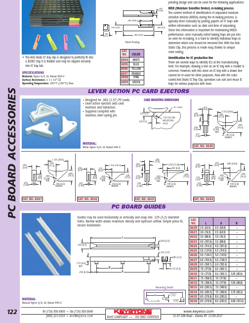
pending design and can be used for the following applications:MSD (Moisture Sensitive Device)re-baking process The current method of identification of unpacked moisture sensitive devices (MSDs)during the re-baking process,is typically done manually by pasting papers on IC trays with written information such as date and time of unpacking.Since this information is important for maintaining MSDs performance,once manually noted baking trays are put into an oven for re-baking,it is hard to identify individual trays to determine which one should be removed first.With the Anti-Static Clip,this process is made easy,thanks to unique color coding.Identification for IC production lineThere are several ways to identify ICs at the manufacturing level.For example,drawing a line on an IC tray with a marker is common.However,with this done an IC tray with a drawn line cannot be re-used for other purposes.Now with the color coded Anti-Static IC Tray Clip,operators can sort and reuse IC trays for various purposes with ease.CAT.NO.COLOR8894WHITE 8895BLUE 8896YELLOW 8897ORANGE 8898PINK 8899GREENCAT.NO.L A B 8620 2.5(63.5) 2.0(50.8)—8621 3.0(76.2) 2.5(63.5)—8622 3.5(88.9) 3.0(76.2)—8623 4.0(101.6) 3.5(88.9)—8624 4.5(114.3) 4.0(101.6)—8625 5.0(127.0) 4.5(114.3)—8626 5.5(139.7) 5.0(127.0)—8627 6.0(152.4) 5.5(139.7)—8628 6.5(165.1) 6.0(152.4)—86297.0(177.8) 6.5(165.1)—86307.0(177.8) 6.5(165.1) 3.25(82.6)86317.5(190.5)7.0(177.8)—86327.5(190.5)7.0(177.8) 3.50(88.9)86338.0(203.2)7.5(190.5)—86348.0(203.2)7.5(190.5) 3.75(95.3)86358.5(215.9)8.0(203.2)—86368.5(215.9)8.0(203.2)4.00(101.6)•Designed for .062(1.57)PC cards.•Level action ejectors aids cardinsertion and extraction.•Supplied complete with stainless steel spring pin.LEVER ACTION PC CARD EJECTORSCARD MOUNTING DIMENSIONSPC BOARD GUIDES.109[2.8]DIA.MOUNTING HOLE.250[6.4].250 [6.4]PC CARD.250 [6.4].140 [3.6]RADIUS.093[2.36]DIA.1.125 [28.6].450 [11.5].640 [16.3].075 [1.90].250[6.4].375[9.6]CAT.NO.8640CAT.NO.8644CAT.NO.8643CAT.NO.8641CAT.NO.8642.075 [1.90].390[9.9].640 [16.3].450 [11.5]1.125 [28.6].093[2.36]DIA..140 [3.6]RADIUS.250 [6.4].375[9.5] 1.100 [28.0].140[3.6]RADIUS.390[9.9].075 [1.90].250[6.4].093[2.36]DIA..520[13.2].600[15.3].093[2.36]DIA..140 [3.6]RADIUS1.250 [31.8].075 [1.90].250 [6.4].290[7.4].134[3.4].260 [6.6].250[6.4].140 [3.6]RADIUS.093[2.36]DIA..980 [24.9].375[9.5].640[16.3].390[9.9].125[3.2].075[1.90]Guides may be used horizontally or vertically and snap into .125(3.2)diameter holes.Narrow width allows maximum density and optimum airflow.Simple press-fit,secure installation.MATERIAL:Natural Nylon 6/6,UL Rated 94V-2B.125[3.2].250[6.4].132 [3.4].078 [2.0].245[6.2]LA.085[2.2].172[4.4]REF ..185[4.7].197[5.01].205[5.2].984[25.0].394[10.0].075[1.90]Mounting Detail.218 [5.6](2)PLS.120[3.1](2)PLSAB.125 [3.2] DIA .SPECIFICATIONSMaterial:Nylon 6/6,UL Rated 94V-0Surface Resistance:≤1x 10¹²ΩOperating Temperature:300°F (150°C)Max.MATERIAL:White Nylon 6/6,UL Rated 94V-2Tel (718)956-8900•Fax (718)956-9040(800)221-5510•kec@31-0720th Road –Astoria,NY 11105-2017RoHS COMPLIANT ~ISO 9001CERTIFIED®Patent Pending•The Anti-Static IC tray clip is designed to perfectly fit into a JEDEC tray.It is flexible and may be clipped securely into IC tray tab.P C B O A R D A C C E S S O R I E S122分销商库存信息:KEYSTONE-ELECTRONICS889688978898 8899。

EUROPEBasingstoke, UK +44 1256 812812AUSTRALASIAQueenstown, SA, Australia +61 8 8240 2244CANADAGuelph, Ontario (519) 822-2960St. Laurent, Quebec (514) 343-9010USACheektowaga, NY (716) 651-0086w w w .h a mm o n d mf g .c o m20©Flanged Lid Version - Polystyrene (1591 Series)ACCESSORIESOTHER KEY FEATURES• Electronic instrument enclosures, designed for mounting printed circuit boards.• Designed for applications where the enclosure needs to be easily wall or shelf mounted.• Perfect where extra enclosure security is required by restricting access to lid screws.• Integral card guides accept 1.5 mm (0.062”) P .C. cards.• Two piece lap joint construction provides protection against access of dust and splashing water.• Designed to meet IP54• Molded in economical black polystyrene.• Lid is secured with black self-tapping #4 x 0.5” Philips screws.Unit assembled with self-tappingscrews...Economical black polystyrene material...Lap joint construction...P .C. Board Card Adaptors Allows horizontal mounting of P.C.board(s). See “Accessories Section” for full details!1591Z6 - Package of 61591Z50 - Package of 501591Z100 - Package of 100Replacement Screws Self-tapping type, black oxide,#4 x 0.5”1591TS100BK- Package of 100P .C. board standoffs molded into lid...P .C. Board ScrewsSelf-tapping type, used for bosses in the 1591 lid for P .C. board installation. #4 x 1/4” (6.4 mm)1593ATS50 - Package of 501593ATS100 - Package of 100芯天下--/21w w w .h a m m o n d mf g .c o m©CANADAGuelph, Ontario (519) 822-2960St. Laurent, Quebec (514) 343-9010USACheektowaga, NY (716) 651-0086EUROPEBasingstoke, UK +44 1256 812812AUSTRALASIAQueenstown, SA, Australia +61 8 8240 2244Flanged Lid Version - Polystyrene (1591 Series)For detailed drawings, CAD files and color photos visitour website at:NOTES:- Assembled height = dimension “C” + 0.16” (4.0 mm)- Average wall thickness: 0.08” (2.0 mm)芯天下--/。
Features•Eight (8) Outputs Rated at 60V , -120mA •Open-Drain, Pull-Up Driver Configuration •6V to 60V Driver Supply Range •2.7V to 5.5V Logic Supply Range•3-Wire Serial Interface plus Chip Select •Captures Serial & Parallel Input Data •Outputs Can Be Paralleled •28-Lead QFN PackageApplications•White Goods •A TE•Industrial EquipmentDescriptionThe MX879 is an 8-channel, high voltage switch with 8-bit parallel or serial input control. The MX879 connects directly to a microprocessor through a standard 3-wire serial interface. The open-drain,pull-up output configuration can drive up to 60 volts at -120mA. Outputs can be paralleled for increased drive current up to a device total of 600mA source.The MX879 is designed to operate over a temperature range of -40°C to +85°C, and is available in a 28-lead QFN Package.Ordering InformationFunctional Block DiagramPartDescriptionMX879R QFN-28 (73/T ube)MX879RTRQFN-28 T ape & Reel (2500/Reel)1. Specifications . . . . . . . . . . . . . . . . . . . . . . . . . . . . . . . . . . . . . . . . . . . . . . . . . . . . . . . . . . . . . . . . . . . . . . . . . . . . . . . . . . . . . . . . . . . . . . 31.1 Package Pinout . . . . . . . . . . . . . . . . . . . . . . . . . . . . . . . . . . . . . . . . . . . . . . . . . . . . . . . . . . . . . . . . . . . . . . . . . . . . . . . . . . . . . . . . . 31.2 Pin Description. . . . . . . . . . . . . . . . . . . . . . . . . . . . . . . . . . . . . . . . . . . . . . . . . . . . . . . . . . . . . . . . . . . . . . . . . . . . . . . . . . . . . . . . . . 31.3 Absolute Maximum Ratings. . . . . . . . . . . . . . . . . . . . . . . . . . . . . . . . . . . . . . . . . . . . . . . . . . . . . . . . . . . . . . . . . . . . . . . . . . . . . . . . 41.4 DC Electrical Characteristics. . . . . . . . . . . . . . . . . . . . . . . . . . . . . . . . . . . . . . . . . . . . . . . . . . . . . . . . . . . . . . . . . . . . . . . . . . . . . . . 41.5 Dynamic Electrical Characteristics. . . . . . . . . . . . . . . . . . . . . . . . . . . . . . . . . . . . . . . . . . . . . . . . . . . . . . . . . . . . . . . . . . . . . . . . . . . 51.6 Serial Timing . . . . . . . . . . . . . . . . . . . . . . . . . . . . . . . . . . . . . . . . . . . . . . . . . . . . . . . . . . . . . . . . . . . . . . . . . . . . . . . . . . . . . . . . . . . 61.7 Parallel Timing. . . . . . . . . . . . . . . . . . . . . . . . . . . . . . . . . . . . . . . . . . . . . . . . . . . . . . . . . . . . . . . . . . . . . . . . . . . . . . . . . . . . . . . . . . 62. Functional Description . . . . . . . . . . . . . . . . . . . . . . . . . . . . . . . . . . . . . . . . . . . . . . . . . . . . . . . . . . . . . . . . . . . . . . . . . . . . . . . . . . . . . . . 73. Application Examples. . . . . . . . . . . . . . . . . . . . . . . . . . . . . . . . . . . . . . . . . . . . . . . . . . . . . . . . . . . . . . . . . . . . . . . . . . . . . . . . . . . . . . . . 83.1 Parallel In / Parallel Out Application. . . . . . . . . . . . . . . . . . . . . . . . . . . . . . . . . . . . . . . . . . . . . . . . . . . . . . . . . . . . . . . . . . . . . . . . . . 83.2 Serial Cascade Application . . . . . . . . . . . . . . . . . . . . . . . . . . . . . . . . . . . . . . . . . . . . . . . . . . . . . . . . . . . . . . . . . . . . . . . . . . . . . . . . 83.3 Control System Application . . . . . . . . . . . . . . . . . . . . . . . . . . . . . . . . . . . . . . . . . . . . . . . . . . . . . . . . . . . . . . . . . . . . . . . . . . . . . . . . 94. Manufacturing Information. . . . . . . . . . . . . . . . . . . . . . . . . . . . . . . . . . . . . . . . . . . . . . . . . . . . . . . . . . . . . . . . . . . . . . . . . . . . . . . . . . . 104.1 Moisture Sensitivity . . . . . . . . . . . . . . . . . . . . . . . . . . . . . . . . . . . . . . . . . . . . . . . . . . . . . . . . . . . . . . . . . . . . . . . . . . . . . . . . . . . . . 104.2 ESD Sensitivity . . . . . . . . . . . . . . . . . . . . . . . . . . . . . . . . . . . . . . . . . . . . . . . . . . . . . . . . . . . . . . . . . . . . . . . . . . . . . . . . . . . . . . . . 104.3 Reflow Profile. . . . . . . . . . . . . . . . . . . . . . . . . . . . . . . . . . . . . . . . . . . . . . . . . . . . . . . . . . . . . . . . . . . . . . . . . . . . . . . . . . . . . . . . . . 104.4 Mechanical Dimensions. . . . . . . . . . . . . . . . . . . . . . . . . . . . . . . . . . . . . . . . . . . . . . . . . . . . . . . . . . . . . . . . . . . . . . . . . . . . . . . . . . 111Specifications1.1 Package Pinout1.2 Pin DescriptionPin#Name Description1OUT7Parallel Output 2N/C No Connection 3GND Ground4V PWR High Voltage Supply (6V to 60V)5N/C No Connection6V CC Logic Supply (2.7V to 5.5V)7SDO Serial Data Output 8IN7Parallel Input 9IN6Parallel Input 10IN5Parallel Input 11IN4Parallel Input 12IN3Parallel Input 13IN2Parallel Input 14IN1Parallel Input 15IN0Parallel Input 16SCK Serial Clock17V PWR High Voltage Supply (6V to 60V)18SDI Serial Data Input 19CS*Chip Select (Active Low)20OE Output Enable 21GND Ground 22OUT0Parallel Output 23OUT1Parallel Output 24OUT2Parallel Output 25OUT3Parallel Output 26OUT4Parallel Output 27OUT5Parallel Output 28OUT6Parallel Output1.3 Absolute Maximum RatingsVoltages with respect to GND=0V .Absolute maximum electrical ratings are at 25°CAbsolute Maximum Ratings are stress ratings. Stresses in excess of these ratings can cause permanent damage to the device. Functional operation of the device at these or any other conditions beyond those indicated in the operational sections of this data sheet is not implied.Exposure of the device to the absolute maximum ratings for an extended period may degrade the device and affect its reliability.ESD Warning: ESD (electrostatic discharge) sensitive device. Although the MX879 features proprietary ESD protectioncircuitry, permanent damage may be sustained if subjected to high energy electrostatic discharges. Proper ESD precautions are recommended to avoid performance degradation or loss of functionality.1.4 DC Electrical CharacteristicsV CC =5V , V PWR =42V , T A =25°C, unless otherwise specified.Notes:T o avoid unwanted output during VPWR application and system initialization, keep OE at a logic low until CS* has completed one cycle.Thermal Resistance is measured in still air with the device soldered to a 6 square inch board without a ground plane. Applications may require derating of the specified maximum currents to avoid exceeding the maximum operation junction temperature.ParameterSymbolMinMaxUnitsVPWR Supply Voltage V PWR -60V Logic Supply Voltage V CC -6V Input Pin Voltage VIN -6V Continuous Output Current OUT0 - OUT7I OUTn --150mA Operating Junction T emperature T J -150°C Thermal Resistance (Junction to Ambient)R θJA 110 T ypical °C/W Operating T emperature T A -4085°C Storage T emperatureT STG-55150°CParameterConditionsMinimumTypicalMaximumUnitsLogic Supply Voltage - 2.7- 5.5V Logic Supply Current f SCK =5MHz -50-μA Quiescent Logic Supply Current f SCK =0--1μA V PWR Voltage -6-60V V PWR Current T otal of all Outputs --600mA Quiescent V PWR Current V PWR =42V , No Load -0.75-mA High Level Input Voltage IN0-IN7, SCK, SDI, OE, CS*V CC -0.5--V Low Level Input Voltage ---0.5V Input Leakage Current ---1μA SDO T ri-State Leakage Current CS*=Logic High --1μA OUT0-OUT7 Current Any One Output, Source---120mA OUT0-OUT7 ON Resistance V PWR =42V -7-ΩOUT0-OUT7 T ri-State Leakage CurrentOE=Logic Low--1μA1.5 Dynamic Electrical CharacteristicsV CC=5V, V PWR=42V, T A=25°C, unless otherwise specified.Parameter Conditions Symbol Minimum Typical Maximum Units SCK Period--100-DC ns SCK High Time--40--ns SCK Low Time--40--ns CS* High Time-tCSwh50--ns CS* Falling to SCK Rising Setup Time tCSs150--ns CS* Low Time SCK Low (Parallel Input Mode)tCSwl150--ns INx to CS Falling (SETUP TIME)-tINs15--ns INx to CS Falling (HOLD TIME)-tINh30--ns SDI to SCK Rising (SETUP TIME)-tSDIs20--ns SDI to SCK Rising (HOLD TIME)-tSDIh25--nsSCK Falling to to SDO Data Valid-tSDO-10-ns CS* Rising to SDO High Z-tSDOz-12-ns CS* Rising to OUTx Rising T o 50%, C(OUTx)=1000pF tOUT r-680-ns OUTx Rise Time From 10% to 90%, C(OUTx)=1000pF--110-ns OE Rising to OUTx Rising T o 90%--580-ns OE Rising to OUTx Falling T o 90%--390-nsOE Falling to OUTx High Z T o 10%, OUTx High--130-nsT o 10%, OUTx Low--90-ns1.6 Serial Timing1.7 Parallel Timing2Functional DescriptionThe MX879 is an 8-channel high-voltage driver with 8-bit input control. The MX879 interfaces to a microprocessor through a standard 3-wire serial interface and an active-low chip select, or can be used in a parallel-in, parallel-out configuration.Parallel data is transferred to the I/O register of the MX879 through the parallel input pins, IN0 throughIN7, on the falling edge of the chip select pin, CS*. When CS* is in a logic-low state, serial data can be transferred to the I/O register through the serial input pin, SDI, and from the I/O register through the serial output pin, SDO. Parallel or serial input data is transferred from the I/O register to the latch and high voltage output drivers, OUT0 through OUT7, on the positive edge of CS*. This data remains latched until the next positive edge of CS*.The 8-bit I/O shift register is clocked by the serial clock pin, SCK. Serial data presented at the SDI pin is transferred to the shift register on the positive edge of SCK. Data shifts out of the register through the SDO pin on the negative edge of SCK. SDI and SCK are ignored, and SDO transitions to a high impedance condition when CS* is at a logic high state.Serial data is received by the MX879 through the SDI pin. This data is accepted on the rising edge of SCK. A specific output is programmed to a logic-high state if SDI is at a logic-high state during the rising edge of SCK. Conversely, a specific output is programmed to a logic-low state if SDI is at a logic-low state during the rising edge of SCK. Outputs transition to their programmed states on the positive edge of CS* if the output enable pin, OE, is in a logic-high state.The MSB input data (IN7) is presented at the serial output pin, SDO, on the falling edge of CS*. Input data from IN6 through IN0 is sequentially presented at SDO on negative SCK transitions if CS* remains in a logic-low state. If CS* is at a logic-low state beyond 8 cycles of SCK, SDI data that has propagated through the I/O register will then be presented at SDO. The SDO pin transitions to a high-impedance state when CS* is in a logic-high state, thus allowing multiple serial peripherals to share the microprocessor data pin.Figure 1. Serial Data Transfer ExampleDevices may be serially cascaded by connecting SDO to SDI of the next device. Pins SCK and CS* are common to all devices in serial cascade. Forn-cascaded devices the CS* should remain low for 8n cycles of SCK.An output enable pin, OE, enables the driver outputs OUT0 through OUT7 when logic-high. A logic-low level on OE forces the OUT0 through OUT7 outputs to a high-impedance state.The MX879 can also operate as a parallel-in, parallel-out level shifter and driver. SCK must remain at a logic-low state when operating in this mode. Parallel input data presented to IN0 through IN7 is captured on the falling edge of CS*. This data is transferred to OUT0 through OUT7 on the rising edge of CS*, and remains latched until the next rising edge of CS*.3Application Examples3.1 Parallel In / Parallel Out Application3.2 Serial Cascade Application3.3 Control System Application4Manufacturing Information4.1 Moisture SensitivityAll plastic encapsulated semiconductor packages are susceptible to moisture ingression. Clare classified all of its plastic encapsulated devices for moisture sensitivity according to the latest version of the joint industry standard, IPC/JEDEC J-STD-020, in force at the time of product evaluation. We test all of our products to the maximum conditions set forth in the standard, and guarantee proper operation of ourdevices when handled according to the limitations and information in that standard as well as to any limitations set forth in the information or standards referenced below.Failure to adhere to the warnings or limitations as established by the listed specifications could result in reduced product performance, reduction of operable life, and/or reduction of overall reliability.This product carries a Moisture Sensitivity Level (MSL) rating as shown below, and should be handled according to the requirements of the latest version of the joint industry standard IPC/JEDEC J-STD-033.4.2 ESD SensitivityThis product is ESD Sensitive , and should be handled according to the industry standard JESD-625.4.3 Reflow ProfileThis product has a maximum body temperature and time rating as shown below. All other guidelines of J-STD-020 must be observed.Device Moisture Sensitivity Level (MSL) RatingMX879RMSL 3Device Maximum Temperature x TimeMX879R260°C for 30 seconds分销商库存信息:IXYSMX879RTR MX879R。