Xilinx EDK官方试验4mb
- 格式:pdf
- 大小:317.93 KB
- 文档页数:13

Chapter1 Package InformationPackage OverviewIntroduction to Xilinx PackagingElectronic packages are interconnectable housings for semiconductor devices. The majorfunctions of the electronic packages are to provide electrical interconnections between theIC and the board and to efficiently remove heat generated by the device.Feature sizes are constantly shrinking, resulting in increased number of transistors beingpacked into the device. Today's submicron technology is also enabling large-scalefunctional integration and system-on-a-chip solutions. In order to keep pace with thesenew advancements in silicon technologies, semiconductor packages have also evolved toprovide improved device functionality and performance.Feature size at the device level is driving package feature sizes down to the design rules ofthe early transistors. To meet these demands, electronic packages must be flexible toaddress high pin counts, reduced pitch and form factor requirements. At the same time,packages must be reliable and cost effective.Packaging T echnology at XilinxXilinx provides a wide range of leaded and array packaging solutions for our advancedsilicon products. Xilinx® advanced packaging solutions include overmolded plastic ballgrid arrays (PBGA), small form factor Chip Scale Packages, “Cavity-Down” BGAs,flip-chip BGAs, flip-chip ceramic column grid arrays (CCGA), as well as the newer leadframe packages such as Quad Flat No-Lead (QFN) packages to meet various pin countsand density requirements. Packages from Xilinx are designed, optimized, andcharacterized to support the long-term mechanical reliability requirements as well as tosupport the cutting-edge electrical and thermal performance requirements for our high-speed advanced FPGA products.Pb-free Packaging Solutions from XilinxXilinx also develops packaging solutions that are safer for the environment. Today,standard packages from Xilinx do not contain substances that are identified as harmful tothe environment including cadmium, hexavalent chromium, mercury, PBB, and PBDE. Pb-free solutions take that one step further and also do not contain lead (Pb). This makes Pb-free solutions from Xilinx RoHS (Reduction of Hazardous Substances) compliant. Pb-freepackages from Xilinx are also JEDEC J-STD-020 compliant, meaning that the packages aremade to be more robust so they are capable of withstanding higher reflow temperatures.Xilinx is now ready to support the industry requirements for Pb-free packaging solutions.Chapter 1:Package InformationPackage SamplesXilinx offers two types of non-product-specific package samples that can help developcustom processes and perform board-level tests. These samples can be ordered withordering codes as detailed below.Mechanical Samples XCMECH-XXXXX (where XXXXX is the package code of interest)This part type is used for mechanical evaluations, process setup, etc. Most packages arebased on the JEDEC outline, and these parts are at times referred to as "dummy" parts sincemechanical samples do not contain a die.Example:To order a FG676 package as a mechanical sample (without the die), the part numberwould be XCMECH-FG676.质量等级领域:宇航级IC、特军级IC、超军级IC、普军级IC、禁运IC、工业级IC,军级二三极管,功率管等;应用领域:航空航天、船舶、汽车电子、军用计算机、铁路、医疗电子、通信网络、电力工业以及大型工业设备祝您:工作顺利,生活愉快!以赛灵思半导体(深圳)有限公司提供的参数为例,以下为XC7VX415T-2FFG1158C的详细参数,仅供参考Specifications and DefinitionsDaisy Chain Samples XCDAISY-XXXXX (where XXXXX is the package code of interest)Use this part type to perform board-based evaluations (such as vibrations and temperaturecycles) to see how well the solder balls withstand these mechanical conditions. For Xilinxdaisy chain parts (XCDAISY-XXXXX), a specific ball assignment chain is available. If youdo not have a board already made, you can use our default chain. You can purchase theseparts from Xilinx through standard sales outlets. Xilinx does not support unique chainsbecause these parts do not have the volume to justify the development effort.Example:To order a FG676 package in a daisy-chained configuration, the part number would beXCDAISY-FG676.Specifications and DefinitionsInches vs. MillimetersThe JEDEC standards for PLCC, CQFP, and PGA packages define package dimensions ininches. The lead spacing is specified as 25mils, 50mils, or 100mils (0.025in., 0.050in. or0.100in.).The JEDEC standards for PQFP, HQFP, TQFP, VQFP, CSP, and BGA packages definepackage dimensions in millimeters. The lead frame packages have lead spacings of0.5mm, 0.65mm, or 0.8mm. The CSP and BGA packages have ball pitches of 0.5mm,0.8mm, 1.00mm, or 1.27mm.Because of the potential for measurement discrepancies, this Data Book providesmeasurements in the controlling standard only, either inches or millimeters.Pressure Handling CapacityFor mounted BGA packages, including flip chips, a direct compressive (non-varying) forceapplied normally to the lid or top of package with a tool head that coincides with the lid (oris slightly bigger) will not induce mechanical damage to the device including externalballs, provided the force is not over 5.0 grams per external ball, and the device and boardare supported to prevent any flexing or bowing.These components are tested in sockets with loads in the 5 to 10 gm/ball range for shortdurations. Analysis using a 10g/ball (e.g., 10 kg for FF1148) showed little impact on short-term but some creep over time. 20 gm/ball and 45 gm/ball loads at 85°C over a six weekperiod has shown the beginning of bridging of some outer balls; these were static loadtests. The component can survive forces greater than the 5 gm limit while in short-termsituations. However, sustained higher loads should be avoided (particularly if they areoverlaid with thermal or power cycle loads). Within the recommended limits, circuit boardneeds to be properly supported to prevent any flexing resulting from force application.Any flexing or bowing resulting from such a force can likely damage the package-to-boardconnections. Besides the damage that can occur from bending, the only major concern islong-term creep and bulging of the solder balls in compression to cause bridging. For thelife of a part, staying below the recommended limit will ensure against that remotepossibility.Chapter 1:Package InformationClockwise or CounterclockwiseThe orientation of the die in the package and the orientation of the package on the PCboard affect the PC board layout. PLCC and PQFP packages specify pins in acounterclockwise direction, when viewed from the top of the package (the surface with theXilinx logo). PLCCs have pin 1 in the center of the beveled edge while all other packageshave pin 1 in one corner, with one exception: The 100-pin and 165-pin CQFPs (CB100 andCB164) for the XC3000 devices have pin 1 in the center of one edge.CQFP packages specify pins in a clockwise direction, when viewed from the top of thepackage. The user can make the pins run counterclockwise by forming the leads such thatthe logo mounts against the PC board. However, heat flow to the surrounding air isimpaired if the logo is mounted down.Cavity-Up or Cavity-DownMost Xilinx devices attach the die against the inside bottom of the package (the side thatdoes not carry the Xilinx logo). Called “Cavity-Up,” this has been the standard ICassembly method for over 25 years. This method does not provide the best thermalcharacteristics. Pin Grid Arrays (greater than 130 pins), copper based BGA packages, andCeramic Quad Flat Packs are assembled “Cavity-Down,” with the die attached to theinside top of the package, for optimal heat transfer to the ambient air. More information on“Cavity-Up” packages and “Cavity-Down” packages can be found in the “PackageTechnology Descriptions” section.For most packages this information does not affect how the package is used because theuser has no choice in how the package is mounted on a board. For Ceramic Quad Flat Pack(CQFP) packages however, the leads can be formed to either side. Therefore, for best heattransfer to the surrounding air, CQFP packages should be mounted with the logo up,facing away from the PC board.Part MarkingOrdering InformationAn example of an ordering code for a Xilinx FPGA is XC4VLX60-10FFG668CS2. Theordering code stands for:XC4VLX – Family (Virtex®-4 LX)60 – Number of system gates or logic cells (60,000 logic cells)-10 – Speed grade (-10 speed)FFG – Package type (Pb-free flip-chip BGA)668 – number of pins (668 pins)C – Temperature grade (Commercial)S2 – Step 2Part MarkingChapter 1:Package Information。

试验6系统验证及调试:介绍这个试验通过XMD和ChipScope 对系统进行可观测的软件和硬件调试。
目标完成试验后,我们希望达到以下目标:•向系统中加入ChipScope片内逻辑分析仪•系统调试打开工程Step 1在D:\Lab\下创建lab6mb文件夹。
可以根据上面的实验建立工程,也可直接把lab6mb的内容直接拷贝至此目录。
编译器优化选项设置Step 2这个部分测试编译器优化水平的不同性能。
在这之前,我们要移除定时器中断服务程序用一个延时循环来代替它。
n使用Project → Software Platform Settings …打开软件平台设置GUIo点击Processor, Driver Parameters and Interrupt Handlers栏p删除Current Value的值timer_int_handler。
使其为空。
点击<OK>q从D:\Lab\lab_sources\lab6_sources路径复制system_delay.c到当前工程D:\Lab\labmb6\coder从工程MyProj移除system_timer.c并加入新的文件system_delay.cs双击MyProj标题选择Optimization Tab如图所示,设置编译器优先等级到No Optimization,点击<OK>。
图 6-1. 编译选项设置w选择Download那么这些源文件将重新编译并下载到板上去。
LED将连续0.1秒显示计数器。
w设置编译器优化等级,并再次下载到工程当中去。
注意显示速度取决于编译器的优化等级片内逻辑分析仪Step 3点击Project → Add/Edit Cores … (dialog),加入ChipScope 片内逻辑分析仪的。
配制以下端口。
如图6-2所示。
sys_clk_smb_halt (MicroBlaze)dbg_stop (MicroBlaze)图6-2 芯片域内核连接n 点击Project → Add Cores (dialog)o 在Peripherals 栏 加入chipscope_icon 与chipscope_opb_iba 参数p 在Bus connection 栏,连接chipscope_opb_iba 作为一个BA (总线分析器)器件到OPB 总线。

第0篇Xilinx FPGA开发环境的配置一、配置Modelsim ISE的Xilinx的仿真库1、编译仿真库:A、先将Modelsim安装目录C=Modeltech_6.2b下面的modelsim.ini改成存档格式(取消只读模式);B、在DOS环境中,进入Xilinx的根目录,然后依次进入bin,nt目录;C、运行compxlib -s mti_se -f all -l all -oC:Modeltech_6.2bxilinx_libs。
注意:需要根据你安装的modelsim目录更改C:Modeltech_6.2b 然后就Ok了,就可以的ISE中启动Modelsim进行所有的仿真了。
2、如何在Xilinx ISE中使用Modelsim ISE,Synplify进行综合和仿真:A、打开Xilinx ISE,新建一个Project;①、在菜单File中选择“New Project”,弹出如下的对话框:②、输入Project名称,并选择好Project保存的路径,然后下一步:字串3按照上边的参数进行设置(针对于Spatan 3E的开发板),然后单击下一步,进入到后面的界面:③、单击“New Source”按钮,并按照下面的设置来操作:④、参照下面的参数,进行设置,然后一直选择默认选项,一直到完成。
最后生成的项目界面如下图所示:B、输入代码,然后用Synplify综合:①、参考代码:entity Count iSPort(CLK :in STD_LOGIC;RESET :in STD_LOGIC;LOAD :in STD_LOGIC;DATA IN:in STD_LOGIC_VECTOR(3 downto 0);字串9Qout :out STD_LOGIC_VECTOR(3 downto 0));end Count;architecture Behavioral of Count issignal tmpCount:STD_LOGIC_VECTOR(3 downto 0);beginprocess(CLK,RESET,LOAD)beginif RESET='1' thentmpCount<="0000";elseif LOAD='1' thentmpCount<=DATA_IN;elsif CLK'event and CLK='1' thentmpCount<=tmpCount+1;end if;end if;end process; 字串6Qout<=tmpCount:end Behavioral;②、双击Processes窗口里面的“Synthesize-Synplify”进行综合③、在“Transcript”窗口中的可以看到综合的信息。
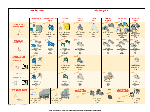
ABB EntrelecSommaireBU0402061SNC 160 003 C0205SummarySelection guide ....................................................................................page 1Screw clamp ........................................................................................page 2Feed through and ground terminal blocks .......................................................page 2 - 5 to 10Single pole, multiclamp terminal blocks..........................................................................page 4Feed through terminal blocks - Double-deck................................................................page 11Feed through terminal blocks - Triple-deck...................................................................page 12Three level sensor, terminal blocks without ground connection...................................page 13Three level sensor, terminal blocks with ground connection ........................................page 14Terminal blocks for distribution boxes, double deck + protection .......................page 15 - 16Interruptible terminal blocks for neutral circuit......................................................page 17 - 18Distribution : phase, ground terminal blocks .......................................................page 19 to 21Single pole or four pole distribution blocks..........................................................page 22 to 24Heavy duty switch terminal blocks with blade......................................................page 25 - 26Heavy duty switch terminal blocks with push-turn knob..............................................page 26Heavy duty switch terminal blocks with contact control pull lever...............................page 29Heavy duty switch terminal blocks with blade - Double-deck .....................................page 27Fuse holder terminal blocks for 5x20 mm (.197x.787 in.) and 5x25 mm (.197x.984 in.)or 6.35x25.4 mm (1/4x1 in.) and 6.35x32 mm (1/4x11/4 in.) fuse s.........................................page 28 - 29Fuse holder terminal blocks for 5x20 mm (.197x.787 in.) and 5x25 mm (.197x.984 in.) fuses -Double-dec k.....................................................................................................................page 27Terminal blocks for test circuits with sliding bridge ......................................................page 30Terminal blocks for metering circuits.............................................................................page 31ESSAILEC terminal blocks.............................................................................................page 32Safety connection terminal blocks ................................................................................page 33Miniblocks for EN 50045 (DIN 46277/2) rail ..........................................................page 34 - 35Spring clamp ......................................................................................page 36Angled terminal blocks - Feed through and ground .....................................................page 36Feed through and ground terminal blocks ...........................................................page 37 to 41Feed through terminal blocks - Double deck ................................................................page 42Terminal blocks for sensors / actuators ........................................................................page 42Terminal blocks for distribution boxes...........................................................................page 43Switch terminal blocks for neutral conductor........................................................page 44 - 45Heavy duty switch terminal blocks with blade..............................................................page 46Fuse holder terminal blocks for 5x20 mm (.197x.787 in.) and 5x25 mm (.197x.984 in.) fuse s....page 47Miniblocks Spring clamp ......................................................................................page 48 to 52ADO - Screw clamp ...........................................................................page 53Feed through and ground terminal blocks ...........................................................page 53 to 56Feed through and ground terminal blocks - Double-deck............................................page 57Heavy duty switch terminal blocks with blade..............................................................page 58Fuse holder terminal blocks for 5x20 mm (.197x.787 in.) and 5x25 mm (.197x.984 in.) fuse s ......page 59 - 60Miniblocks ADO - Screw clamp............................................................................page 61 to 65ADO - ADO .........................................................................................page 66Feed through and ground terminal blocks ...........................................................page 66 to 69Feed through and ground terminal blocks - Double-deck............................................page 70Terminal blocks for sensors / actuators ........................................................................page 71Heavy duty switch terminal blocks with blade..............................................................page 72Fuse holder terminal blocks for 5x20 mm (.197x.787 in.) and 5x25 mm (.197x.984 in.) fuse s ......page 73 - 74Miniblocks ADO - ADO .........................................................................................page 75 to 79Accessories ADO ...........................................................................................................page 80Power terminal blocks .............................................................page 81 to 84Quick-connect terminal blocks .................................................page 85 - 86Terminal blocks for railway applications ................................page 87 to 97Pluggable terminal blocks .....................................................page 98 to 100Accessories......................................................................................page 101Marking..................................................................................page 102 to 104GrossAutomation(877)268-3700··*************************PR30PR3.Z2PR3.G2PR5PR4PR1.Z2Rated wire size :Rated wire size :Rated wire size :Rated wire size :Mounting railsShield terminals forcollector barMarking tableHorizontal Rated wire size :0.5 to 16 mm² (22 to 8 AWG)Rated wire size :Rated wire size :Rated wire size :P a g e t o 29e30 t o 32ag e e3P a ge 8 t o 60a g e6t o 6574P a ge 7 t o 79P a ge 9P a g P a gGrossAutomation(877)268-3700··*************************2ABB Entrelecd010830402051SNC 160 003 C0205MA 2,5/5 - 2.5 mm² blocks - 5 mm .200" spacingAccessoriesGrossAutomation(877)268-3700··*************************3ABB Entrelec D010740402051SNC 160 003 C0205M 4/6 - 4 mm² blocks - 6 mm .238" spacingAccessoriesGrossAutomation(877)268-3700··*************************4ABB EntrelecD011030402051SNC 160 003 C0205M 4/6.3A - 4 mm² blocks - 6 mm .238" spacingM 4/6.4A - 4 mm² blocks - 6 mm .238" spacingGrossAutomation(877)268-3700··*************************5ABB Entrelec D010840402051SNC 160 003 C0205M 6/8 - 6 mm² blocks - 8 mm .315" spacingAccessoriesGrossAutomation(877)268-3700··*************************6ABB EntrelecD010850402051SNC 160 003 C0205M 10/10 - 10 mm² blocks - 10 mm .394" spacingAccessoriesGrossAutomation(877)268-3700··*************************7ABB Entrelec D010860402051SNC 160 003 C0205M 16/12 - 16 mm² blocks - 12 mm .473" spacingAccessoriesGrossAutomation(877)268-3700··*************************8ABB EntrelecD010870402051SNC 160 003 C0205M 35/16 - 35 mm² blocks - 16 mm .630" spacingGrossAutomation(877)268-3700··*************************M 95/26 - 95 mm² blocks - 26 mm 1.02" spacingM 70/22.P - 70 mm² ground block with rail contact - 22 mm .630" spacingSelection35 mm / 1.37"12 mm / 0.47"14-30 Nm / 124-260 Ib.in 1.2-1.4 Nm / 10.6-12.3 Ib.in1000600600415400400577070240 mm 2500 MCM 500 MCM 10 mm 2 6 AWG 6 AWG IEC UL CSANFC DIN0.5 - 160.5 - 100 AWG-600 MCM 2 AWG-500 MCM 50 - 30035 - 24018-6 AWGD 150/31.D10 - 150 mm² blocks - 31 mm 1.22" spacingCharacteristicsD 240/36.D10 - 240 mm² blocks - 36 mm 1.41" spacingSelectionWire size main circuit mm² / AWG VoltageV Current main circuit A Current outputARated wire size main circuit mm² / AWG Rated wire size outputmm² / AWG Wire stripping length main circuit mm / inches Wire stripping length output mm / inches Recommended torque main circuit Nm / Ib.in Recommended torque outputNm / Ib.inSolid Stranded Solid Stranded Wire size output mm² / AWG9.5 mm / .37"0.5-0.8 Nm / 4.4-7.1 Ib.in5003003003220204 mm 212 AWG12 AWG0.2 - 422-12 AWG 22-12 AWG 0.22 - 4IEC ULCSANFC DINCharacteristicsWire size mm² / AWGSolid Stranded D 4/6.T3 - 4 mm² blocks - 6 mm .238" spacingSelectionVoltage V CurrentARated wire sizemm² / AWG Wire stripping length mm / inches Recommended torqueNm / Ib.inM 4/6.T3.P - 4 mm² block - 6 mm .238" spacingD 2,5/6.D - 2.5 mm² blocks - 6 mm .238" spacingD 2,5/6.DL - 2.5 mm² blocks - 6 mm .238" spacingD 2,5/6.DPA1 - 2.5 mm² blocks - 6 mm .238" spacingD 2,5/6.DPAL1 - 2.5 mm² blocks - 6 mm .238" spacingD 4/6... - 4 mm² blocks - 6 mm .238" spacingD 4/6.LNTP - 4 mm² closed blocks - 17.8 mm .700" spacingMA 2,5/5.NT- 2.5 mm² block - 5 mm .200" spacingAccessories**SFB2 : 16 to 35 mm² 6 to 2 AWG H= 3 mm/.12"M 10/10.NT- 10 mm² block - 10 mm .394" spacingAccessories(1) Except for M 35/16 NT (closed block)*SFB1 : 0.5 to 35 mm² 18 to 2 AWG H= 7 mm/.28"**SFB2 : 16 to 35 mm² 6 to 2 AWG H= 3 mm/.12"MB 4/6... - 4 mm² blocks - 6 mm .238" spacingMB 6/8... - 6 mm² blocks - 8 mm .315" spacingMB 10/10... - 10 mm² blocks - 10 mm .394" spacingBRU 125 A - 35 mm² block - 27 mm 1.063" spacingBRU 160 A - 70 mm² block - 35.2 mm 1.388" spacingBRU 250 A - 120 mm² blocks - 44.5 mm 1.752" spacingBRU 400 A - 185 mm² block - 44.5 mm 1.752" spacingAccessoriesAccessoriesBRT 80 A - 16 mm² block - 48 mm 1.89" spacingBRT 125 A - 35 mm² block - 48 mm 1.89" spacingBRT 160 A - 50 mm² block - 50 mm 1.97" spacing9.5 mm / .37"0.5-0.6 Nm / 4.4-5.3 Ib.in4003003002010104 mm 210 AWG 12 AWG 0.5 - 422-10 AWG20-12 AWG0.5 - 2.5IEC ULCSANFC DINMA 2,5/5.SNB - 2.5 mm² blocks - 5 mm .200" spacingCharacteristicsM 4/6.SNB - 4 mm² blocks - 6 mm .238" spacingSelectionWire size mm² / AWGVoltage V CurrentARated wire sizemm² / AWG Wire stripping length mm / inches Recommended torqueNm / Ib.inSolid StrandedM 6/8.SNB - 6 mm² blocks - 8 mm .315" spacing - blade switchingSelectionAccessoriesM 4/8.D2.SF - for fuses 5x20 mm .197x.787 in. and 5x25 mm .197x.984 in. -4 mm² blocks - 8 mm .315" spacingM 4/6.D2.SNBT - 4 mm² blocks - 6 mm .238" spacing - blade switchM 4/8.SF- 4 mm² blocks - 8 mm .315" spacingM 4/8.SFL - 4 mm² blocks - 8 mm .315" spacing12 mm / .472"1.2-1.4 Nm / 10.6-12.3 Ib.in800(1)60060016252510 mm 210 AWG8 AWG0.5 - 1622-10 AWG 22-8 AWG 0.5 - 10IEC ULCSANFC DINCBD2SML 10/13.SF - for fuses 6.35x25.4 mm 1/4x1 in. and 6.35x32 mm 1/4x11/4 in. -10 mm² blocks - 13 mm .512" spacingSelectionAccessoriesCharacteristicsWire size mm² / AWGVoltage V CurrentARated wire sizemm² / AWG Wire stripping length mm / inches Recommended torqueNm / Ib.inSolid Stranded (1) Insulation voltage of terminal block - operating voltage : according to fuse.M 4/6.D2.2S2... - 4 mm² blocks - 6 mm .238" spacing11 mm / .43"0.8-1 Nm / 7.1-8.9 Ib.in50060030306 mm 28 AWG0.5 - 1022-8 AWG0.5 - 6IECULCSANFC DINM 6/8.ST... - 6 mm² blocks - 8 mm .315" spacingCharacteristicsWire size mm² / AWGVoltage V CurrentARated wire sizemm² / AWG Wire stripping length mm / inches Recommended torqueNm / Ib.inSolid Stranded M 6/8.STA - 6 mm² blocks - 8 mm .315" spacing(3)Only for M 6/8.STAM 4/6.ST- 4 mm² blocks - 6 mm .236" spacingBNT...PC...(2) Only for M10/10.ST-SnThe PREM IUM solution for testing the secondary circuits of current or voltage transformers.ESSAILEC, approved by the major electricity utilities, remains the premium choice for the energy market.Implemented in the transformers secondary circuits, ESSAILEC thanks to its intelligent “make before break” design eases and secures any intervention. Cutting the energy supply is avoided with zero risk for the operator.The plug and socket connection cuts cost installation as well as in-situ wiring errors. ESSAILEC is ideal for the wiring of sub-assemblies in the secondary circuits.ESSAILEC terminal blocksProtection relays,Protection relays,Testing :The ESSAILEC socket supplies energy to the protection or counting devices. The insertion of the test plug, which is connected to the measurement equipment, allows the testing of the devices, without perturbing the circuit.ESSAILEC blocks are well adapted to current or voltage measurement :-Current sockets with make before break contacts and pre-wired test plug for current measures-Voltage sockets with open contacts and pre-wired test plug for voltage measures-Up to 4 ammeters or 4 voltmeters connected to the test plugDistributing :The ESSAILEC plug is continuously mounted on the socket to supply current or voltage to secondary circuits sub assemblies.ESSAILEC blocks extreme versatility allow :-Safe current distribution with current socket with mobile contacts since the secondary circuit is not cut when plug is removed-Voltage or polarity distribution with dedicated voltage or polarity socket with closed contactESSAILEC is designed to offer :Great flexibility :-Connection multi contacts « plug and play »-Panel, rail, rack fixed mounting or stand-alone connector -Two wiring technologies, up to 10 mm²Extreme reliability :-Non symmetric blocks -Coding accessories -IP20 design -Locking system -Sealed coverR S T NFor technical characteristics and complete part numbers list, please ask for the ESSAILEC catalog10005006003225254 mm 21.65 mm²12 AWG 13 mm / .51"IECB.SCSANFC DINTS 50-180.5 - 0.8 Nm /4.4 - 7.1 Ib.in0.2 - 422-12 AWG0.22 - 40.5 - 1.50.28 - 1.6580050060041252562.512 AWG 13 mm / .51"0.8 - 1 Nm / 7.1 - 8.9 Ib.inIECB.S CSANFC DINTS 50-180.5 - 1020-12 AWG0.5 - 60.28 - 2.590050060046406510 mm 26 mm² 6 AWG 14 mm / .55"IECB.S UL/CSANFC DINTS 50-181.2 - 1.4 Nm / 10.6 - 12.3 Ib.in0.5 - 1620 - 6 AWG0.5 - 100.28 - 6M 4/6.RS - 4 mm² blocks - 6 mm .238" spacingCharacteristicsWire size mm² / AWGVoltage V CurrentARated wire sizemm² / AWG Wire stripping lengthmm / inches Recommended torque (screw)Nm / Ib.inSolid wire Stranded wire Solid wire Stranded wire Screw clampLugsM 6/8.RS - 6 mm² blocks - 8 mm .315" spacingCharacteristicsWire size mm² / AWGVoltage V CurrentARated wire sizemm² / AWG Wire stripping lengthmm / inches Recommended torque (screw)Nm / Ib.inSolid wire Stranded wire Solid wire Stranded wire Screw clampLugspending M 10/10.RS - 10 mm² blocks - 10 mm .394" spacingCharacteristicsWire size mm² / AWGVoltage V CurrentARated wire sizemm² / AWG Wire stripping lengthmm / inches Recommended torque (screw)Nm / Ib.inSolid wire Stranded wire Solid wire Stranded wire Screw clampLugspending SelectionAccessories(1) Only for block M 4/6.RS (4) For blocks M 4/6.RS and M 6/8.RS(2) Only for block M 6/8.RS(3) Only for block M 10/10.RSDR 1,5/4 - 1.5 mm² blocks - 4 mm .157" spacingDR 1,5/5... - 1.5 mm² blocks - 5 mm .200" spacing。

今天在网上的高人(青芷蓝烟)指点,用chipscope调试MB,不过到目前(2006-3-27 17:17pm)还没有搞出来。
青芷蓝烟(30840814) 16:47:50我的意思是,EDK中不要那个chipscope的核和mdm 而是将它的project option 设为submode 将它Export to ProjNav青芷蓝烟(30840814) 16:48:19在那里新建一个cdc 文件,调用chipscope海洋深处~(4704295) 16:55:53export to Projnav 是什么啊,弄到ISE里面?青芷蓝烟(30840814) 16:49:01就是完全和在ISE中使用chipscope 一样青芷蓝烟(30840814) 16:49:17你看你的option 选项海洋深处~(4704295) 16:56:35哦青芷蓝烟(30840814) 16:49:37里面有project options青芷蓝烟(30840814) 16:50:04打开就可以看到可以设置你的project是top mode haishi sub mode海洋深处~(4704295) 16:57:44哦,这里有选项青芷蓝烟(30840814) 16:50:56你把它设为submode青芷蓝烟(30840814) 16:51:07然后生成网表海洋深处~(4704295) 16:58:11嗯,设了海洋深处~(4704295) 16:58:14哦青芷蓝烟(30840814) 16:51:37再在Tools->Export to ProjNav海洋深处~(4704295) 16:59:00哦海洋深处~(4704295) 16:59:19这些是哪里看到的哦,自己领悟的?青芷蓝烟(30840814) 16:53:19这个是某个指南上有的应该就在EDK->doc 里青芷蓝烟(30840814) 16:53:43也许是system tools 指南,也许是XPS 指南,忘了:)海洋深处~(4704295) 17:00:56哦海洋深处~(4704295) 17:01:07我太着急了,没有看海洋深处~(4704295) 17:01:10来不及看海洋深处~(4704295) 17:01:12唉。

Product Features1.NXP i.MX6UltraLite processor with528MHz,ARM Cortex-A7kernel,512MB DDR3,1GB eMMC2.Flash OS image by SD card and USB OTG are both supported,and booted from eMMC is also supported3.Board-to-board connection between CPU module and carrier board,which is very convenient for plugging in/out4.Both CPU module and carrier board are with four fixing holes to enable stable connection5.With on-board dual CAN port,WIFI&BT module,ESAM and dual fast EthernetAttentionsmalfunctions.Please do not modify the product by yourself or use fittings unauthorized by us.Otherwise, the damage caused by that will be on your part and not included in guarantee terms.Any questions please feel free to contact Forlinx Technical Service Department..Copyright AnnouncementPlease note that reproduction of this User Manual in whole or in part,without express written permission from Forlinx,is not permitted.Updating RecordTechnical Support and Innovation1.Technical Support1.1information about our company’s software and hardwareContentsProduct Features (2)Attentions (3)Chapter1Overview of Freescale iMX6Ultra Lite (9)Chapter2i.MX6UL CPU Module Introduction (12)2.1CPU Module Overview (12)2.2FETMX6UL CPU Module Dimension (13)2.2CPU Module Features (13)2.3Power Supply Mode (14)2.4Working Environment (14)2.5CPU Module Interface (14)2.6CPU Module Pin Definition (15)2.6.1CPU module schematic (15)2.6.2CPU Module FETMX6UL-C Pin Definition (16)2.7CPU Module Design (21)Chapter3i.MX6UR Development Platform Overview (23)3.1Overview of single board computer i.MX6UR (23)3.2Carrier Board Dimension (24)3.3Base board resource: (24)3.4i.MX6UR Base Board Introduction (25)3.4.1Base Board Power (25)3.4.2Power Switch (25)3.4.3Reset Key (25)3.4.4Boot Configuration (26)3.4.5Serial Port(Debug Port) (27)3.4.6General Serial Port (28)3.4.7CAN (28)3.4.8SD Card Slot (28)3.4.9SDIO Port (29)3.4.10RTC Battery (29)3.4.11WIFI/Bluetooth (30)3.4.12Digital Camera Interface (30)3.4.13ESAM Interface (31)3.4.14RED (31)3.4.15Audio (31)3.4.16Dual Hundred Ethernet Ports (33)3.4.17USB Host (33)3.4.18JTAG Debug Port (34)3.4.19RCD Connector (35)3.4.20USB OTG (36)3.4.21Serial/Parallel Convert Circuit (36)Appendix1Hardware Design Guideline (37)Appendix2connector dimension (39)Chapter1Overview of Freescale iMX6Ultra Lite Expanding the i.MX6series,the i.MX6UltraLite is a high performance,ultra-efficient processor family featuring an advanced implementation of a single ARM®Cortex®-A7core,which operates at speeds up to528MHz.The i.MX6UltraLite applications processor includes an integrated power management module that reduces the complexity of external power supply and simplifies power sequencing.Each processor in this family provides various memory interfaces,including16-bit LPDDR2,DDR3,DDR3L, raw and managed NAND flash,NOR flash,eMMC,Quad SPI and a wide range of other interfaces for connecting peripherals such as WLAN,Bluetooth™,GPS,displays and camera sensors.Freescale i.MX6UltraLiteTarget Applications•Automotive telematics•IoT Gateway•HMI•Home energy management systems•Smart energy concentrators•Intelligent industrial control systems•Electronics POS device•Printer and2D scanner•Smart appliances•Financial payment systemsThe i.MX6UltraLite applications processor includes an integrated power management module that reduces the complexity of external power supply and simplifies power sequencing.Each processor in this family provides various memory interfaces,including16-bit LPDDR2,DDR3,DDR3L,raw and managed NAND flash,NOR flash,eMMC,Quad SPI and a wide range of other interfaces for connecting peripherals such as WLAN,Bluetooth®,GPS,displays and camera sensors.The i.MX6UltraLite is supported by discrete component power circuitry.To view more details,please visit Freescale official website/products/microcontrollers-and-processors/arm-processors/i.mx-applications-proces sors-based-on-arm-cores/i.mx-6-processors/i.mx6qp/i.mx-6ultralite-processor-low-power-secure-arm-co rtex-a7-core:i.MX6UL?uc=true&lang_cd=enChapter2i.MX6UL CPU Module Introduction 2.1CPU Module OverviewNAND Flash versionEMMC Version2.2FETMX6UL CPU Module DimensionDimension:40mm x50mm,tolerance±0.15mmCraftwork:thickness:1.15mm,6-layer PCBConnectors:2x0.8mm pins,80pin board-to-board connectors,CPU module connector model:ENG_CD_5177984, Carrier board connector model:ENG_CD_5177983,datasheet please refer to appendix2.2CPU Module FeaturesUnitUART Each up to5.0MbpseCSPI Full duplex enhanced sync.Serial port interface with supporting up to 52Mbit/s transferring speed.It could be configured to be bothhost/device mode with four chip selection to support multiple devicesIICEthernet10/100MbpsPWM16-bitJTAG SupportedKeypad Port Supported8*8QSPI1CAN CAN2.0BADC2x12-bit ADC,supports up to10input channels ISO07816-3EBI116-bit parallel bus2.6CPU Module Pin Definition2.6.1CPU module schematic2.6.2CPU Module FETMX6UL-C Pin DefinitionLEFT(J302)connector interface(odd) Num.Ball Signal GPIO Vol Spec.FunctionL_1G13UART5_RXD gpio1.IO[31] 3.3V UART5receiving IIC2_SDAL_3F17UART5_TXD gpio1.IO[30] 3.3V UART5sending IIC2_SCLL_5G16UART4_RXD gpio1.IO[29] 3.3V UART4receiving IIC1_SDAL_7G17UART4_TXD gpio1.IO[28] 3.3V UART4sending IIC1_SCLL_9H15UART3_CTS gpio1.IO[26] 3.3V UART3clear to send CAN1_TXL_11G14UART3_RTS gpio1.IO[27] 3.3V UART3request to send CAN1_RXL_13H16UART3_RXD gpio1.IO[25] 3.3V UART3receiving UART3_RXDL_15H17UART3_TXD gpio1.IO[24] 3.3V UART3sending UART3_TXDL_17-GND GNDL_19J15UART2_CTS gpio1.IO[22] 3.3V UART2clear sending CAN2_TXL_21H14UART2_RTS gpio1.IO[23] 3.3V UART2request to send CAN2_RXL_23J16UART2_RXD gpio1.IO[21] 3.3V UART2receiving UART2_RXDL_25J17UART2_TXD gpio1.IO[20] 3.3V UART2sending UART2_TXDL_27K15UART1_CTS gpio1.IO[18] 3.3V UART1(debug port)clearUART1_CTSsendingL_29J14UART1_RTS gpio1.IO[19] 3.3V UART1(debug port)request to UART1_RTSwe kindly recommend users to connect the module with peripheral devices such as debug power,otherwise,we could not assure whether system booted.Chapter3i.MX6UR Development Platform Overview3.1Overview of single board computer i.MX6UR3.2Carrier Board Dimension3.4.3Reset KeySW2on right bottom corner of base board is the reset key.3.4.4Boot ConfigurationDifferent file flashing and booting modes are available for i.MX6UR,.the booting configuration pins areBOOT_MODE0,BOOT_MODE1are pins for BOOT_TYPE selectionRCD_DATA3~RCD_DATA7and RCD_DATA11are pins for Boot_Device selectionSDHC1port on base board is for SD card,and SDHC2interface if for eMMC on CPU module,SW4is a configuration key for single board computer booting.Below modes are available1.Flash OS image via SD card:On(up)1,4Off(down)2,3,5,6,7,82.Flash OS image via USB OTG:key1off,others are all to off,3.Boot from eMMC:On:1,4,5,8Off:2,3,6,73.Boot from NAND Flash:on:1,3Off:2,4,5,6,7,83.4.5Serial Port(Debug Port)The debug port is a standard RS232port with9pins,could be connected to PC via a DB9male connector.If without serial port on PC,it could be connected via USB-to-RS232cable.The UART1is a debug port with5-wire and3.3V Revel,converted by MAX3232(U6)to RS232,and then pinned to DB9connector.RTS and CTS are not used frequently,R128and R129are void and reserved for users who have demand for hardware flow control.Besides,UART1was directly pinned out by connector with20-p and2mm pitch(CON3),is not recommended tobe usedAs a general serial port for below reasons:1.R87have to be removed to avoid effect of U62.Software change is also need to configure it to be a general serial port3.4.6General Serial PortBoth UART2and UART3are5-wired serial port with3.3V Revel,and are pinned out by CON4and CON5.They could be used matched with Forlinx module,to convert3.3V Revel to RS232and RS485.3.4.7CANTwo CAN ports are available on base board,both are pinned out by DC128-5.0green terminal and numbered asCON7and CON8.Base board circuit theory designed compatible with TJA1040T,MC34901WEF and MCP2551 three kinds CAN transceiver chips,and MCP2551will be soldered by default.As the MCP2551output RX is5V,it my effect the CPU module3.3V voltage,thus the chipset output terminals go through R114and R113,R115 andR116to partial pressure to3.3V,then input to CAN1_RX and CAN2_RX of the CPU.3.4.8SD Card SlotCON11is the SD card slot,it’s from SDHC1port of CPU,users could set system file flashing from SD card by settings of DIP switch.This port is available for SD card,SDHC card and SDXC(UHS-A)card.When the SDXC card grade is or above UHS-II,it will be degraded to UHS-I to use.Because new data pins(compared with USB3.0)are added begin from UHS-II.3.4.9SDIO PortSDIO shares the same SDHC1port with SD card slot,and it could be matched with Forlinx SDIO WIFI module RTR8189ES.This port was pinned out by a20-pin2mm pitch(CON29)connector3.4.10RTC BatteryThe CPU is with RTC and it also supports external RTC.We selected to use external RTC considering CPU RTC power consumption.The battery model is CR12203.4.11WIFI/BluetoothThe WIFI&BT coexistence model is RR-UM02WBS-8723BU-V1.2,IEEE802.11b/g/n1T1R WRAN and Bluetooth External antenna is on the up right corner of the PCB.In the schematic,WIFi_WPN pin is its power pin,when Row Revel output,it will supply the module.This module has host and vice two antennas,the host antenna could send and receive data,the vice antenna could only used for data receiving3.4.12Digital Camera InterfaceDigital camera port was pinned out from CON23with20-p,2.0mm pitch3.4.13ESAM InterfaceOne ISO7816is available on single board computer i.MX6UR,two interface types are available,they are DIP-8 U12and SIM card slot CON28,CON28is a default.3.4.14RED2x RED are available on single board computer i.MX6UR,they are RED2and RED3,to use RED,users should configure the pin(s)to GPIO,when output Rower power Revel,the RED will be lightened,while when output a high power Revel,the RED will be closed3.4.15AudioTwo3.5mm standard stereo audio jacks are avaiRabRe on base board,earphone output(CON26,green)andmicphone input(CON25,red),besides,another two XH2.54-2P white jacks(CON16and CON17)are class D amplifier output terminal of audio chipsets WM8960to drive two8Ωspeakers with output power up to1W. Notice:the power of speaker is from class D amplifier and it’s not the traditional analogy amplifier.Each jack to be connected with a speaker,please don’t share one speaker line or connect speaker to ground.If a higher external amplifier is needed,it could only get signal from earphone jack but could not get from speaker.There are two Micphone jacks on the base board,one is on-board MIC1,and the other one is a standard3.5mm stereo audio jack CON25.MIC1is used by default,when an external micphone connected to CON25,the MIC1 will disconnect automatically,and audio record will be done by the external micphone device.3.4.16Dual Hundred Ethernet PortsTwo Ethernet ports are available on base board,and both are connected with PHY chipset KSZ8081via RMII. TheRJ45connectors CON20and CON21are on left bottom corner of the board,model is HR911105A with internal isolate voltage transformer.3.4.17USB HostThe USB-OTG2on i.MX6UR was designed to expand the board with3x USB host2.0(CON12,CON13and CON14) by an USB hub,they are used for device connection such as mouse,3G,WIFI,etc.3.4.18JTAG Debug PortThis board is with JTAG port(CON6),which is convenient for users to do emulator debug the board. Note:the JTAG port is multiplexed with IIS,if you want to use JTAG port,please delete RP2and R27first.3.4.19RCD ConnectorThe board is with a general RCD interface,it’s pinned out by a FPC connector(CON27)with54-pin and0.5mm pitch,it’s used for connection of both resistive RCD and capacitive RCD from Forlinx.This display port is RGB888 24-bitNote:1.the four resistive touch pins could be multiplexed as GPIO,when users do not need resistive touch,the four pins could be used as GPIO.The four pins are pinned out from IIC,UART1,UART2and UART32.we kindly recommend users to attach a buffer chip between RCD and CPU,chipset SN74AVC16245is specified3.4.20USB OTGUSB OTG is short for USB on-the-go.Briefly,when an USB OTG device(rg.i.MX6UR)is connected to an USB host device(eg.PC),the i.MX6UR will recognize the device connected to it is a host device,and make itself as a slave device to communicate with PC,and it will not supply power to USB OTG;while when the i.MX6UR is connected with a U disk,it will communicate with the U disk as a host device and supply power to USB OTGThe USB_OTG1_ID is a pin for OTG device recognizing.In this circuit,it’s also a control pin for the5V power supply direction.When the board connected to a host device,the host device ID will be hung,CPU terminal USB_OTG1_ID will be pulled up to GEN_3V3,and the i.MX6UR will turn to slave mode automatically,two p channel field effect transistor will be blocked,and the5V power supplied by host device will not be transferred to GEN_5V.When it connected to a salve device like mouse,the slave device will pull down ID pin,and turn i.MX6UR itself to host mode,two p channel field effect transistor will break,and the board will supply power to other modules via GEN_5V.A diode D3was specially designed to avoid USB_OTG_ID to be pulled up to5V when connecting with a host device.3.4.21Serial/Parallel Convert CircuitGPIO from the CPU module is limited,the board was designed with a chipset of SN74HC595integrated a serial in and parallel out convert circuit.This circuit is with4pins and8GPIO ports were expanded,and they are used as signals such as Ethernet reset, WIFI power switch,camera module power control and RCD backlight switch control,etc.Appendix1Hardware Design Guideline1.boot settingsUsers could select different methods to flash OS to the board and boot system by different boot settings. Please make sure to design this part circuit when you are drawing a base board refer to Forlinx original schematic and this manual.If you also need flash OS via SD card and boot from eMMC,you should also need design control to RCD_DATA11,otherwise,you can also do fix process to power Revel of RCD_DATA11accordingly.2.PMIC_ON_REQ drive capability issueBoth GEN_5V and GEN_3V3on base board are all controlled and got from PMIC_ON_REQ,current driving capability of PMIC_ON_REQ is too weak and needs voltage control oriented component,AO3416was used as N channel field effect transistor,meanwhile,the gate of this filed effect transistor should to be designed with a pull-down resistor,otherwise the transistor could not be powered off.3.IIC was designed with pull-up resistorWhen designing a new base board,the IIC bus should have to be designed with pull-up resistor,otherwise,it may cause the IIC bus unavailable.The current two IIC buses on base board were both pulled up to3.3V via10k resistors.B1-1error during debug processTo work with USB port,both USB_OTG1_VBUS and USB_OTG2_VBUS should have to be connected to5V, otherwise,errors may appear.Currently,these two pins are both connected to GNE_5V via a0Ωresistor.5.Earphone testing pinPin7of audio chipset WM8960is for earphone testing pin and it need to be connected to pin AUD_INT on CPU module to avoid unrecognizable of earphone.6.Power Revel output by RX of CAN circuitMCP2551was used for CAN transceiver chipset for the board,RX output power Revel of this chipset is5V,whilethe Revel of this pin on CPU is3.3V,to avoid effect of CPU internal3.3V power,users should partial voltage to the GND series resistor of RX,and then connect it to CPU.7.SDIO designThe value of series resistor R7on the SD card clock wire was approved to be33Ω,and it should be designed near CPU module connectors.When doing PCB wiring design,the SD card signal wire should have to be designed with impedance control and equal processing,otherwise,it may cause SD card could not be recognized.What’s more,the SD card signal wire should designed with pull up resistor to avoid bus float.8.Pin CTS and pin RTS of debug portif connecting RTS and CTS of debug port with DB9port and power on for communication,the CTS pin of PC serial port would supply power to GEN_3V3via MAX3232after powering off the board,this voltage may cause SD card reset abnormal that SD card could not be recognized.Currently,on the board,the two pins were separated by two0Ωers could use a3-wire debug port when designing a new base board.9.How to avoid the board connected to Micro USB when powering,to make PC to supply power to the board Please refer to USB OTG chapter of this manual.Appendix2connector dimension。
Xilinx® Virtex™-5 FXT Evaluation KitUser GuideTable of Contents1.0Introduction (4)1.1Description (4)1.2Board Features (4)1.3Test Files (4)1.4Reference Designs (5)1.5Ordering Information (5)2.0Functional Description (6)2.1Xilinx Virtex-5 FX30T FPGA (6)2.2Memory (6)2.2.1DDR2 SDRAM Interface (7)2.2.2Flash Memory (10)2.3Clock Sources (10)2.4Communication (12)2.4.1.110/100/1000 Ethernet PHY (12)2.4.1.2Universal Serial Bus (USB) to UART Bridge Transceiver (14)2.4.1.3RS232 (14)2.5User Switches (15)2.6User LEDs (16)2.7Configuration and Debug Ports (16)2.7.1Configuration Modes (16)2.7.2System ACE™ Module Connector (17)2.7.3JTAG Port (PC4) (18)2.7.4CPU Debug Port (19)2.7.5CPU Trace Port (19)2.8Power (20)2.8.1FPGA I/O Voltage (Vcco) (20)2.8.2FPGA Reference Voltage (Vref) (21)2.9Expansion Connectors (21)2.9.1EXP Interface (21)3.0Test Designs (24)3.1Factory Test (24)3.2Ethernet Test (24)3.3USB UART Test (24)4.0Revisions (25)Appendix A (26)FiguresFigure 1 - Virtex-5 FXT Evaluation Board Picture (5)Figure 2 - Virtex-5 FXT Evaluation Board Block Diagram (6)Figure 3 - Virtex-5 FXT Evaluation Board Memory Interfaces (7)Figure 4 - DDR2 SDRAM Interface (7)Figure 5 - Clock Nets Connected to Global Clock Inputs (11)Figure 6 - 10/100/1000 Mb/s Ethernet Interface (12)Figure 7 - USB to UART Transceiver Interface (14)Figure 8 - RS232 Interface (15)Figure 9 - SAM Interface (50-pin header) (17)Figure 10 - PC4 JTAG Port Connector (18)Figure 11 - CPU Debug Connector (19)Figure 12 - CPU Trace Connector (19)Figure 13 – Virtex-5 FXT Evaluation Board Power (20)Figure 14 - EXP I/O Voltage Jumpers (21)Figure 15 - Virtex-5 FXT Evaluation Board Placement (26)TablesTable 1 - Ordering Information (5)Table 2 - XC5FX30T Features (6)Table 3 - DDR2 SDRAM Timing Parameters (8)Table 4 - Virtex-5 FXT DDR2 FPGA Pinouts (9)Table 5 - Virtex-5 Flash Memory Pinout (10)Table 6 - On-Board Clock Sources (11)Table 7 - Clock Socket "U12" Pin-out (11)Table 8 - User Clock Input (12)Table 9 - Ethernet PHY Hardware Strapping Options (13)Table 10 - Ethernet PHY Pin Assignments (14)Table 11 - USB to UART Interface FPGA Pin-out (14)Table 12 - RS232 Signals (15)Table 13 - Push-Button Pin Assignments (15)Table 14 - DIP Switch Pin Assignments (16)Table 15 - LED Pin Assignments (16)Table 16 - FPGA Configuration Modes (16)Table 17 - SAM Interface Signals (18)Table 18 - V5FX30T I/O Bank Voltages (20)Table 19 - EXP Connector Signals (22)Table 20 - EXP Connector "JX1" Pin-out (23)1.0 IntroductionThe purpose of this manual is to describe the functionality and contents of the Virtex-5 FXT Evaluation Kit from Avnet Electronics Marketing. This document includes instructions for operating the board, descriptions of the hardware features and explanations of the test code programmed in the on-board flash.1.1 DescriptionThe Virtex-5 FXT Evaluation Kit provides a complete hardware environment for designers to accelerate their time to market.The kit delivers a stable platform to develop and test designs targeted to the advanced Xilinx FPGA family. The installed Virtex-5 FX30T device offers a prototyping environment to effectively demonstrate the enhanced benefits of leading edge Xilinx FPGA solutions. Reference designs are included with the kit to exercise standard peripherals on the development board for a quick start to device familiarization.Features1.2 BoardFPGA— Xilinx Virtex-5 XC5VFX30T-FF665 FPGAI/O Connectors— One EXP general-purpose I/O expansion connectors— One 50-pin 0.1” Header supports Avnet System ACE Module (SAM)— 16-pin 0.1” CPU debug header— Mictor CPU Trace Port— User Clock Inputs via Differential SMA ConnectorsMemory— 64 MB DDR2 SDRAM— 16 MB FLASHCommunication— RS-232 serial port— USB-RS232 Port— 10/100/1000 Ethernet PHYPower— Regulated 3.3V, 2.5V, and 1.0V supply voltages derived from an external 5V supply— DDR2 termination (0.9V) and supply/reference voltage (1.8V) regulator.Configuration— Xilinx Parallel Cable IV or Platform USB Cable support for JTAG Programming/Configuration— 16MB Intel BPI FlashFiles1.3 TestThe flash memory on the Virtex-5 FX30T Evaluation Board comes programmed with a factory test design that can be used as base tests for some of the peripherals on the board. The test designs listed below are discussed in Section 3.0. The factory test will test the following interfaces/peripherals:— DDR2 memory— Flash memory— User LEDs— User push-buttonsOther factory test designs for testing the Ethernet and USB-RS232 interfaces are available on the Avnet Design Resource Center web site (/drc).1.4 ReferenceDesignsReference designs that demonstrate some of the potential applications of the board can be downloaded from the Avnet Design Resource Center (/drc). The reference designs include all of the source code and project files necessary to implement the designs. See the PDF document included with each reference design for a complete description of the design and detailed instructions for running a demonstration on the evaluation board. Check the DRC periodically for updates and new designs.Figure 1 - Virtex-5 FXT Evaluation Board Picture1.5 OrderingInformationThe following table lists the development kit part number.Internet link at /drcPart Number HardwareAES-V5FXT-EVL30-G Xilinx Virtex-5 FXT Kit populated with an XC5VFX30T-1 speed grade deviceTable 1 - Ordering Information2.0 Functional DescriptionA high-level block diagram of the Virtex-5 FXT Evaluation board is shown below followed by a brief description of each sub-section.Figure 2 - Virtex-5 FXT Evaluation Board Block Diagram2.1 Xilinx Virtex-5 FX30T FPGAThe Virtex-5 FX30T FPGA features 4 DCMs, 2 PLLs, and 1.25 Gbps LVDS I/O. The following table shows some other main features of the FF676 package.Device Number ofSlices BlockRAM(Kb)DSP48ESlicesXC5VFX30T 5,120 2,448 64Table 2 - XC5FX30T FeaturesPlease refer to the Virtex-5 FX30T Data sheet for a complete detailed summary of all device features.324 of the 360 available I/O on the Virtex-5 FX30T device are used in the design.2.2 MemoryThe Virtex-5 FXT Evaluation Board is populated with both high-speed RAM and non-volatile Flash to support various types of applications. The board has 64 Megabytes (MB) of DDR2 SDRAM and 16 MB of Flash. The following figure shows a high-level block diagram of the memory interfaces on the evaluation board. If additional memory is necessary for development, check the Avnet Design Resource Center (DRC) for the availability of EXP compliant daughter cards with expansion memory (sold separately). Here is the link to the DRC web page: /drc.Figure 3 - Virtex-5 FXT Evaluation Board Memory Interfaces2.2.1 DDR2 SDRAM InterfaceTwo Micron DDR2 SDRAM devices, part number MT47H16M16BG-5E, make up the 32-bit data bus. Each device provides 32MB of memory on a single IC and is organized as 4 Megabits x 16 x 4 banks (256 Megabit). The device has an operating voltage of 1.8V and the interface is JEDEC Standard SSTL_2 (Class I for unidirectional signals, Class II for bidirectional signals). The -5E speed grade supports 5 ns cycle times with a 3 clock read latency (DDR2-400). DDR2 On-Die-Termination (ODT) is also supported. The following figure shows a high-level block diagram of the DDR SDRAM interface on the Virtex-5 FXT Evaluation Board.Figure 4 - DDR2 SDRAM InterfaceThe following table provides timing and other information about the Micron device necessary to implement a DDR2 memory controller.MT47H16M16BG-5E: Timing Parameters Time (ps) orNumberLoad Mode Register time (TMRD) 25000Write Recovery time (TWR) 15000Write-to-Read Command Delay (TWTR) 1Delay between ACT and PRE Commands (TRAS) 90000Delay after ACT before another ACT (TRC) 65000Delay after AUTOREFRESH Command (TRFC) 115000Delay after ACT before READ/WRITE (TRCD) 25000Delay after ACT before another row ACT (TRRD) 15000Delay after PRECHARGE Command (TRP) 20000Refresh Command Interval (TREFC) 115000Avg. Refresh Period (TREFI) 7800000Memory Data Width (DWIDTH) (x2 devices) 32Row Address Width (AWIDTH) 13Column Address Width (COL_AWIDTH) 9Bank Address Width (BANK_AWIDTH) 2Memory Range (64 MB total) 0x3FFFFFFTable 3 - DDR2 SDRAM Timing ParametersThe following guidelines were used in the design of the DDR2 interface to the Virtex-5 FX30T FPGA. These guidelines are based on Micron recommendations and board level simulation.•Dedicated bus with matched trace lengths (+/- 100 mils)•Memory clocks routed differentially•50 ohm* controlled trace impedance•Series termination on bidirectional signals at the memory device•Parallel termination following the memory device connection on all signals•100 ohm* pull-up resistor to the termination supply on each branch of shared signals (control, address)•Termination supply that can source both termination and reference voltages.* Ideal impedance values. Actual may vary.Some of the design considerations were specific to the Virtex-5 architecture. For example, the data strobe signals (DQS) were placed on Clock Capable I/O pins in order to support data capture techniques utilizing the SERDES function of the Virtex-5 I/O blocks. The appropriate DDR2 memory signals were placed in the clock regions that correspond to these particular Clock Capable I/O pins.The DDR2 signals are connected to I/O Banks 11 and 13 of the Virtex-5 FX30T FPGA. The output supply pins (VCCO) for Banks 11 and 13 are connected to 1.8 Volts. This supply rail can be measured at test point TP5, which can be found in the area around the power modules. The reference voltage pins (VREF) for Banks 11 and 13 are connected to the reference output of the Texas Instruments TPS51116 DDR2 Power Solution Regulator. This rail provides the voltage reference necessary for the SSTL_2 I/O standard as well as the termination supply rail. The termination voltage is 0.9 Volts and can be measured at test point TP6.The following table contains the FPGA pin numbers for the DDR2 SDRAM interface.Signal Name Virtex-5 pin Signal Name Virtex-5 pinDDR_A0 U25 DDR_D0 R22DDR_A1 T25 DDR_D1 R23DDR_A2 T24 DDR_D2 P23DDR_A3 T23 DDR_D3 P24DDR_A4 U24 DDR_D4 R25DDR_A5 V24 DDR_D5 P25DDR_A6 Y23 DDR_D6 R26DDR_A7 W23 DDR_D7 P26DDR_A8 AA25 DDR_D8 M26DDR_A9 AB26 DDR_D9 N26DDR_A10 AB25 DDR_D10 K25DDR_A11 AB24 DDR_D11 L24DDR_A12 AA23 DDR_D12 K26DDR_D13J26J25 DDR_D14DDR_BA0 U21 DDR_D15 N21DDR_BA1 V22M21 DDR_D16DDR_CS# AD24 DDR_D17 J23ODT AF24 DDR_D18 H23H22 DDR_D19DDR_WE# AA22 DDR_D20 G22DDR_RAS# Y22 DDR_D21 F22DDR_CAS# W24 DDR_D22 F23DDR_CLKEN T22 DDR_D23 E23G24DM0 U26 DDR_D24F24DM1 N24 DDR_D25G25DM2 M24 DDR_D26DM3 M25 DDR_D27H26G26 DDR_D28DQS0 P,N W26, W25 DDR_D29 F25DQS1 P,N L23, L22 DDR_D30 E25DQS2 P,N K22, K23 DDR_D31 E26DDR2_CLK0 P,N V21, W21DDR2_CLK1 P,N N22, M22Table 4 - Virtex-5 FXT DDR2 FPGA PinoutsMemory2.2.2 FlashThe Virtex-5 FXT Evaluation Board has 16 MB of non-volatile flash memory on board. The flash device is made by Intel,part number: PC28F128P30T85. The flash memory interface utilizes a 16-bit data bus and can be accessed directly without any external hardware settings or jumpers. See the following table for the flash memory to Virtex-5 pinout.Signal Name Virtex-5 Pin Signal Name Virtex-5 PinFLASH_A0 Y11 FLASH_D0 AA15FLASH_A1 H9 FLASH_D1 Y15FLASH_A2 G10 FLASH_D2 W14FLASH_A3 H21 FLASH_D3 Y13FLASH_A4 G20 FLASH_D4 W16FLASH_A5 H11 FLASH_D5 Y16FLASH_A6 G11 FLASH_D6 AA14FLASH_A7 H19 FLASH_D7 AA13FLASH_A8 H18 FLASH_D8 AB12FLASH_A9 G12 FLASH_D9 AC11FLASH_A10 F13 FLASH_D10 AB20FLASH_A11 G19 FLASH_D11 AB21FLASH_A12 F18 FLASH_D12 AB11FLASH_A13 F14 FLASH_D13 AB10FLASH_A14 F15 FLASH_D14 AA20FLASH_A15 F17 FLASH_D15 Y21FLASH_A16 G17FLASH_A17 G14 FLASH_CE# Y12FLASH_A18 H13 FLASH_OE# AA12FLASH_A19 G16 FLASH_WE# AA17FLASH_A20 G15 FLASH_RST# D13FLASH_A21 Y18 FLASH_BYTE# Y17FLASH_A22 AA18 FLASH_WAIT# D16FLASH_A23 Y10 FLASH_ADV# F19FLASH_A24 W11Table 5 - Virtex-5 Flash Memory PinoutSources2.3 ClockThe Virtex-5 FXT Evaluation Board includes all of the necessary clocks on the board to implement designs as well as providing the flexibility for the user to supply their own application specific clocks. The clock sources described in this section are used to derive the required clocks for the memory and communications devices, and the general system clocks for the logic design. This section also provides information on how to supply external user clocks to the FPGA via the on-board connectors and oscillator socket.The following figure shows the clock nets connected to the I/O banks containing the global clock input pins on the Virtex-5 FX30T FPGA. Ten out of the twenty global clock inputs of the Virtex-5 FPGA are utilized on the board as clock resources. The other global clock inputs are used for user I/O. It should be noted that single-ended clock inputs must be connected to the P-side of the pin pair because a direct connection to the global clock tree only exists on this pin. The I/O voltage (VCCO) for Bank 3 is set at 3.3V. Bank 4 is jumper selectable via JP2 to either 2.5V or 3.3V. In order to use the differential clock inputs as LVDS inputs, the VCCO voltage for the corresponding bank must be set for 2.5V since the Virtex-5 FPGA does not support 3.3V differential signaling. Single-ended clock inputs do not have this restriction and may be either 2.5V or 3.3V. The interface clocks and other I/O signals coming from 3.3V devices on the board are level-shifted to the appropriate VCCO voltage by CB3T standard logic devices prior to the Virtex-5 input pins.Figure 5 - Clock Nets Connected to Global Clock InputsThe on-board 100MHz oscillator provides the system clock input to the global clock tree. This single-ended, 100 MHz clock can be used in conjunction with the Virtex-5 Digital Clock Managers (DCMs) to generate the various processor clocks and the clocks forwarded to the DDR SDRAM devices. The interface clocks supplied by the communications devices are derived from dedicated crystal oscillators.Reference# Frequency Derived InterfaceClock Derived Frequency Virtex-5 pin#U11 100 MHz CLK_100MHZ 100 MHz E18 U12 (sckt) User defined User Defined User Defined E13 J2, J5User DefinedUser Defined User Defined AB15. AB16GMII_RX_CLK E20GMII_TX_CLK 2.5, 25, 125 MHzE17 Y125 MHz GBE_MCLK 125 MHz F20Table 6 - On-Board Clock SourcesThe clock socket is an 8-pin DIP clock socket that allows the user to select an oscillator of choice. The socket is a single-ended, LVTTL or LVCMOS compatible clock input to the FPGA that can be used as an alternate source for the system clock.Signal Name Socket pin#Enable 1 GND 4 Output 5 VDD 8 Table 7 - Clock Socket "U12" Pin-outNet Name Input Type Connector.pin# Virtex-5 pin#clock U16.5 E13CLK_SOCKET GlobalTable 8 - User Clock Input2.4 CommunicationThe Virtex-5 FX30T FPGA has access to Ethernet and RS232 physical layer transceivers for communication purposes. Network access is provided by a 10/100/1000 Mb/s Ethernet PHY, which is connected to the Virtex-5 via a standard GMII interface. The PHY connects to the outside world with a standard RJ45 connector (J1) and is located in the upper right corner of the board.A USB compatible RS232 transceiver is available for use as well. The USB Type B peripheral connector (JR1) is mounted on the top right corner of the board. A second, standard DB9 Serial port (P1) to the embedded processor or FPGA fabric is provided through a dual-channel RS232 transceiver.2.4.1 10/100/1000 Ethernet PHYThe PHY is a National DP83865DVH Gig PHYTER® V. The DP83865 is a low power version of National’s Gig PHYTER V with a 1.8V core voltage and 3.3V I/O voltage. The PHY also supports 2.5V I/O, but the 2.5V option is used on the board. The PHY is connected to a Tyco RJ-45 jack with integrated magnetics (part number: 1-6605833-1). The jack also integrates two LEDs and their corresponding resistors as well as several other passive components. External logic is used to logically OR the three link indicators for 10, 100 and 1000 Mb/s to drive a Link LED on the RJ-45 jack. The external logic is for the default strap options and may not work if the strap options are changed. Four more LEDs are provided on the board for status indication. These LEDs indicate lnk at 10 Mb/s, link at 100 Mb/s, link at 1000 Mb/s and Full Duplex operation. The PHY clock is generated from its own 25 MHz crystal. The following figure shows a high-level block diagram of the interface to the DP83865 Tri-mode Ethernet PHY.Figure 6 - 10/100/1000 Mb/s Ethernet InterfaceThe PHY address is set to 0b00001 by default. PHY address 0b00000 is reserved for a test mode and should not be used. Three-pad resistor jumpers are used to set the strapping options. These jumper pads provide the user with the ability to change the settings by moving the resistors. The strapping options are shown in the following table. The dual-function pins that are used for both a strapping option and to drive an LED, have a set of two jumpers per pin. The dual-function pins are indicated by an asterisk in the table.Function Jumper InstallationResistorMode EnabledJT4: pins 1-2 JT5: pins 1-2 0 ohm 0 ohm Auto-negotiation enabled (default) Auto-Negotiation*JT4: pins 2-3 JT5: pins 2-3 0 ohm 0 ohm Auto-negotiation disabled JT8: pins 1-2 JT9: pins 1-2 0 ohm 0 ohm Full Duplex (default) Full/Half Duplex*JT8: pins 2-3 JT9: pins 2-30 ohm 0 ohm Half DuplexSpeed 1*JT1: pins 1-2 JT2: pins 1-20 ohm 0 ohmSpeed 0*JT1: pins 1-2 JT2: pins 1-20 ohm 0 ohm Speed Selection: (Auto-Neg enabled) Speed1 Speed0 Speed Advertised1 1 1000BASE-T, 10BASE-T 1 0 1000BASE-T0 1 1000BASE-T, 100BASE-TX0 0 1000BASE-T, 100BASE-TX, 10BASE-TDefault: 1000BASE-T, 100BASE-TX, 10BASE-T JT9: pins 1-2 JT10: pins 1-2 0 ohm 0 ohm PHY Address 0b00001 (default) PHY address 0*JT9: pins 2-3 JT10: pins 2-3 0 ohm 0 ohm PHY Address 0b00000JT6: pins 1-2 Compliant and Non-comp. Operation (default) Non-IEEE Compliant Mode JT6: pins 2-3 1 K 1 K Inhibits Non-compliant operation JT10: pins 1-2 Straight Mode (default) Manual MDIX Setting JT10 pins 2-3 1 K 1 K Cross-over ModeJT11: pins 1-2 Automatic Pair Swap – MDIX (default)Auto MDIX Enable J11: pins 2-3 1 K 1 K Set to manual preset – Manual MDIX Setting (JT12) JT7: pins 1-2 Single node – NIC (default)Multiple Node Enable JT7: pins 2-3 1 K 1 K Multiple node priority – switch/hubJT3: pins 1-2 CLK_TO_MAC output enabled (default) Clock to MAC EnableJT3: pins 2-31 K 1 KCLK_TO_MAC output disabledTable 9 - Ethernet PHY Hardware Strapping OptionsThe default options as indicated in Table 23 are Auto-Negotiation enabled, Full Duplex mode, speed advertised as 10/100/1000 Mb/s, PHY address 0b00001, IEEE Compliant and Non-compliant support, straight cable in non-MDIX mode, auto-MDIX mode enabled, Single node (NIC) and CLK_TO_MAC enabled. The pin-out for a jumper pad is shown below.The auto-MDIX mode provides automatic swapping of the differential pairs. This allows the PHY to work with either a straight-through cable or crossover cable. Use a CAT-5e or CAT-6 Ethernet cable when operating at 1000 Mb/s (Gigabit Ethernet). The boundary-scan Test Access Port (TAP) controller of the DP83865 must be in reset for normal operation. This active low reset pin of the TAP (TRST) is pulled low through a 1K resistor on the board. The following table provides the Virtex-5 pin assignments for the Ethernet PHY interface.Net Name Virtex-5 pin Net Name Virtex-5 pin GBE_MDC D26 GBE_INT# C24 GBE_MDIO D25GBE_RST# B26 GBE_MCLK F20 GMII_CRS A25 GMII_GTC_CLK A19 GMII_COL A24 GMII_TXD0 D19 GMII_RXD0 D24 GMII_TXD1 C19 GMII_RXD1 D23 GMII_TXD2 A20 GMII_RXD2 D21 GMII_TXD3 B20 GMII_RXD3 C26 GMII_TXD4 B19 GMII_RXD4 D20 GMII_TXD5 A15 GMII_RXD5 C23 GMII_TXD6 B22 GMII_RXD6 B25 GMII_TXD7 B21 GMII_RXD7 C22 GMII_TX_EN A23 GMII_RX_DV C21 GMII_TX_ER A22 GMII_RX_ER B24 GMII_TX_CLK E17GMII_RX_CLK E20Table 10 - Ethernet PHY Pin Assignments2.4.2 Universal Serial Bus (USB) to UART Bridge TransceiverThe Virtex-5 FXT Evaluation Board utilizes a SiLabs CP2120 USB to UART transceiver to support PC’s that do not support the standard DB9 serial COM port. The diagram below shows how the CP2120 interfaces to the FPGA.CP2102USB ConnectorFigure 7 - USB to UART Transceiver InterfaceSignal Name Virtex-5 PinUSB_RS232_TXD AA19 USB_RS232_RXD AA10 USB_RS232_RST# Y20Table 11 - USB to UART Interface FPGA Pin-out2.4.3 RS232The RS232 transceiver is a 3222 available from Harris/Intersil (ICL3222CA) and Analog Devices (ADM3222). This transceiver operates at 3.3V with an internal charge pump to create the RS232 compatible output levels. This level converter supports two channels. The primary channel is used for transmit and receive data (TXD and RXD). The secondary channel may be connected to the FPGA by installing jumpers on “J3” and “J4” for use as CTS and RTS signals. The RS232 console interface is brought out on the DB9 connector labeled “P1”.Figure 8 - RS232 InterfaceA male-to-female serial cable should be used to plug “P1” into a standard PC serial port (male DB9). The following table shows the FPGA pin-out and jumper settings for the RS232 interface.Net Name Description Virtex-5 PinRS232_RXD Received Data, RD K8Data,TD L8RS232_TXD TransmitRS232_RTS Request To Send, RTS N8RS232_CTS Clear To Send, CTS R8Table 12 - RS232 Signals2.5 UserSwitchesFour momentary closure push buttons have been installed on the board and connected to the FPGA. These buttons can be programmed by the user and are ideal for logic reset and similar functions. Pull down resistors hold the signals low until the switch closure pulls it high (active high signals).Net Name Reference Virtex-5 PinSWITCH_PB1 SW1 AF20SWITCH_PB2 SW2 AE20SWITCH_PB3 SW3 AD19SWITCH_PB4 SW4 AD20Table 13 - Push-Button Pin AssignmentsAn eight-position dipswitch (SPST) has been installed on the board and connected to the FPGA. These switches provide digital inputs to user logic as needed. The signals are pulled low by 1K ohm resistors when the switch is open and tied high to 1.8V when flipped to the ON position.Net Name Reference Virtex-5 PinSWITCH0 SW5 – 0 AD13SWITCH1 SW5 – 1 AE13SWITCH2 SW5 – 2 AF13SWITCH3 SW5 – 3 AD15SWITCH4 SW5 – 4 AD14SWITCH5 SW5 – 5 AF14SWITCH6 SW5 – 6 AE15SWITCH7 SW5 – 7 AF15Table 14 - DIP Switch Pin Assignments2.6 UserLEDsEight discrete LEDs are installed on the board and can be used to display the status of the internal logic. These LEDs are attached as shown below and are lit by forcing the associated FPGA I/O pin to a logic ‘0’ or low and are off when the pin is logic level ‘1’ or high.Net Name Reference Virtex-5 Pin#LED0 D6 AF22LED1 D7 AF23LED2 D8 AF25LED3 D9 AE25LED4 D10 AD25LED5 D11 AE26LED6 D12 AD26LED7 D13 AC26Table 15 - LED Pin Assignments2.7 Configuration and Debug Ports2.7.1 ConfigurationModesThe Virtex-5 FXT Evaluation Board supports three methods of configuring the FPGA. The possible configuration methods include Boundary-scan (JTAG cable), BPI Flash, and the System ACE Module (SAM) header. The Virtex-5 device also supports configuration from BPI Flash. The blue LED labeled “DONE” on the board illuminates to indicate when the FPGA has been successfully configured.JP5 is the mode jumper that is used to tell the FPGA to configure in JTAG mode or Flash BPI mode. In JTAG mode a Xilinx parallel JTAG cable must be used (PC4 or USB). When the jumper is set for BPI mode, the flash must be programmed with a BPI-UP image in order for the FPGA to successfully configure. For configuration from a System ACE Module, the JTAG setting must be used.The Virtex-5 FXT Evaluation Board come pre-programmed with the factory test image in the BPI flash. The table below shows the correct jumper configuration for each configuration mode.ConfigurationModeJP5 PositionJTAG 2-3 System ACE 2-3BPI-UP * 1-2Table 16 - FPGA Configuration Modes*Default assembled state2.7.2 System ACE™ Module ConnectorThe Virtex-5 FXT Evaluation Board provides support for the Avnet System ACE Module (SAM) via the 50-pin connector labeled “JP6” on the board. The SAM can be used to configure the FPGA or to provide bulk Flash to the processor. This interface gives software designers the ability to run real-time operating systems (RTOS) from removable CompactFlash cards. The Avnet System ACE module (DS-KIT-SYSTEMACE) is sold separately. The figure below shows the System ACE Module connected to the header on the Virtex-5 FXT Evaluation Board.JTAG Configuration PortMPUInterfaceReset &ClockPower &GroundMiscSignals Figure 9 - SAM Interface (50-pin header)The following table shows the System ACE ports that are accessible over the SAM header. The majority of the pins on this header may be used as general purpose I/O when not using a System ACE Module. The Virtex-5 pin numbers are provided for these general purpose pins.Virtex-5 PinSystem ACE Signal Name SAM Connector Pin # (JP11) System ACESignal NameVirtex-5 Pin- 3.3V 1 2 3.3V - - JTAG_TDO 3 4 GND - - JTAG_TMS 5 6 SAM_CLK F12 - JTAG_TDI7 8 GND - - FPGA_PROG# 9 10 JTAG_TCK - - GND 11 12 GND - Y6 SAM_OE# 13 14 FPGA_INIT# - Y5 SAM_A0 15 16 SAM_WE# Y4 W6 SAM_A2 17 18 SAM_A1 V7 - 2.5V 19 20 SAM_A3 W5 F5 SAM_D0 21 22 2.5V - V6 SAM_D2 23 24 SAM_D1 U7 U6 SAM_D4 25 26 SAM_D3 U5 T7 SAM_D6 27 28 SAM_D5 T5 R7 SAM_D8 29 30 SAM_D7 R6 P6 SAM_D10 31 32 SAM_D9 R5 N6 SAM_D12 33 34 SAM_D11 P8 K5 SAM_D14 35 36 SAM_D13 M7 K6 SAM_A4 37 38 SAM_D15 L7 J6 SAM_A6 39 40 SAM_A5 J5 H4 SAM_IRQ 41 42 GND - H6 SAM_RESET# 43 44 SAM_CE# G4 - FPGA_DONE 45 46 SAM_BRDY G5 - FPGA_CCLK 47 48 FPGA_D_IN - - GND 49 50 GND -Table 17 - SAM Interface Signals2.7.3JTAG Port (PC4)The Virtex-5 FXT Evaluation Board provides a JTAG port (PC4 type) connector (J9) for configuration of the FPGA. The following figure shows the pin assignments for the PC4 header on this development board.Figure 10 - PC4 JTAG Port Connector2.7.4 CPU Debug PortThe Virtex-5 FXT Evaluation Board provides a CPU Debug header for connection of a debug probe to the integrated PowerPC processor.CPU Debug connector JP4 can be used to download code into the Virtex-5 FXT integrated PowerPC processor. The JTAG port can also be used as the processor debug port. The FPGA general-purpose I/O pins are used for this interface. The following figure shows the CPU Debug Connector.Figure 11 - CPU Debug Connector2.7.5 CPU Trace PortThe Virtex-5 FXT Evaluation Board provides a CPU Trace header for connection of a trace probe to the integrated PowerPC processor. The FPGA general-purpose I/O pins are used for this interface.The processor uses the trace interface when operating in real-time trace-debug mode. Real-time trace-debug mode supports real-time tracing of the instruction stream executed by the processor. In this mode, debug events are used to cause external trigger events. An external trace tool uses the trigger events to control the collection of trace information. The broadcast of trace information on the trace interface occurs independently of external trigger events (trace information is always supplied by the processor). Real-time trace-debug does not affect processor performance. The following figure shows the CPU Trace connector on the Virtex-5 FXT Evaluation Board.NC NC NCNC Mictor_5NCNCNC NCCPU_HALTCPU_TDOCPU_TCK CPU_TMS CPU_TDI CPU_TRST Mictor_23Mictor_25Mictor_27Mictor_29Mictor_31Mictor_33Mictor_35Mictor_37Mictor_16Mictor_18Mictor_20Mictor_22TRACE.TS10TRACE.TS20TRACE.TS1E NCVref (pullup )TRACE.CLK TRACE.TS2E TRACE.TS3TRACE.TS4TRACE.TS5TRACE.TS6Mictor ConnectorFigure 12 - CPU Trace Connector。
TutorialTMRTool, ISE 10.1 and Plan Ahead on the Virtex - 4 board-IntroductionThis lab will be an introduction to both the fundamentals of TMRTool and the overall design flow. TMRTool 10.1 is the tool provided by Xilinx for this purpose. The board will be Virtex - 4.-ObjectivesThe objective is to describe the basic design flow of the TMRTool, use the basic features of the TMRTool and verify a design was triplicated in a proper way by observing the netlist with plan ahead.-Prerequisites•Basic knowledge about digital design and FPGAs.•Acquaintance with Xilinx ISE 10.1 and Plan Ahead tools.•TMRTool is not included in ISE but is a program available through the Xilinx university program.-ApplicationThis document is designed for use by individuals who are learning FPGA design and verification.- Design OverviewFor the purpose of demonstrating the TMR processing, we are using a simple AND gate with two inputs A and B and an output Y. It is better to have this ISE project done before starting the Lab. In the TMR design we will be able to see the triplication on inputs, outputs, combinatorial logic and insertion of voter circuitry.-General Flow1. Opening an Existing Project in ISE that is to be triplicated or XTMRed.2. Synthesizing the source code so as to get a .ngc or a .ngo file which serve as an input to the TMRTool.3. Triplicating the netlist with TMRTool.4. Analyze and examine the triplicated netlist or design in Plan Ahead.5. Importing the triplicated netlist into ISE.-ImplementationStep 1: Open an Existing Project using Project Navigator in ISE. For the purpose of this lab we are using an AND gate with the project named And_tmra)In project Navigator, Select File Æ Open Project.b)Browse to the project location. Select the projectc)Click openThe selected project opens with the associated HDL file as shownFigure: 1: Opening ISE ExampleStep 2: Compile the HDL source file, translate the design to create the necessary netlistFile format.Run MAP to quantify the resource utilization.a)In sources window, select the Top-Level source fileb)In the process window, right-click Synthesize-XST and open theproperties menu.Figure: 2: Setting properties for synthesis in ‘processes for source’ tab Under Xilinx specific options tab, set the pack I/O Registers into IOBs option to NO.Figure: 3: Disabling Pack I/O Registers into IOBs option under Xilinx Specific options Note: - Due to the addition of Voter circuits on the outputs, an XTMR design generally does not permit I/O-based registersc)Click OKd)Within the processes for source window, double-click Synthesize-XST tocompile and produce a Xilinx specific netlist.e)Next, expand the menu options under Implement Design and double-clickTranslate.f)Now Right-Click Map and Invoke the properties Menu.Figure: 4: Setting properties for Map in ‘processes for source’ tabg)Turn off the option to pack I/O registers/latches into IOBsFigure: 5: Disabling Pack I/O Registers into IOBs option under map propertiesh)Click OKi)In the processes window Double-Click on Map. Note the map report(orcheck design summary) which can be used to compare the resourceutilization before and after triplication.Figure: 6: Design Summary for Pre XTMR Design ProjectStep 3: Import the .ngc/.ngo file into the TMRTool. Use the TMRTool features to do a specific type of triplication or just the default triplication of the design.a)Open TMRTool from windows menu by clicking on the XTMR icon.b)Create a new TMRTool project, Name it and specify an appropriatelocation (preferably in a new folder in the C drive).c)Check to see if the macro location setting is correct, this is done byselecting EDIT Æ Preferences and point to the location of the macrolibfolder copied during the installation of the TMRTool.Figure: 7: Setting the location for macrolib directoryd)Select Project Æ specify top-level sourcee)Browse to the .ngc file just created in the ISE tool and Click Open.Figure: 8: Opening the .NGC file for the project that is to be XTMRedf)In the Processes for Source window, double-click on Import. The greencheck appears when the process is successfully completed.Figure: 9: Importing the Top-level sourceg)From the processes for source window, double-click EDIT XTMR Types.The resulting display shows each node in the design. For each node shown you can specify the extent of TMR processing. Leave all options at default however for this Tutorial. For further explanation on the topic and the differences between these choices, view the online video on the website.Figure: 10: Setting XTMR typesh)Before clicking Implement XTMR, right-click on implement XTMR andgo to properties.i)Go to process settings and select “Replace SRL 16 with flip-flops” thiswill incorporate the extraction of half latches and replace SRL 16s.Figure: 11: Implement XTMR process settingj)Double-click Implement XTMR.k)After implementing XTMR, the design is exported into ISE environment for standard Place and Route Processing. This is done by double-clicking Export design in the “processes for source” window. The green check appears when the process is completed successfully.Figure: 12: Exporting XTMR NetlistStep 4: Examining the triplicated netlist produced in TMRTool in Plan Ahead software.a)Open Xilinx Plan Ahead 9.2.5 to launch the Plan Ahead Toolb)Select File Æ New Project.c)Create a New Project and Name it.d)Select “Yes, I want to import a synthesized (EDIF or NGC) Netlist.”Figure: 13: Creating new project in Plan Aheade)Browse for the .edf of the project just created in TMRTool.f)Select Next to import Netlist.Figure: 14: Import the netlist just Created in TMRTool(.edf file) g)Select the Virtex 4 family.Figure: 15: Choosing the Product Familyh)Select the Part as xc4vfx60ff1152-10 and Click OK.Figure: 16: Choosing the Devicei)Click NEXT on the import constraints window. We will be Examining theresulting netlist and will not need constraints.j)Click Finish.k)Examine the Netlist under the Netlist window. Select the Top module, Right-click and select Schematic.Figure: 17: Netlist window with the schematic option to examine the modulel)Click on the ‘+’ , to look at different aspects of the primitive. Right click on each primitive and Click Schematic, and observe the schematicrepresentation of the resulting post-TMRTool netlist.Figure: 18: Window with Plan Ahead Schematic for the moduleStep 5: Create a New Project in ISE, Specifying the Triplicated EDIF file as the Top-level Source.a)Create a New ISE Project labeled as And_post_tmr in appropriatelocation. Ensure that the Top-Level Module Type selection is EDIF asshown.Figure: 19: Creating new ISE project with top level EDIF source for Post XTMRb)Click Next.c)On the following screen, specify the input EDIF design file. Browse forthe .edf of the project just created in TMRTool.d)Uncheck copy the input design to the project directory.Figure: 20: Importing Input design file (.edf file created in TMRTool)e)Click Next. Ensure that the Target FPGA device is correct, as shown.Click NEXT and FINISHFigure: 21: Specifying Target FPGA devicef)ISE opens showing the And _tmr as the top-level design file.g)Within the “processes for source” window, right-click MAP and selectproperties. Turn off the pack I/O Registers/Latches in IOBs option by selecting off from the pull-down menu, then Click OK.Figure: 22: Setting properties for Map in ‘processes for source’ tabFigure: 23: Disabling Pack I/O Registers into IOBs option under mappropertiesh)In the sources window, select the top level design file.i)Double click place and route under processes window.Figure: 24: Implementing Place and Routej)In the processes window Double-Click on Map and note the map report or check design summary which can be used to compare the resourceutilization before and after triplication..Figure: 25: Design Summary for Post XTMR Design Project-Author BioName: Naveen Nischal PurushothamGraduate student at UNM in ECE department.E-mail: nischal@.。
试验4创建基本应用程序介绍在这个实验中我们创建一个基本的应用程序。
通过这个程序控制以GPIO 为连接IP的LED接口上去。
实验中,通过LibGen创建MSS文件。
目的完成本次实验,我们希望达到以下目标:•编写一个访问外围设备IP基本应用程序•利用XPS生成一个MSS文件•生成一个位文件•下载并在硬件上进行检验步骤前三个实验为处理器系统定义了硬件。
这个实验由几个步骤组成,包括访问一个外设的基本应用软件的编写。
打开工程步骤1创建在d:\Lab\下创建lab4mb文件夹。
可以按照前三个实验的流程创建一个工程,也可以直接把lab3mb内的文件拷贝至此目录。
打开该工程。
创建 BSP 步骤2n双击microblaze_0 ,打开Software Platform Settings对话框,图 4-1p在Software Platform标签中, 可以为每一个外设选择驱动级别。
同时可以为处理器选择OS内核,这里我们选择standalone。
图 4-2. 处理器设置标签p点击Processor, Drivers Parameters, an Interrupt Handlers标签并指定以下参数Processor Parameters: Instancecompiler – mb-gccarchiver – mb-arEXTRA_COMPILER_FLAGS – -gxmdstub_peripheral – noneCORE_CLOCK_FREQ_HZ – 50000000Driver Parameters: InstanceLeave Blank图4-3. Processor, Driver Parameters, and Interrupt Handlers 标签q点击 Library/OS Parameters标签Figure 10c-4. Library/OS Parameters Tab of the Software Platform Settings for the microblaze_0 Instancer在Current Value区域中选择RS232为stdin和stdout. 这将指定 UART设备作为基本输入输出端口。
其实在我们的lab1mb试验中的Base System Builder 阶段这些就已经做过了如果系统没有要指定为stdin和stdout的设备,则选择 None。
因为我们的试验没有用到动态分配内存函数,所以保持need_xil_malloc的value 为 false。
r点击OK双击System标签下的 system.mss文件打开MSS文件,如下图所示:图 4-5. 系统标签页p XPS 已把在外设选项(Peripheral Options)中配置的参数写入了system.mss。
q点击 Tools → Generate Libraries 或按钮,运行LibGen,生成BSP库文件创建基本C程序步骤 3在Application标签页中添加工程,以实现对数码管的驱动在Applications标签页中双击Software Projects,打开New Project对话框。
图 4-6.新建应用工程p输入工程名称MyProj,单击OK.p点击File → New,建立新的文本图 4-7. XPS文本编辑器第一步,为所需的函数添加头文件,所有的头文件都已在LibGen过程中保存在microblaze_0/include 路径下了.q添加C代码•#include "xparameters.h"–定义了系统外设的地址•#include "xgpio.h"–定义了Xilinx General Purpose I/O 通用接口所需的API函数r点击 File → Save As,出现保存对话框s建立新的文件夹名为code,作为lab4mb工程所需c代码的保存路径图4-8. 另存为对话框t把system.c加入工程。
t然后向此c文件添加主函数:main() {程序的编写使用C语言,方法与编写通用的单片机程序类似,可采用对地址赋值的方式也可采用API函数的方式。
相关的知识可参见EDK附带的各种手册和帮助文档,所有这些内容可在EDK\doc\路径下找到。
n在开始菜单选择Start → Programs → Xilinx Platform Studio 6.3i → Documentation →EDK 6.3 Reference & User Guideso下拉一些,选择Driver Reference Guide打开xilinx_drivers.htm页面.o选择Driver API Links打开器件驱动APIr选择gpio v2.00. ,与之相关的API函数帮助内容便可打开。
相关的程序建立我们不再赘述,因为BSB(Base System Buider)向导以主动为我们建立了一个简单的GPIO初始化及读写程序,作如下简单分析:•XGpio_Initialize初始化函数需要两个参数: InstancePtr 是XGpio 器件的指针(指针的含义参见相关的C语言教程),它指向了XGpio 所对应的端口,若要想熟练使用XGpio API,则必须掌握好此指针•DeviceId 器件序号是唯一性的无重复的器件识别号,这个参数可在xparameters.h 文件中找到s定义一个XGpio类型的变量gp_out. 将被调用为Xgpio_Initialize第一个参数,使用时如下:XGpio_Initialize(&gp_out,u双击microblaze_0:Generated Header:xparameters.h 如下图 4 -9. 双击Generated Header :mi…/in…/xparameters.h头文件•xparameters.h文件是在LibGen过程中创建的,它提供了各个器件的宏信息。
在xparameters.h中找到此条信息#define XPAR_PUSH_BUTTONS_6BIT_DEVICE_ID 0•XPAR_PUSH_BUTTONS_6BIT_DEVICE_ID 即可被用作XGpio_Initializ函数的第二个参数其余的API诸如:XGpio_DiscreteWrite(),XGpio_SetDataDirection等函数都可以参考相关的手册。
接下来,我们不使用系统自创建的程序也不使用API的方式,我们使用简单的地址赋值的方式,即访问硬件的通用方式。
此程序可在d:\Lab\labsource\lab4mb.c中拷贝几个关键地方如下:上面的插图显示了所需的头文件以及定义了7段数码管的端口地址。
上面的插图显示的内如:Xuint8 类型的指针用以指向7段数码管的端口。
上面的一段程序是模拟时钟的程序,由于microblaze 内部不含Timer/Count ,若要实现时钟功能则必须添加Timer/Count 的IP核或通过软件延时循环来实现,在这里,我们用几个for语句实现了软件延时,以周期性的驱动数码管。
指令的执行时间参考microblaze 处理器的使用手册。
运行Tools—>Generate Linker Script图4-10生成连接脚本文件点击Generate生成连接脚本文件。
选择Application标签页, 把我们写好的程序拷贝至我们建立的工程下,并右键单击此工程,选择Mark to initialize BRAM.,然后点击编译此工程。
图 4-11. Applications 标签页下载并测试步骤 5连接好目标板,创建Bit文件,并下载.n点击Tools → Download或图标,下载bit文件—>>若修改了C代码,则重新编译并点击图标,即可更新Bit文件o下载成功后,数码管会显示时钟ConclusionXPS可以用来定义,开发,集成嵌入式系统所需的各种软的硬的组件。
可以为各种外设和接口定制器件驱动,XPS同时创建MSS文件从侧面来描述整个系统的软件构成. 器件的专用函数如API 都可被编译用来生成目标代码,同时目标代码又可用来生成可立即执行文件,在已配置好硬件系统的目标板上执行。
完整的MHS 文件# ############################################################################## # Created by Base System Builder Wizard for Xilinx EDK 7.1 Build EDK_H.10.4# Sun Jul 24 07:51:44 2005# Target Board: 依元素科技发展有限公司 DigitalSword-HL-SPⅢ评估板 Rev 1.0# Family: spartan3# Device: XC3S200# Package: PQ208# Speed Grade: -4# Processor: Microblaze# System clock frequency: 50.000000 MHz# Debug interface: On-Chip HW Debug Module# On Chip Memory : 8 KB# ############################################################################## PARAMETER VERSION = 2.1.0PORT fpga_0_RS232_RX_pin = fpga_0_RS232_RX, DIR = INPORT fpga_0_RS232_TX_pin = fpga_0_RS232_TX, DIR = OUTPORT sys_clk_pin = sys_clk_s, DIR = IN, SIGIS = CLKPORT sys_rst_pin = sys_rst_s, DIR = INPORT Push_Buttons_6Bit_GPIO_in = Push_Buttons_6Bit_GPIO_in, VEC = [0:5], DIR = IPORT SEGLED_digit = SEGLED_digit, VEC = [0:4], DIR = OPORT SEGLED_segment = SEGLED_segment, VEC = [0:7], DIR = OBEGIN microblazePARAMETER INSTANCE = microblaze_0PARAMETER HW_VER = 4.00.aPARAMETER C_DEBUG_ENABLED = 1PARAMETER C_NUMBER_OF_PC_BRK = 2PARAMETER C_NUMBER_OF_RD_ADDR_BRK = 1PARAMETER C_NUMBER_OF_WR_ADDR_BRK = 1BUS_INTERFACE DLMB = dlmbBUS_INTERFACE ILMB = ilmbBUS_INTERFACE DOPB = mb_opbBUS_INTERFACE IOPB = mb_opbPORT CLK = sys_clk_sPORT DBG_CAPTURE = DBG_CAPTURE_sPORT DBG_CLK = DBG_CLK_sPORT DBG_REG_EN = DBG_REG_EN_sPORT DBG_TDI = DBG_TDI_sPORT DBG_TDO = DBG_TDO_sPORT DBG_UPDATE = DBG_UPDATE_sENDBEGIN opb_v20PARAMETER INSTANCE = mb_opbPARAMETER HW_VER = 1.10.cPARAMETER C_EXT_RESET_HIGH = 0PORT SYS_Rst = sys_rst_sPORT OPB_Clk = sys_clk_sENDBEGIN opb_mdmPARAMETER INSTANCE = debug_modulePARAMETER HW_VER = 2.00.aPARAMETER C_MB_DBG_PORTS = 1PARAMETER C_USE_UART = 1PARAMETER C_UART_WIDTH = 8PARAMETER C_BASEADDR = 0x41400000 PARAMETER C_HIGHADDR = 0x4140ffffBUS_INTERFACE SOPB = mb_opbPORT OPB_Clk = sys_clk_sPORT DBG_CAPTURE_0 = DBG_CAPTURE_s PORT DBG_CLK_0 = DBG_CLK_sPORT DBG_REG_EN_0 = DBG_REG_EN_sPORT DBG_TDI_0 = DBG_TDI_sPORT DBG_TDO_0 = DBG_TDO_sPORT DBG_UPDATE_0 = DBG_UPDATE_s ENDBEGIN lmb_v10PARAMETER INSTANCE = ilmbPARAMETER HW_VER = 1.00.aPARAMETER C_EXT_RESET_HIGH = 0PORT SYS_Rst = sys_rst_sPORT LMB_Clk = sys_clk_sENDBEGIN lmb_v10PARAMETER INSTANCE = dlmbPARAMETER HW_VER = 1.00.aPARAMETER C_EXT_RESET_HIGH = 0PORT SYS_Rst = sys_rst_sPORT LMB_Clk = sys_clk_sENDBEGIN lmb_bram_if_cntlrPARAMETER INSTANCE = dlmb_cntlrPARAMETER HW_VER = 1.00.bPARAMETER C_BASEADDR = 0x00000000 PARAMETER C_HIGHADDR = 0x00001fffBUS_INTERFACE SLMB = dlmbBUS_INTERFACE BRAM_PORT = dlmb_port ENDBEGIN lmb_bram_if_cntlrPARAMETER INSTANCE = ilmb_cntlrPARAMETER HW_VER = 1.00.bPARAMETER C_BASEADDR = 0x00000000 PARAMETER C_HIGHADDR = 0x00001fffBUS_INTERFACE SLMB = ilmbBUS_INTERFACE BRAM_PORT = ilmb_port ENDBEGIN bram_blockPARAMETER INSTANCE = lmb_bramPARAMETER HW_VER = 1.00.aBUS_INTERFACE PORTA = ilmb_portBUS_INTERFACE PORTB = dlmb_portENDBEGIN opb_uartlitePARAMETER INSTANCE = RS232PARAMETER HW_VER = 1.00.bPARAMETER C_BAUDRATE = 9600PARAMETER C_DATA_BITS = 8PARAMETER C_ODD_PARITY = 0PARAMETER C_USE_PARITY = 0PARAMETER C_CLK_FREQ = 50000000PARAMETER C_BASEADDR = 0x40600000 PARAMETER C_HIGHADDR = 0x4060ffffBUS_INTERFACE SOPB = mb_opbPORT OPB_Clk = sys_clk_sPORT RX = fpga_0_RS232_RXPORT TX = fpga_0_RS232_TXENDBEGIN opb_gpioPARAMETER INSTANCE = Push_Buttons_6Bit PARAMETER HW_VER = 3.01.bPARAMETER C_GPIO_WIDTH = 6PARAMETER C_ALL_INPUTS = 1PARAMETER C_BASEADDR = 0x40000000 PARAMETER C_HIGHADDR = 0x4000ffffBUS_INTERFACE SOPB = mb_opbPORT OPB_Clk = sys_clk_sPORT GPIO_in = Push_Buttons_6Bit_GPIO_in ENDBEGIN opb_timerPARAMETER INSTANCE = TimerPARAMETER HW_VER = 1.00.bPARAMETER C_BASEADDR = 0x41c00000PARAMETER C_HIGHADDR = 0x41c0ffffBUS_INTERFACE SOPB = mb_opbPORT OPB_Clk = sys_clk_sPORT CaptureTrig0 = net_gndENDBEGIN opb_7segledPARAMETER INSTANCE = SEGLEDPARAMETER HW_VER = 1.00.aPARAMETER C_BASEADDR = 0x800a0000PARAMETER C_HIGHADDR = 0x800affffBUS_INTERFACE SOPB = mb_opbPORT digit = SEGLED_digitPORT segment = SEGLED_segmentPORT OPB_Clk = sys_clk_sEND。