HMS2M32M16V中文资料
- 格式:pdf
- 大小:86.20 KB
- 文档页数:8

B216•Stainless Steel Ball and StemType overviewType DNB21615Technical dataFunctional data Valve size0.5" [15]Fluid chilled or hot water, up to 60% glycolFluid Temp Range (water)0...250°F [-18...120°C]Body Pressure Rating600 psiClose-off pressure ∆ps200 psiFlow characteristic equal percentageServicing maintenance-freeFlow Pattern2-wayLeakage rate0% for A – ABControllable flow range75°Cv16No Characterized Disc TRUECv Flow Rating A-port: as stated in chart B-port: 70% of A – ABCvMaterials Valve body Nickel-plated brass bodyStem stainless steelStem seal EPDM (lubricated)Seat PTFECharacterized disc No Disc (full flow)Pipe connection NPT female endsO-ring EPDM (lubricated)Ball stainless steelSuitable actuators Non-Spring TRLRB(X)NRSpring TFRB(X)LFSafety notesWARNING: This product can expose you to lead which is known to the State of California tocause cancer and reproductive harm. For more information go to B216ApplicationMode of operationProduct featuresThis valve is typically used in air handling units on heating or cooling coils, and fan coil unit heating or cooling coils. Some other common applications include Unit Ventilators, VAV box re-heat coils and bypass loops. This valve is suitable for use in a hydronic system with variable flow.Flow/Mounting detailsTwo-way valves should be installed with thedisc upstream.Product featuresSY7~8 Replacement HandwheelDimensionsType DN B21615LRB, LRXAB C D E F H1H29.4" [239]2.4" [60]5.6" [141]5.0" [127]1.3" [33]1.3" [33]1.2" [30]1.1" [28]TRAB C D E F 3.7" [95]2.4" [60]5.2" [132]4.6" [117]1.3" [33]1.3" [33]B216TFRB, TFRXA B C D E F6.6" [167] 2.4" [60] 5.5" [139] 4.7" [120] 1.5" [39] 1.5" [39]LFA B C D E F7.9" [200] 2.4" [60] 6.1" [154] 5.5" [140] 1.3" [33] 1.3" [33]ARB N4, ARX N4, NRB N4, NRX N4A B C D E F11.4" [289] 2.4" [60]7.7" [196]7.0" [179] 3.1" [80] 3.1" [80]FootnotesNEMA 4X, Modulating Control, Non-Spring Return, 24 V, for DC 2...10 V or 4...20 mATechnical dataElectrical dataNominal voltageAC/DC 24 V Nominal voltage frequency 50/60 Hz Power consumption in operation 3.5 W Power consumption in rest position 0.6 WTransformer sizing 5 VA (class 2 power source)Electrical Connection Screw terminal (for 26 to 14 GA wire), 1/2" conduit connectorOverload Protectionelectronic throughout 0...95° rotation Functional dataOperating range Y 2...10 VOperating range Y note 4...20 mA w/ ZG-R01 (500 Ω, 1/4 W resistor)Input Impedance 100 kΩ for 2...10 V (0.1 mA), 500 Ω for 4...20 mA Position feedback U 2...10 V Position feedback U note Max. 1 mADirection of motion motor selectable with switch 0/1Manual override external push button Angle of rotation Max. 90°Angle of rotation note adjustable with mechanical stop Running Time (Motor)90 s / 90°Noise level, motor 45 dB(A)Position indicationpointer Safety dataDegree of protection IEC/EN IP66/67Degree of protection NEMA/UL NEMA 4XEnclosure UL Enclosure Type 4XAgency ListingcULus acc. to UL60730-1A/-2-14, CAN/CSA E60730-1:02, CE acc. to 2014/30/EU and 2014/35/EU Quality Standard ISO 9001Ambient temperature -22...122°F [-30...50°C]Ambient temperature note -40...50°C for actuator with integrated heating Storage temperature -40...176°F [-40...80°C]Ambient humidity Max. 100% RH Servicingmaintenance-freeMaterialsHousing material Die cast aluminium and plastic casing†Rated Impulse Voltage 800V, Type of action 1.AA, Control Pollution Degree 3AccessoriesElectrical accessories Description TypeBattery backup system, for non-spring return models NSV24 USBattery, 12 V, 1.2 Ah (two required)NSV-BATAuxiliary switch 1 x SPDT add-on S1AAuxiliary switch 2 x SPDT add-on S2AFeedback potentiometer 140 Ω add-on, grey P140A GRFeedback potentiometer 1 kΩ add-on, grey P1000A GRFeedback potentiometer 10 kΩ add-on, grey P10000A GRFeedback potentiometer 2.8 kΩ add-on, grey P2800A GRFeedback potentiometer 500 Ω add-on, grey P500A GRFeedback potentiometer 5 kΩ add-on, grey P5000A GR Electrical installationINSTALLATION NOTESProvide overload protection and disconnect as required.Actuators may be connected in parallel. Power consumption and input impedance must beobserved.Actuators may also be powered by DC 24 V.Only connect common to negative (-) leg of control circuits.A 500 Ω resistor (ZG-R01) converts the 4...20 mA control signal to 2...10 V.Actuators are provided with a numbered screw terminal strip instead of a cable.Meets cULus requirements without the need of an electrical ground connection.Warning! Live electrical components!During installation, testing, servicing and troubleshooting of this product, it may be necessaryto work with live electrical components. Have a qualified licensed electrician or other individualwho has been properly trained in handling live electrical components perform these tasks.Failure to follow all electrical safety precautions when exposed to live electrical componentscould result in death or serious injury.Wiring diagrams2...10 V / 4...20 mA ControlDimensions。

Table 4: Pin and Ball Descriptions256Mb: x4, x8, x16 SDRAM Pin and Ball Assignments and DescriptionsInitializationSDRAM must be powered up and initialized in a predefined manner. Operational proce-dures other than those specified may result in undefined operation. After power is ap-plied to V DD and V DDQ (simultaneously) and the clock is stable (stable clock is defined as a signal cycling within timing constraints specified for the clock pin), the SDRAM re-quires a 100μs delay prior to issuing any command other than a COMMAND INHIBIT or NOP . Starting at some point during this 100μs period and continuing at least through the end of this period, COMMAND INHIBIT or NOP commands must be applied.After the 100μs delay has been satisfied with at least one COMMAND INHIBIT or NOP command having been applied, a PRECHARGE command should be applied. All banks must then be precharged, thereby placing the device in the all banks idle state.Once in the idle state, at least two AUTO REFRESH cycles must be performed. After the AUTO REFRESH cycles are complete, the SDRAM is ready for mode register program-ming. Because the mode register will power up in an unknown state, it must be loaded prior to applying any operational command. If desired, the two AUTO REFRESH com-mands can be issued after the LMR command.The recommended power-up sequence for SDRAM:1.Simultaneously apply power to V DD and V DDQ .2.Assert and hold CKE at a LVTTL logic LOW since all inputs and outputs are LVTTL-compatible.3.Provide stable CLOCK signal. Stable clock is defined as a signal cycling within tim-ing constraints specified for the clock pin.4.Wait at least 100μs prior to issuing any command other than a COMMAND INHIB-IT or NOP .5.Starting at some point during this 100μs period, bring CKE HIGH. Continuing at least through the end of this period, 1 or more COMMAND INHIBIT or NOP com-mands must be applied.6.Perform a PRECHARGE ALL command.7.Wait at least t RP time; during this time NOPs or DESELECT commands must be given. All banks will complete their precharge, thereby placing the device in the all banks idle state.8.Issue an AUTO REFRESH command.9.Wait at least t RFC time, during which only NOPs or COMMAND INHIBIT com-mands are allowed.10.Issue an AUTO REFRESH command.11.Wait at least t RFC time, during which only NOPs or COMMAND INHIBIT com-mands are allowed.12.The SDRAM is now ready for mode register programming. Because the mode reg-ister will power up in an unknown state, it should be loaded with desired bit values prior to applying any operational command. Using the LMR command, program the mode register. The mode register is programmed via the MODE REGISTER SET command with BA1 = 0, BA0 = 0 and retains the stored information until it is pro-grammed again or the device loses power. Not programming the mode register upon initialization will result in default settings which may not be desired. Out-puts are guaranteed High-Z after the LMR command is issued. Outputs should be High-Z already before the LMR command is issued.13.Wait at least t MRD time, during which only NOP or DESELECT commands are al-lowed.At this point the DRAM is ready for any valid command.256Mb: x4, x8, x16 SDRAM Initialization。

WRITE latency and AL, WL = AL + CWL (see Mode Register 2 (MR2) (page 135)). Exam-ples of READ and WRITE latencies are shown in Figure 53 (page 135) and Figure 55(page 136).Figure 53: READ Latency (AL = 5, CL = 6)CKCK#Command DQDQS, DQS#Don’t CareBC4Indicates breakin time scale Transitioning Data Mode Register 2 (MR2)The mode register 2 (MR2) controls additional functions and features not available in the other mode registers. These additional functions are CAS WRITE latency (CWL), AU-TO SELF REFRESH (ASR), SELF REFRESH TEMPERATURE (SRT), and DYNAMIC ODT (R TT(WR)). These functions are controlled via the bits shown in Figure 54. The MR2 is programmed via the MRS command and will retain the stored information until it is programmed again or until the device loses power. Reprogramming the MR2 register will not alter the contents of the memory array, provided it is performed correctly. The MR2 register must be loaded when all banks are idle and no data bursts are in progress,and the controller must wait the specified time t MRD and t MOD before initiating a sub-sequent operation.Address busNote: 1.MR2[18, 15:11, 8, and 2:0] are reserved for future use and must all be programmed to 0.CAS WRITE Latency (CWL)CWL is defined by MR2[5:3] and is the delay, in clock cycles, from the releasing of the internal write to the latching of the first data in. CWL must be correctly set to the corre-sponding operating clock frequency (see Figure 54 (page 136)). The overall WRITE la-tency (WL) is equal to CWL + AL (Figure 52 (page 132)).Figure 55: CAS WRITE LatencyCKCK#Command DQDQS, DQS#Don’t CareIndicates breakin time scale Transitioning Data AUTO SELF REFRESH (ASR)Mode register MR2[6] is used to disable/enable the ASR function. When ASR is disabled,the self refresh mode’s refresh rate is assumed to be at the normal 85°C limit (some-times referred to as 1x refresh rate). In the disabled mode, ASR requires the user to en-sure the DRAM never exceeds a T C of 85°C while in self refresh unless the user enables the SRT feature listed below when the T C is between 85°C and 95°C.Enabling ASR assumes the DRAM self refresh rate is changed automatically from 1x to 2x when the case temperature exceeds 85°C. This enables the user to operate the DRAM beyond the standard 85°C limit up to the optional extended temperature range of 95°C while in self refresh mode.The standard self refresh current test specifies test conditions to normal case tempera-ture (85°C) only, meaning if ASR is enabled, the standard self refresh current specifica-tions do not apply (see Extended Temperature Usage (page 173)).SELF REFRESH TEMPERATURE (SRT)Mode register MR2[7] is used to disable/enable the SRT function. When SRT is disabled,the self refresh mode’s refresh rate is assumed to be at the normal 85°C limit (some-times referred to as 1x refresh rate). In the disabled mode, SRT requires the user to en-sure the DRAM never exceeds a T C of 85°C while in self refresh mode unless the user en-ables ASR.When SRT is enabled, the DRAM self refresh is changed internally from 1x to 2x, regard-less of the case temperature. This enables the user to operate the DRAM beyond the standard 85°C limit up to the optional extended temperature range of 95°C while in self refresh mode. The standard self refresh current test specifies test conditions to normal case temperature (85°C) only, meaning if SRT is enabled, the standard self refresh cur-rent specifications do not apply (see Extended Temperature Usage (page 173)).SRT vs. ASRIf the normal case temperature limit of 85°C is not exceeded, then neither SRT nor ASR is required, and both can be disabled throughout operation. However, if the extended temperature option of 95°C is needed, the user is required to provide a 2x refresh rate during (manual) refresh and to enable either the SRT or the ASR to ensure self refresh is performed at the 2x rate.SRT forces the DRAM to switch the internal self refresh rate from 1x to 2x. Self refresh is performed at the 2x refresh rate regardless of the case temperature.ASR automatically switches the DRAM’s internal self refresh rate from 1x to 2x. Howev-er, while in self refresh mode, ASR enables the refresh rate to automatically adjust be-tween 1x to 2x over the supported temperature range. One other disadvantage with ASR is the DRAM cannot always switch from a 1x to a 2x refresh rate at an exact case temper-ature of 85°C. Although the DRAM will support data integrity when it switches from a 1x to a 2x refresh rate, it may switch at a lower temperature than 85°C.Since only one mode is necessary, SRT and ASR cannot be enabled at the same time.DYNAMIC ODTThe dynamic ODT (R TT(WR)) feature is defined by MR2[10, 9]. Dynamic ODT is enabled when a value is selected. This new DDR3 SDRAM feature enables the ODT termination value to change without issuing an MRS command, essentially changing the ODT ter-mination on-the-fly.With dynamic ODT (R TT(WR)) enabled, the DRAM switches from normal ODT (R TT,nom )to dynamic ODT (R TT(WR)) when beginning a WRITE burst and subsequently switches8Gb: x4, x8, x16 DDR3L SDRAM Mode Register 2 (MR2)。

To learn more about ON Semiconductor, please visit our website atPlease note: As part of the Fairchild Semiconductor integration, some of the Fairchild orderable part numbers will need to change in order to meet ON Semiconductor’s system requirements. Since the ON Semiconductor product management systems do not have the ability to manage part nomenclature that utilizes an underscore (_), the underscore (_) in the Fairchild part numbers will be changed to a dash (-). This document may contain device numbers with an underscore (_). Please check the ON Semiconductor website to verify the updated device numbers. The most current and up-to-date ordering information can befound at . Please email any questions regarding the system integration to Fairchild_questions@.ON Semiconductor and the ON Semiconductor logo are trademarks of Semiconductor Components Industries, LLC dba ON Semiconductor or its subsidiaries in the United States and/or other countries. ON Semiconductor owns the rights to a number of patents, trademarks, copyrights, trade secrets, and other intellectual property. A listing of ON Semiconductor’s product/patent coverage may be accessed at /site/pdf/Patent-Marking.pdf. ON Semiconductor reserves the right to make changeswithout further notice to any products herein. ON Semiconductor makes no warranty, representation or guarantee regarding the suitability of its products for any particular purpose, nor does ON Semiconductor assume any liability arising out of theapplication or use of any product or circuit, and specifically disclaims any and all liability, including without limitation special, consequential or incidental damages. Buyer is responsible for its products and applications using ON Semiconductor products, including compliance with all laws, regulations and safety requirements or standards, regardless of any support or applications information provided by ON Semiconductor. “Typical” parameters which may be provided in ON Semiconductor data sheets and/or specifications can and do vary in different applications and actual performance may vary over time. All operating parameters, including “Typicals” must be validated for each customer application by customer’s technical experts. ON Semiconductor does not convey any license under its patent rights nor the rights of others. ON Semiconductor products are not designed, intended, or authorized for use as a critical component in life support systems or any FDA Class 3 medical devices or medical devices with a same or similar classification in a foreign jurisdiction or any devices intended for implantation in the human body. Should Buyer purchase or use ON Semiconductor products for any such unintended or unauthorized application, Buyer shall indemnify and hold ON Semiconductor and its officers, employees, subsidiaries, affiliates, and distributors harmless against all claims, costs, damages, and expenses, and reasonable attorney fees arising out of, directly or indirectly, any claim of personal injury or death associatedS2A - S2M — General-Purpose Rectifiers (Glass Passivated)S2A - S2MGeneral-Purpose Rectifiers (Glass Passivated)Features•High-Current Capability, 2 A Rated•Fast Response: 2 μs T rr•Low-Forward Voltage Drop, 1.15 V V F Max at 2 A•High-Surge Current Capability, 50 A 2s I FSM•Glass Passivated Junction•RoHS Compliant•UL Certified, UL #E258596Applications•Power Supplies•AC to DC Rectification•Bypass Diodes Ordering InformationPart NumberMarking Package Packing Method S2AS2A DO-214AA (SMB)Tape and ReelS2BS2B S2DS2D S2GS2G S2JS2J S2KS2K S2M S2M Description The S2 family of devices are general-purpose 2 A rated rectifiers with voltage ratings ranging from 50 to 1000 V.They are implemented in traditional SMB packages and are well known to the industry. For advanced or special requirements, please contact a Fairchild Semiconductor representative.SMB/DO-214AA COLOR BAND DENOTES CATHODE2.202.504.70 2.65MAX2.451.90B 0.2030.0500.300.052.15 1.65A0.13M C B AC 3.953.30B2.201.91B5.605.08B4.754.050.13M C B ABA0.410.151.600.75R0.15 4X8°0°0.450-8°DETAIL ASCALE 20 : 1LAND PATTERN RECOMMENDATIONGAUGEPLANENOTES:A.EXCEPT WHERE NOTED CONFORMS TOJEDEC DO214 VARIATION AA.B DOES NOT COMPLY JEDEC STD. VALUE.C.ALL DIMENSIONS ARE IN MILLIMETERS.D.DIMENSIONS ARE EXCLUSIVE OF BURRS,MOLD FLASH AND TIE BAR PROTRUSIONS.E.DIMENSION AND TOLERANCE AS PER ASMEY14.5-1994.ND PATTERN STD. DIOM5336X240M.G.DRAWING FILE NAME: DO214AAREV1S2A - S2M — General-Purpose Rectifiers (Glass Passivated) Figure 6. 2-LEAD, SMB, JEDEC DO-214, VARIATION AA。


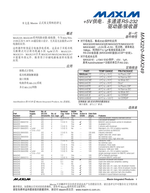
实用文档特点■两路全桥,最大输出电流. 1.3 A(R DSON = 500 mΩ)■带查表功能的可编程驱动电流曲线表格: 9 级5位精度■内置PWM电流调整器和电流传感器■可编程的步进模式:全步、半步、细步、微步■可编程摆率控制:改善EMC性能降低功耗■可编程的高速-, 低速-,混合- 和自动衰减模式■ 3位精度的全范围可编程电流■可编程堵转检测■降低对微处理器要求的步进时钟输入■待机模式下功耗很低IS < 3 μA, typ. Tj ≤85 °C■所有输出均带:短路保护,负载开路,过载,温度预警和热关断功能■内部PWM控制器的PWM信号可以当做数据输出使用。
.■在下列工作范围内所有指标都会保证3 V < Vcc <5.3 V and for 7 V < Vs < 20 V用途双极步进电机驱动器在汽车上的应用:如灯光的水平控制,灯光方向调整,节气门控制。
描述L9942是一款集成的双极步进电机驱动器,具有细分模式和可编程电流配置表,能灵活适应步进电机的特性和预期的工作情况。
可以根据目标情况选用不同的电流配置表:噪音,振动,转速或者转矩。
衰减模式用在PWM-电流控制电路中,可以编程设置成低速-,高速-,混合-和自动衰减模式。
在自动衰减模式下,如果下一步电流是增加的,器件会采用低速模式,如果下一步电流是衰减的,则会采用高速或者混合模式。
可编程堵转检测在前灯水平调整和弯道调整应用中非常有用,可以防止堵转时电机为了转到位置而长时间的运行。
如果检测到堵转,对准过程被关闭,并且噪声被最小化。
表1 器件概要2009年5月文档编号11778 Rev6目录1 框图与引脚 . . . . . . . . . . . . . . . . . . . . . . . . . . . . . . . . . . . . . . . . . . . . . . . . . . . . . . . . . . . . 62 器件描述 . . . . . . . . . . . . . . . . . . . . . . . . . . . . . . . . . . . . . . . . . . . . . . . . . . . . . . . . . . . . . . 92.3 诊断功能 . . . . . . . . . . . . . . . . . . . . . . . . . . . . . . . . . . . . . . . . . . . . . . . . . . . . . . . . . . . . 9 2.4 过压与欠压检测 . . . . . . . . . . . . . . . . . . . . . . . . . . . . . . . . . . . . . . . . . . . . . . . . . . . . . . 9 2.5 温度报警与热关断 . . . . . . . . . . . . . . . . . . . . . . . . . . . . . . . . . . . . . . . . . . . . . . . . . . . . 10 2.6 感性负载 . . . . . . . . . . . . . . . . . . . . . . . . . . . . . . . . . . . . . . . . . . . . . . . . . . . . . . . . . . 10 2.7 交叉电流保护 . . . . . . . . . . . . . . . . . . . . . . . . . . . . . . . . . . . . . . . . . . . . . . . . . . . . . . . 10 2.8 PWM 电流调整 . . . . . . . . . . . . . . . . . . . . . . . . . . . . . . . . . . . . . . . . . . . . . . . . . . . . . . 10 2.9 衰减模式 . . . . . . . . . . . . . . . . . . . . . . . . . . . . . . . . . . . . . . . . . . . . . . . . . . . . . . . . . . . 10 2.10 过流检测 . . . . . . . . . . . . . . . . . . . . . . . . . . . . . . . . . . . . . . . . . . . . . . . . . . . . . . . . . 11 2.11 负载开路检测 . . . . . . . . . . . . . . . . . . . . . . . . . . . . . . . . . . . . . . . . . . . . . . . . . . . . . . 11 2.12 步进模式 . . . . . . . . . . . . . . . . . . . . . . . . . . . . . . . . . . . . . . . . . . . . . . . . . . . . . . . . . . 112.13 衰减模式 . . . . . . . . . . . . . . . . . . . . . . . . . . . . . . . . . . . . . . . . . . . . . . . . . . . . . . . . . . 133 电气参数 . . . . . . . . . . . . . . . . . . . . . . . . . . . . . . . . . . . . . . . . . . . . . . . . . . . . . . . . . . . . 14 3.1 绝对最大额定值 . . . . . . . . . . . . . . . . . . . . . . . . . . . . . . . . . . . . . . . . . . . . . . . . . . . . . 14 3.2 ESD 静电保护 . . . . . . . . . . . . . . . . . . . . . . . . . . . . . . . . . . . . . . . . . . . . . . . . . . . . . . 14 3.3 热参数 . . . . . . . . . . . . . . . . . . . . . . . . . . . . . . . . . . . . . . . . . . . . . . . . . . . . . . . . . . . . . 15 3.4 电气特性 . . . . . . . . . . . . . . . . . . . . . . . . . . . . . . . . . . . . . . . . . . . . . . . . . . . . . . . . . . . 16 3.4.1 电源 . . . . . . . . . . . . . . . . . . . . . . . . . . . . . . . . . . . . . . . . . . . . . . . . . . . . . . . . . . . . . 16 3.4.2 过压和欠压检测 . . . . . . . . . . . . . . . . . . . . . . . . . . . . . . . . . . . . . . . . . . . . . . . . . . . . 17 3.4.3 参考电流输出 . . . . . . . . . . . . . . . . . . . . . . . . . . . . . . . . . . . . . . . . . . . . . . . . . . . . . . 17 3.4.4 电荷泵输出 . . . . . . . . . . . . . . . . . . . . . . . . . . . . . . . . . . . . . . . . . . . . . . . . . . . . . . . 18 3.4.5 输出: Qxn (x = A; B n = 1; 2) . . . . . . . . . . . . . . . . . . . . . . . . . . . . . . . . . . . . . . . . . . 183.4.6 PWM 控制 . . . . . . . . . . . . . . . . . . . . . . . . . . . . . . . . . . . . . . . . . . . . . . . . . . . . . . . . 204 SPI的逻辑功能描述 . . . . . . . . . . . . . . . . . . . . . . . . . . . . . . . . . . . . . . . . . . . . . . . . . . . . 21 4.1 电机步进时钟输入 (STEP) . . . . . . . . . . . . . . . . . . . . . . . . . . . . . . . . . . . . . . . . . . . . . 21 4.2 PWM 输出 (PWM) . . . . . . . . . . . . . . . . . . . . . . . . . . . . . . . . . . . . . . . . . . . . . . . . . . . 21 4.3 串行外设接口 (SPI) . . . . . . . . . . . . . . . . . . . . . . . . . . . . . . . . . . . . . . . . . . . . . . . . . . 214.4 芯片反相片选 (CSN) . . . . . . . . . . . . . . . . . . . . . . . . . . . . . . . . . . . . . . . . . . . . . . . . 21 4.5 串行数据输入 (DI) . . . . . . . . . . . . . . . . . . . . . . . . . . . . . . . . . . . . . . . . . . . . . . . . . . 21 4.6 串行数据输出 (DO) . . . . . . . . . . . . . . . . . . . . . . . . . . . . . . . . . . . . . . . . . . . . . . . . . 22 4.7 串行时钟 (CLK) . . . . . . . . . . . . . . . . . . . . . . . . . . . . . . . . . . . . . . . . . . . . . . . . . . . . 224.8 数据寄存器 . . . . . . . . . . . . . . . . . . . . . . . . . . . . . . . . . . . . . . . . . . . . . . . . . . . . . . . 225 SPI –控制和状态寄存器 . . . . . . . . . . . . . . . . . . . . . . . . . . . . . . . . . . . . . . . . . . . . . . . 235.3 寄存器 2 . . . . . . . . . . . . . . . . . . . . . . . . . . . . . . . . . . . . . . . . . . . . . . . . . . . . . . . . . 24 5.4 寄存器 3 . . . . . . . . . . . . . . . . . . . . . . . . . . . . . . . . . . . . . . . . . . . . . . . . . . . . . . . . . 25 5.5 寄存器 4 和 5 . . . . . . . . . . . . . . . . . . . . . . . . . . . . . . . . . . . . . . . . . . . . . . . . . . . . . 25 5.6 寄存器 6 . . . . . . . . . . . . . . . . . . . . . . . . . . . . . . . . . . . . . . . . . . . . . . . . . . . . . . . . . 26 5.7 寄存器 7 . . . . . . . . . . . . . . . . . . . . . . . . . . . . . . . . . . . . . . . . . . . . . . . . . . . . . . . . . 26 5.8 辅助逻辑模块 . . . . . . . . . . . . . . . . . . . . . . . . . . . . . . . . . . . . . . . . . . . . . . . . . . . . . 27 5.8.1 故障条件 . . . . . . . . . . . . . . . . . . . . . . . . . . . . . . . . . . . . . . . . . . . . . . . . . . . . . . . . 27 5.8.2 SPI 通讯监视 . . . . . . . . . . . . . . . . . . . . . . . . . . . . . . . . . . . . . . . . . . . . . . . . . . . . 275.8.3 用于堵转检测的PWM 监视 . . . . . . . . . . . . . . . . . . . . . . . . . . . . . . . . . . . . . . . . . 276 SPI 逻辑的电气特性 . . . . . . . . . . . . . . . . . . . . . . . . . . . . . . . . . . . . . . . . . . . . . . . . 28 6.1 输入: CSN, CLK, STEP, EN 和 DI . . . . . . . . . . . . . . . . . . . . . . . . . . . . . . . . . . . . . 28 6.2 DI 的时序 . . . . . . . . . . . . . . . . . . . . . . . . . . . . . . . . . . . . . . . . . . . . . . . . . . . . . . . . 28 6.3 输出: DO, PWM . . . . . . . . . . . . . . . . . . . . . . . . . . . . . . . . . . . . . . . . . . . . . . . . . . . 29 6.4 输出: DO 的时序 . . . . . . . . . . . . . . . . . . . . . . . . . . . . . . . . . . . . . . . . . . . . . . . . . . . 29 6.5 CSN 的时序 . . . . . . . . . . . . . . . . . . . . . . . . . . . . . . . . . . . . . . . . . . . . . . . . . . . . . . 296.6 STEP 的时序 . . . . . . . . . . . . . . . . . . . . . . . . . . . . . . . . . . . . . . . . . . . . . . . . . . . . . 307 附录 . . . . . . . . . . . . . . . . . . . . . . . . . . . . . . . . . . . . . . . . . . . . . . . . . . . . . . . . . . . . . 337.1 堵转检测 . . . . . . . . . . . . . . . . . . . . . . . . . . . . . . . . . . . . . . . . . . . . . . . . . . . . . . . . 337.2 步进时钟输入 . . . . . . . . . . . . . . . . . . . . . . . . . . . . . . . . . . . . . . . . . . . . . . . . . . . . . 337.3 负载电流控制和过流检测(输出短路) . . . . . . . . . . . . . . . . . . . . . . . . . . . . . . . . . 338 包装信息 . . . . . . . . . . . . . . . . . . . . . . . . . . . . . . . . . . . . . . . . . . . . . . . . . . . . . . . . 389 历史版本 . . . . . . . . . . . . . . . . . . . . . . . . . . . . . . . . . . . . . . . . . . . . . . . . . . . . . . . . . 39表格列表表 1. 器件概要 . . . . . . . . . . . . . . . . . . . . . . . . . . . . . . . . . . . . . . . . . . . . . . . . . . . . . . . . . . 1 表 2. 引脚描述 . . . . . . . . . . . . . . . . . . . . . . . . . . . . . . . . . . . . . . . . . . . . . . . . . . . . . . . . . . 7 表 3. 真值表 . . . . . . . . . . . . . . . . . . . . . . . . . . . . . . . . . . . . . . . . . . . . . . . . . . . . . . . . . . . . 11 表 4. 绝对最大额定值 . . . . . . . . . . . . . . . . . . . . . . . . . . . . . . . . . . . . . . . . . . . . . . . . . . . . . 14 表 5. ESD 静电保护 . . . . . . . . . . . . . . . . . . . . . . . . . . . . . . . . . . . . . . . . . . . . . . . . . . . . . . 14 表 6. 工作时的结温 . . . . . . . . . . . . . . . . . . . . . . . . . . . . . . . . . . . . . . . . . . . . . . . . . . . . . . . 15表 9. 过压和欠压检测 . . . . . . . . . . . . . . . . . . . . . . . . . . . . . . . . . . . . . . . . . . . . . . . . . . . . . 17 表 10. 参考电流输出 . . . . . . . . . . . . . . . . . . . . . . . . . . . . . . . . . . . . . . . . . . . . . . . . . . . . . . 17 表 11. 电荷泵输出 . . . . . . . . . . . . . . . . . . . . . . . . . . . . . . . . . . . . . . . . . . . . . . . . . . . . . . . . 18 表 12. 输出: Qxn (x = A; B n =1; 2) . . . . . . . . . . . . . . . . . . . . . . . . . . . . . . . . . . . . . . . . . . 18 表 13. PWM 控制 (见图 4 和图 7). . . . . . . . . . . . . . . . . . . . . . . . . . . . . . . . . . . . . . . . . . . 20 表 14. 寄存器 0 . . . . . . . . . . . . . . . . . . . . . . . . . . . . . . . . . . . . . . . . . . . . . . . . . . . . . . . . . . 23 表 15. 寄存器 1 . . . . . . . . . . . . . . . . . . . . . . . . . . . . . . . . . . . . . . . . . . . . . . . . . . . . . . . . . . 24 表 16. 寄存器 2 . . . . . . . . . . . . . . . . . . . . . . . . . . . . . . . . . . . . . . . . . . . . . . . . . . . . . . . . . . 24 表 17. 寄存器 3 . . . . . . . . . . . . . . . . . . . . . . . . . . . . . . . . . . . . . . . . . . . . . . . . . . . . . . . . . . 25 表 18. 寄存器 4 和 5 . . . . . . . . . . . . . . . . . . . . . . . . . . . . . . . . . . . . . . . . . . . . . . . . . . . . . . 25 表 19. 寄存器 6 . . . . . . . . . . . . . . . . . . . . . . . . . . . . . . . . . . . . . . . . . . . . . . . . . . . . . . . . . . 26 表 20. 寄存器 7 . . . . . . . . . . . . . . . . . . . . . . . . . . . . . . . . . . . . . . . . . . . . . . . . . . . . . . . . . . 26 表 21. 输入: CSN, CLK, STEP, EN and DI . . . . . . . . . . . . . . . . . . . . . . . . . . . . . . . . . . . . . 28 表 22. DI 的时序 (见图 11 和图 13) . . . . . . . . . . . . . . . . . . . . . . . . . . . . . . . . . . . . . . . . . . 28 表 23. 输出: DO, PWM . . . . . . . . . . . . . . . . . . . . . . . . . . . . . . . . . . . . . . . . . . . . . . . . . . . . 29 表 24. 输出: DO 的时序(见图 12 和图 13) . . . . . . . . . . . . . . . . . . . . . . . . . . . . . . . . . . . . . . 29 表 25. CSN 的时序 . . . . . . . . . . . . . . . . . . . . . . . . . . . . . . . . . . . . . . . . . . . . . . . . . . . . . . . 29 表 26. STEP 的时序 . . . . . . . . . . . . . . . . . . . . . . . . . . . . . . . . . . . . . . . . . . . . . . . . . . . . . . . 30 表 27. 文档历史版本 . . . . . . . . . . . . . . . . . . . . . . . . . . . . . . . . . . . . . . . . . . . . . . . . . . . . . . . 39插图列表图 1. 方框图. . . . . . . . . . . . . . . . . . . . . . . . . . . . . . . . . . . . . . . . . . . . . . . . . . . . . . . . . . . . 6图 2. 引脚图 (顶视) . . . . . . . . . . . . . . . . . . . . . . . . . . . . . . . . . . . . . . . . . . . . . . . . . . . . . . 6图 3. 步进模式 . . . . . . . . . . . . . . . . . . . . . . . . . . . . . . . . . . . . . . . . . . . . . . . . . . . . . . . . . 12图 4. 衰减模式 . . . . . . . . . . . . . . . . . . . . . . . . . . . . . . . . . . . . . . . . . . . . . . . . . . . . . . . . . 13图 5. 封装的热数据 . . . . . . . . . . . . . . . . . . . . . . . . . . . . . . . . . . . . . . . . . . . . . . . . . . . . . 15图 6. VS 监视 . . . . . . . . . . . . . . . . . . . . . . . . . . . . . . . . . . . . . . . . . . . . . . . . . . . . . . . . . . 17图 7. 设置负载电流限制的逻辑 . . . . . . . . . . . . . . . . . . . . . . . . . . . . . . . . . . . . . . . . . . . . . 19图 8. 最小切换时间 . . . . . . . . . . . . . . . . . . . . . . . . . . . . . . . . . . . . . . . . . . . . . . . . . . . . . . 20图 11. 输入时序 . . . . . . . . . . . . . . . . . . . . . . . . . . . . . . . . . . . . . . . . . . . . . . . . . . . . . . . . . 30 图 12. SPI - DO 有效的数据延迟时间和有效时间 . . . . . . . . . . . . . . . . . . . . . . . . . . . . . . . 31 图 13. DO 使能和禁止时间 . . . . . . . . . . . . . . . . . . . . . . . . . . . . . . . . . . . . . . . . . . . . . . . . 31 图 14. 状态位 0 的时序 (故障条件) . . . . . . . . . . . . . . . . . . . . . . . . . . . . . . . . . . . . . . . . . . 32 图 15. 堵转检测 . . . . . . . . . . . . . . . . . . . . . . . . . . . . . . . . . . . . . . . . . . . . . . . . . . . . . . . . . 35 图 16. PWM 控制的参考产生 (接通) . . . . . . . . . . . . . . . . . . . . . . . . . . . . . . . . . . . . . . . . . 36 图 17. PWM控制的参考产生 (衰减) . . . . . . . . . . . . . . . . . . . . . . . . . . . . . . . . . . . . . . . . . . 37 图 18. PowerSSO24 机械尺寸和包装规格 . . . . . . . . . . . . . . . . . . . . . . . . . . . . . . . . . . . . 381 框图与引脚图图 1. 框图图 2. 引脚图 (顶视)2 芯片描述2.1 双电源供电: VS 和 VCC电源引脚VS脚给半桥供电。


FEATURES♦Silicon Planar Zener Diodes♦In Mini-MELF case especially for automatic insertion.♦The Zener voltages are graded according to the international E 24 standard. Smaller voltagetolerances and other Zener voltages are available upon request.♦These diodes are also available in DO-35 case with the type designation ZPD1 … ZPD51.MECHANICAL DATACase:Mini-MELF Glass Case (SOD-80)Weight:approx. 0.05 gMAXIMUM RATINGSRatings at 25°C ambient temperature unless otherwise specified.SYMBOL VALUE UNITZener Current (see Table “Characteristics”)Power Dissipation at T amb = 25°C P tot 500(1)mW Junction Temperature T j 175°C Storage Temperature RangeT S– 55 to +175°CZENER DIODES.142 (3.6).019 (0.48)∅Cathode Mark.063 (1.6).134 (3.4).055 (1.4).011 (0.28)Dimensions are in inches and (millimeters)ZMM1(3)0.7 ... 0.8 6.5 (< 8)< 50– 26 ... – 23–280340ZMM2.7 2.5 ... 2.975 (< 83)< 500– 9 ... – 4–135160ZMM3 2.8 ... 3.280 (< 95)< 500– 9 ... – 3–117140ZMM3.3 3.1 ... 3.580 (< 95)< 500– 8 ... – 3–109130ZMM3.6 3.4 ... 3.880 (< 95)< 500– 8 ... – 3–101120ZMM3.9 3.7 ... 4.180 (< 95)< 500– 7 ... – 3–92110ZMM4.3 4.0 ... 4.680 (< 95)< 500– 6 ... – 1–85100ZMM4.7 4.4 ... 5.070 (< 78)< 500– 5 ... +2–7690ZMM5.1 4.8 ... 5.430 (< 60)< 480– 3 ... +4> 0.86780ZMM5.6 5.2 ... 6.010 (< 40)< 400– 2 ... +6> 15970ZMM6.2 5.8 ... 6.6 4.8 (< 10)< 200– 1 ... +7> 25464ZMM6.8 6.4 ... 7.2 4.5 (< 8)< 150+2 ... +7> 34958ZMM7.57.0 ... 7.9 4 (< 7)< 50+3 ... +7> 54453ZMM8.27.7 ... 8.7 4.5 (< 7)< 50+4 ... +7> 64047ZMM9.18.5 ... 9.6 4.8 (< 10)< 50+5 ... +8> 73643ZMM109.4 ... 10.6 5.2 (< 15)< 70+5 ... +8> 7.53340ZMM1110.4 ... 11.6 6 (< 20)< 70+5 ... +9> 8.53036ZMM1211.4 ... 12.77 (< 20)< 90+6 ... +9> 92832ZMM1312.4 ... 14.19 (< 25)< 110+7 ... +9> 102529ZMM1513.8 ... 15.611 (< 30)< 110+7 ... +9> 112327ZMM1615.3 ... 17.113 (< 40)< 170+8 ... +9.5> 122024ZMM1816.8 ... 19.118 (< 50)< 170+8 ... +9.5> 141821ZMM2018.8 ... 21.220 (< 50)< 220+8 ... +10> 151720ZMM2220.8 ... 23.325 (< 55)< 220+8 ... +10> 171618ZMM2422.8 ... 25.628 (< 80)< 220+8 ... +10> 181316ZMM2725.1 ... 28.930 (< 80)< 250+8 ... +10> 201214ZMM3028 ... 3235 (< 80)< 250+8 ... +10> 22.51013ZMM3331 ... 3540 (< 80)< 250+8 ... +10> 25912ZMM3634 ... 3840 (< 90)< 250+8 ... +10> 27911ZMM3937 ... 4150 (< 90)< 300+10 ... +12> 29810ZMM4340 ... 4660 (< 100)< 700+10 ... +12> 3279.2ZMM4744 ... 5070 (< 100)< 750+10 ... +12> 3568.5ZMM5148 (54)70 (< 100)< 750+10 ... +12> 3867.8ZMM5652.0 … 60.0(4)<135(4)<1000(5)typ. +10(4)–––ZMM6258.0 … 66.0(4)<150(4)<1000(5)typ. +10(4)–––ZMM6864.0 … 72.0(4)<200(4)<1000(5)typ. +10(4)–––ZMM7570.0 … 79.0(4)<250(4)<1500(5)typ. +10(4)–––NOTES:(1) Tested with pulses t p = 5 ms(2) Valid provided that electrodes are kept at ambient temperature(3) The ZMM1 is a silicon diode operated in forward direction. Hence, the index of all parameters should be “F” instead of “Z”Connect the cathode electrode to the negative pole (4) at I Z = 2.5 mA (5) at I Z = 0.5 mAELECTRICAL CHARACTERISTICSRatings at 25°C ambient temperature unless otherwise specified.TypeZener Voltage (1)at I Z = 5 mAV Z Vat I Z = 5 mA f = 1 kHz r zj Ωat I Z = 1 mA f = 1 kHz r zj ΩTemp. Coeff.of Zener Voltageat I Z = 5 mA αVZ 10–4/K Reverse Voltage atI R = 100 nAV R V atT amb = 45°C I Z = mA Admissable Zener current (2)atT amb = 25°C I Z = mA Dynamic Resistance。


Commercial productsSERIESIn addition to being the most recognized brand of hub on the market, Myers™ offers largerstainless hub trade sizes, aluminum hubs, ATEX approved hubs, cap-offs, drains, and more!The original!Often imitated, never duplicated! Available in a wide range of sizes, materials and ratings to meet virtually any customer application!2 EATON’S CROUSE-HINDSEATON’S CROUSE-HINDS 3-55°C to 180°CATEX rated hubHub is listed for use in hazardous (classified) locations to IECEx-ATEXcertifications. Ideal for global requirements and OEM’s shipping material worldwide.Ground hubCombines all of the features of the Hub Basic Scru-Tite plus the additional feature of the grounding screw on the locknut.Hub Basic Scru-Tite™Hubs are ideal for general use with rigid conduit. Provides positive seal and electrical ground.Through-bulkhead fittingHubs are the perfect method for installing hubs on cast boxes or through thicker walls.Drain plugsDesigned to install in the bottom of an enclosure to drain any accumulated condensation. Available in aluminum or stainless steel construction.Cap-offDesigned to install in enclosure to provide environmental cap for unused entries or knockouts.Metric to NPT adapterUsed to convert a threaded metric entryto a NPT entry.Available in trade sizes 3/8” through 6” Available in trade sizes 1/2” through 6” Available in trade sizes 1/2” through 4”Myers hubs design featuresVibration-proof• Strong, oversize nut with radial serrations helps assure flush installation and positive grounding1Grounding screw •For added safetyCaptive o-ring gasket• Impervious to corrosive moisture and petroleum products. Gasket helps assure positive water and dust-tight installations4Precision machine cut threads • 5No welding• Unique serrations on both nut approved for use with service entrance conduit)Posi-lok insulated throat• Cannot come out, standard in sizes from 1/2” through 4”4 EATON’S CROUSE-HINDSApplications:• Myers hubs are used in the termination of electrical circuits through wall of the enclosure • Designed for use indoors or outdoors with rigid conduit and IMC • I deal for pharmaceutical, chemical and food processing, pulp/paper, nuclear, solar and commercial construction applications • Suitable for use in environmentally demanding applications, including those with the presence of chemicals, such as acetic, citric and salt water • Suitable for use in hazardous (classified) locationsFeatures:• Wide range of styles, trade sizes and materials to meet customer requirements and preferences • Multiple certifications provide users peace of mind • Easy installation and smooth pulling service for labor savings • Tapered female threads for rigid/IMC conduit, NPSM male threadsCertification and compliances:NEC/CEC:• Class I, Division 2• Class II, Division 1 & 2• Class III, Division 1 & 2• Class I, Zone 1, AEx e II • Class I, Zone 1, Ex e II cULus Listed • UL Standard 514B• CSA Standard C22.2 No. 18NEMA Type 2, 3, 3R, 4, 4X, 12 (std & ground hub) IEC:STGK:• ATEX Certified ITS12ATEX47591X Ex II 2G Ex e IIC Gb to EN 60079-0:2009, EN 60079-7:2007, and EN 60079-14 Standards Ta -15°C to 120°C • IECEx Certified IECEx ETL 12.0009X Ex e IIC Gb to IEC 60079-0:2007-10, Edition 5, IEC 60079-7:2006-07, Edition 4 and IEC 60079-14 Standards Ta -15°C to 120°C • IP66SSTGK M2:• ATEX Certified DEMKO 18 ATEX 2002X, II 2G Ex eb IIC Gb to EN IEC 60079-0:2018 and EN IEC 60079-7:2015 +A1:2018 standards Ta -55°C to 180°C • IECEx Certified IECEx UL 18.0007X, Ex eb IIC Gb to IEC 60079-0:2017 and IEC 60079-7:2017 standards Ta -55°c to 180°C • IP66Standard materials:• Nut: zinc (Zamek-2, Zamek-3), aluminum (Al 360), stainless (316)• Body: zinc (Zamek-2, Zamek-3), aluminum (Al 360), stainless (316)• Insuliner: Lexan, PEEK GF15 (SSTGK M2 only)• O-Ring: Viton; silicone (SSTGK M2 only)• Ground screw: Steel/stainless steelStandard finishes:• Aluminum: natural • Zinc: natural • Stainless: naturalMyers hubsOptions:Description• Nickel-chrome plate finish (zinc hubs only)CPEATON’S CROUSE-HINDS 5Myers hubsHub basic Scru-TiteNEMA 2, 3, 3R, 4, 4X, 12ZincUL File No. E-27258†Optional nickel-chrome plate finish. Add suffix -CP.*Not supplied with insulator.Cat. #SizeUnit qty.Wt. lbs. per 100ST 03†3/”2511ST 12*6”1685*Not supplied with insulator.‡Use of wire terminal is required by CSA and recommended by UL for wire gauges over 10 AWG.Cat. #SizeUnit qty.Wt. lbs. per 100Max. copper ground wire size CSA‡UL‡STG 11/”2520#8#8Ground hubNEMA 2, 3, 3R, 4, 4X, 12ZincUL File No. E-59509Hub basic Scru-TiteNEMA 2, 3, 3R, 4, 4X, 12AluminumUL File No. E-27258*Not supplied with insulator.Cat. #SizeUnit qty.Wt. lbs. per 100STA 11/”258Cat. #SizeUnit qty.Wt. lbs. per 100SSTG 11/”1029Ground hubNEMA 2, 3, 3R, 4, 4X, 12316 stainless steelUL File No. E-59509**Not UL Listed as a means of grounding and bonding. Does not include tapped ground tabor ground screw.Cat. #SizeUnit qty.Wt. lbs. per 10016 EATON’S CROUSE-HINDSMyers hubsGround hubNEMA 2, 3, 3R, 4, 4X, 12AluminumUL File No. E-59509*Not supplied with insulator.‡Use of wire terminal is required by CSA and recommended by UL for wire gauges over 10 AWG.Cat. #SizeUnit qty.Wt. lbs. per 100Max. copper ground wire size CSA‡UL‡STAG 11/”2513#8#8ATEX hazardous location hub with increased safety ground terminalNEMA 2, 3, 3R, 4, 4X; IP66ZincII 2 G Ex e IIC Gb Ta (-15°C to 120°C) IECEx – Ex e IIC Gb Ta (-15°C to 120°C)Class I, Zone 1, AEx e II Class I, Zone 1, Ex e II UL File No. E-59509‡Use of wire terminal is required by CSA and recommended by UL for wire gauges over 10 AWG.Cat. #SizeUnit qty.Wt. lbs. per 100Max. copper ground wire size CSA‡UL‡STGK 11/”1020#8#8ATEX hazardous location hub with increased safety ground terminalNEMA 2, 3, 3R, 4, 4X; IP66316 stainless steelII 2 G Ex eb IIC Gb Ta (-55°C to 180°C)IECEx – Ex eb IIC Gb Ta (-55°C to 180°C)Class I, Zone 1, AEx e IIClass I, Zone 1, Ex e IIUL File No. E-187273Cat. #SizeUnit qty.Wt. lbs. per 100Max. copper ground wire size CSA‡UL‡SSTGK 1 M21/”1033#8#8‡Use of wire terminal is required by CSA and recommended by UL for wire gauges over10 AWG.**Not UL Listed as a means of grounding and bonding.EATON’S CROUSE-HINDS 7Cat. #SizeUnit qty.Wt. lbs. per 100STTB 11/”530Through-bulkhead fittingZincUL File No. E-27258Myers hubsCat. #SizeUnit qty.Wt. lbs. per 100STTBA 11/”511Through-bulkhead fittingAluminumUL File No. E-27258Cat. #SizeUnit qty.Wt. lbs. per 100STTTB 11/”535Through-bulkhead fittingZinc without nipplesPackaged as two pieces unassembledUL File No. E-27258Cat. #SizeUnit qty.Wt. lbs. per 100STTTBA 11/”516Through-bulkhead fittingAluminum without nipplesPackaged as two pieces unassembledUL File No. E-27258Note: T he Myers metric to NPT hub adapter is used to convert a threaded metric entry toan NPT entry. The female thread is NPT and the male thread is metric.Cat. #SizeUnit qty.Wt. lbs. per 100STM 1M20 - 1/” 2513Metric to NPT adapterZinc8 EATON’S CROUSE-HINDSMyers hubsNon-hazardous drain plug316 stainless steelUL File No. E-23223†Optional nickel-chrome plate finish. Add suffix -CP.*Not UL Listed.Cat. #SizeUnit qty.Wt. lbs. per 100SSTC 11/” 2517SSTC 1SSTC 1CDNote: S STC 1 and STAC 1ST are for knockouts and are supplied with a locknut and straightthreads. SSTC 1CD and STAC 1CD are for threaded openings and are supplied without locknut and NPT threads. Not gasketed to allow for water drainage.Cat. #SizeUnit qty.Wt. lbs. per 100STAC 1ST 1/” 256Non-hazardous drain plugAluminumUL File No. E-23223STAC 1STSTAC 1CDCap-offZincUL File No. E-23223Cat. #SizeUnit qty.Wt. lbs. per 100STC 1†1/” 2513Cat. #SizeUnit qty.Wt. lbs. per 100STAC 11/” 255STAC 31”2512Cap-offAluminumUL File No. E-23223‡Use of wire terminal is required by CSA and recommended by UL for wire gauges over 10 AWG.Cat. #SizeUnit qty.Wt. lbs. per 100Max. copper ground wire size CSA‡UL‡STGN 11/”256#8#8Ground NutZincUL File No. E-59509Cat. #SizeUnit qty.Wt. lbs. per 100Max. copper ground wire size CSA‡UL‡STAGN 11/”253#8#8‡Use of wire terminal is required by CSA and recommended by UL for wire gauges over10 AWG.Ground NutAluminumUL File No. E-59509EATON’S CROUSE-HINDS 9Hub dimensions (in inches):“D” dimension indicates maximum panel thickness which hub will accommodate.Pipe SizeABCDEFGHK (Mounting Hole)Min.Max.Min.Max.3/13/11/21/1/0.4680.4933/ NPT 3/ NPSM 60°43/11/637/162/165.7626.065 6 NPT6 NPSM45°6/646/4Bulkhead dimensions (in inches):Cat. #SizeABHMNSTTB 1STTBA 1STTTB 11/2 1.465 1.42960°1/2 - 14 NPSM1/2 - 14 NPTMyers hubs technical information10 EATON’S CROUSE-HINDSSpacing chart:Conduit or pipe sizeMinimum space from center of pipe or conduit to nearest obstruction Myers hubs technical informationNotes___________________________________________________ ___________________________________________________ ___________________________________________________ ___________________________________________________ ___________________________________________________ ___________________________________________________ ___________________________________________________ ___________________________________________________ ___________________________________________________ ___________________________________________________ ___________________________________________________ ___________________________________________________ ___________________________________________________ ___________________________________________________ ___________________________________________________ ___________________________________________________ ___________________________________________________ ___________________________________________________ ___________________________________________________ ___________________________________________________ ___________________________________________________ ___________________________________________________ ___________________________________________________ ___________________________________________________EATON’S CROUSE-HINDS 11Eaton 1000 Eaton Boulevard Cleveland, OH 44122United States © 2022 Eaton Corporation All Rights Reserved Printed in USA Form No. BR406001EN June 2022Eaton’s Crouse-Hinds Division 1201 Wolf Street Syracuse, NY 13208(866) 764-5454***************************Eaton is a registered trademark.All other trademarks are property of their respective owners.India 91-124-4683888 FAX: 91-124-4683899******************Australia 61-2-8787-2777 FAX: 61-2-9609-2342************************Korea 82-2-3484-6783 82-2-3484-6778*******************China 86-21-2899-3600 FAX: 86-21-2899-4055******************Singapore 65-6645-9888 FAX: 65-6297-4819********************Eaton Middle East 9714-8066100 FAX: 9714-8894813*******************Europe (Germany)49 (0) 6271 806-500 49 (0) 6271 806-476****************Mexico/Latin America/Caribbean 52-555-804-4000 FAX: 52-555-804-4020*************************Canada Toll Free: 800-265-0502 FAX: (800) 263-9504 FAX Orders only: (866) 653-0645U.S. (global headquarters): Eaton's Crouse-Hinds, B-Line and Oil and Gas business 1201 Wolf Street Syracuse, NY 13208(866) 764-5454 FAX: (315) 477-5179 FAX Orders Only: (866) 653-0640***************************。


HANBit HMD32M32M16GGENERAL DESCRIPTIONThe HMD32M32M16G is a 32M x 32bit dynamic RAM high-density memory module. The module consists of sixteen CMOS 16M x 4bit DRAMs in 32-pin TSOPII packages mounted on a 72-pin, double-sided, FR-4-printed circuit board. A 0.1uF decoupling capacitor is mounted on the printed circuit board for each DRAM components. The module is a Single In-line Memory Module with edge connections and is intended for mounting in to 72-pin edge connector sockets. All module components may be powered from a single 5V DC power supply and all inputs and outputs are TTL-compatible.FEATURESw Part IdentificationHMD32M32M16G-- 4K Cycles/64ms Ref. Gold w Access times : 50, 60nsw High-density 128MByte designw Single + 5V ±0.5V power supplyw JEDEC standard pinoutw Fast Page mode operationw TTL compatible inputs and outputsw FR4-PCB designOPTIONS MARKINGw Timing50ns access -560ns access -6w Packages72-pin SIMM MPERFORMANCE RANGESPEED tRAC tCAC tRC-5 50ns 13ns 90ns-6 60ns 15ns 110nsPRESENCE DETECT PINSPin 50ns 60nsPD1 NC NCPD2 Vss VssPD3 Vss NCPD4 Vss NC PIN SYMBOL PIN SYMBOL PIN SYMBOL1 Vss 25 DQ22 49 DQ82 DQ0 26 DQ7 50 DQ243 DQ16 27 DQ23 51 DQ94 DQ1 28 A7 52 DQ255 DQ17 29 A11 53 DQ106 DQ2 30 Vcc 54 DQ267 DQ18 31 A8 55 DQ118 DQ3 32 A9 56 DQ279 DQ19 33 /RAS3 57 DQ1210 Vcc 34 /RAS2 58 DQ2811 NC 35 NC 59 Vcc12 A0 36 NC 60 DQ2913 A1 37 NC 61 DQ1314 A2 38 NC 62 DQ3015 A3 39 Vss 63 DQ1416 A4 40 /CAS0 64 DQ3117 A5 41 /CAS2 65 DQ1518 A6 42 /CAS3 66 NC19 A10 43 /CAS1 67 PD120 DQ4 44 /RAS0 68 PD221 DQ20 45 /RAS1 69 PD322 DQ5 46 NC 70 PD423 DQ21 47 /WE 71 NC24 DQ6 48 NC 72 VssPIN ASSIGNMENT72 PIN SIMM TOP VIEWHANBit HMD32M32M16G FUNCTIONAL BLOCK DIAGRAM/RAS3Vss 0.1uF Capacitorfor each DRAM To all DRAMs/CAS0/RAS1/CAS1/CAS2/CAS3VccHANBit HMD32M32M16G ABSOLUTE MAXIMUM RATINGSPARAMETER SYMBOL RATINGVoltage on Any Pin Relative to Vss V IN ,OUT-1V to 7.0VVoltage on Vcc Supply Relative to Vss Vcc -1V to 7.0VPower Dissipation P D16WStorage Temperature T STG-55o C to 150o CShort Circuit Output Current I OS50mAw Permanent device damage may occur if " Absolute Maximum Ratings" are exceeded. Functional operation should be restricted to the conditions as detailed in the operational sections of this data sheet. Exposure to absolute maximum rating conditions for extended periods may affect device reliability.RECOMMENDED DC OPERATING CONDITIONS( Voltage reference to V SS, T A=0 to 70 o C )PARAMETER SYMBOL MIN TYP. MAX UNIT Supply Voltage Vcc 4.5 5.0 5.5 V Ground Vss 0 0 0 V Input High Voltage V IH 2.4 - Vcc+1 V Input Low Voltage V IL-1.0 - 0.8 VDC AND OPERATING CHARACTERISTICSSYMBOL SPEED MIN MAX UNITS-5 - 1920 mAI CC1-6 - 1760 mAI CC2Don’t care - 32 mA-5 - 1920 mAI CC3-6 - 1760 mA-5 - 1120 mAI CC4-6 - 960 mAI CC5Don’t care - 16 mA-5 - 1920 mAI CC6-6 - 1760 mAI l(L)-10 10 µAI O(L)-5 5 µAV OH 2.4 - VV OL- 0.4 VI CC1 : Operating Current * (/RAS , /CAS , Address cycling @t RC=min.)I CC2 : Standby Current ( /RAS=/CAS=V IH )I CC3 : /RAS Only Refresh Current * ( /CAS=V IH, /RAS, Address cycling @t RC=min )HANBit HMD32M32M16GI CC4 : Fast Page Mode Current * (/RAS=V IL, /CAS, Address cycling @t PC=min )I CC5 : Standby Current (/RAS=/CAS=Vcc-0.2V )I CC6 : /CAS-Before-/RAS Refresh Current * (/RAS and /CAS cycling @t RC=min )I IL : Input Leakage Current (Any input 0V ≤ V IN≤ 6.5V, all other pins not under test = 0V)I OL : Output Leakage Current (Data out is disabled, 0V ≤ V OUT ≤ 5.5VV OH : Output High Voltage Level (I OH= -5mA )V OL : Output Low Voltage Level (I OL = 4.2mA )* NOTE: I CC1, I CC3, I CC4 and I CC6 are dependent on output loading and cycle rates. Specified values are obtained with the output open. I CC is specified as an average current. In I CC1 and I CC3, address cad be changed maximum once while /RAS=V IL. In I CC4, address can be changed maximum once within one page mode cycle.CAPACITANCE( TA =25oC, Vcc = 5V, f = 1Mz )DESCRIPTION SYMBOL MIN MAX UNITS Input Capacitance (A0-A11) C IN1- 90 pF Input Capacitance (/W) C IN2- 122 pF Input Capacitance (/RAS0) C IN3- 38 pF Input Capacitance (/CAS0-/CAS3) C IN4- 38 pF Input/Output Capacitance (DQ0-31) C DQ1- 17 pFAC CHARACTERISTICS( 0 o C ≤ TA≤ 70o C , Vcc = 5V±10%, See notes 1,2.)-5 -6PARAMETER SYMBOLMIN MAX MIN MAXUNIT Random read or write cycle time t RC84 104 ns Access time from /RAS t RAC50 60 ns Access time from /CAS t CAC13 15 ns Access time from column address t AA25 30 ns/CAS to output in Low-Z t CLZ 3 3 nsOutput buffer turn-off delay t OFF 3 13 3 15 ns Transition time (rise and fall) t T 1 50 1 50 ns/RAS precharge time t RP30 40 ns/RAS pulse width t RAS50 10K 60 10K ns/RAS hold time t RSH13 15 ns/CAS hold time t CSH38 45 ns/CAS pulse width t CAS8 10K 10 10K ns/RAS to /CAS delay time t RCD20 37 20 45 ns/RAS to column address delay time t RAD15 25 15 30 ns/CAS to /RAS precharge time t CRP 5 5 nsRow address set-up time t ASR0 0 nsHANBit HMD32M32M16GRow address hold time t RAH10 10 ns Column address set-up time t ASC0 0 ns Column Address to /RAS lead time t RAL25 30 nsRead command set-up time t RCS0 0 nsRead command hold referenced to /CAS t RCH0 0 nsRead command hold referenced to /RAS t RRH0 0 nsWrite command hold time t WCH10 10 nsWrite command hold referenced to /RAS t WCR50 55 nsWrite command pulse width t WP10 10 nsWrite command to /RAS lead time t RWL13 15 nsWrite command to /CAS lead time t CWL8 10 nsData-in set-up time t DS0 0 nsData-in hold time t DH8 10 ns Refresh period t REF64 64 nsWrite command set-up time t WCS0 0 ns/CAS setup time (C-B-R refresh) t CSR 5 5 ns/CAS hold time (C-B-R refresh) t CHR10 10 ns/RAS precharge to /CAS hold time t RPC 5 5 ns NOTES1.An initial pause of 200µs is required after power-up followed by any 8 /RAS-only or /CAS-before-/RAS refresh cycles before proper device operation is achieved.2.V IH (min) and V IL (max) are reference levels for measuring timing of input signals. Transition times are measured between V IH(min) and V IL(max) and are assumed to be 5ns for all inputs.3.Measured with a load equivalent to 2TTL loads and 100pF4.Operation within the t RCD(max) limit insures that t RAC(max) can be met. t RCD(max) is specified as a reference point only. If t RCD is greater than the specified t RCD(max) limit, then access time is controlled exclusively by t CAC.5.Assumes that t RCD≥ t RCD(max)6. t AR, t WCR, t DHR are referenced to t RAD(max)7.This parameter defines the time at which the output achieves the open circuit condition and is not referenced to V OHor V OL.8. t WCS, t RWD, t CWD anf t AWD are non restrictive operating parameter.They are included in the data sheet as electrical characteristic only. If t WCS≥tWCS(min) the cycle is an early writecycle and the data out pin will remain high impedance for the duration of the cycle.9. Either t RCH or t RRH must be satisfied for a read cycle.10. These parameters are referenced to the /CAS leading edge in early write cycles and to the /W leading edge in read-write cycles.11. Operation within the t RAD(max) limit insures that t RAC(max) can be met. t RAD(max) is specified as a referencepoint only. If t RAD is greater than the specified t RAD(max) limit. then access time is controlled by t AA.AC CHARACTERISTICS( 0 o C ≤ T≤ 70o C , Vcc = 5V±10%)AHANBit HMD32M32M16G-5 -6UNIT NOTE PARAMETER SYMBOLMIN MAX MIN MAXHyper page mode cycle time t HPC20 25 ns 11 /CAS precharge time (Hyper page cycle) t CP8 10 ns/RAS pulse width (Hyper page cycle) t RASP50 200K 60 200K ns/RAS hold time from /CAS precharge t RHCP30 35 ns/W to RAS precharge time (C-B-R refresh) t WRP10 10 ns/W to RAS hold time (C-B-R refresh) t WRH10 10 nsOutput data hold time t DOH 5 5 nsOutput buffer turn off delay from /RAS t REZ 3 13 3 15 ns 6,12 Output buffer turn off delay from W t WEZ 3 13 3 15 ns 6/W to data delay t WED15 15 ns/W puls width t WPE 5 5 nsNOTES1. An initial pause of 200us is required after power-up followed by any 8 /RAS-only or /CAS-before-/RAS refreshcycles before proper device operation is achieved.2. Input voltage levels are Vih/Vil. V IH(min) and V IL(max) are reference levels for measuring timing of input signals.Transition times are measured between V IH(min) and V IL(max) and are assumed to be 5ns for all inputs.3. Measured with a load equivalent to 1 TTL loads and 100pF.4. Operation within the t RCD(max) limit insures that t RAC(max) can be met. t RCD(max) is specified as a referencepoint only. If t RCD is greater than the specified t RCD(max) limit, then access time is controlled exclusively by t CAC.5. Assumes that t RCD ≥t RCD(max).6. This parameter defines the time at which the output achieves the open circuit and is not referenced for V OH or V OL.7. t WCS is non-restrictive operating parameter. It is included in the data sheet as electrical characteristics only. Ift WCS≥ t WCS(min), the cycle is an early write cycle and the data out pin will remain high impedance for the duration of the cycle.8. Either t RCH or t RRH must be satisfied for a read cycle.9. These parameters are referenced to the /CAS leading edge in early write cycles.10. Operation within the t RAD(max) limit insures that t RAC(max) can be met. t RAD(max) is specified as reference point only. If t RAD is greater than the specified t RAD(max) limit access time is controlled by t AA.11. tASC ≥6ns, Assume t T=2.0ns.12. If /RAS goes high before /CAS high going, the open circuit condition of the output is achieved by /CAS high going.If /CAS goes high before /RAS high going , the open circuit condition of the output is achieved by /RAS going..HANBit HMD32M32M16GPACKAGING INFORMATIONORDERING INFORMATIONPart NumberDensityOrg.PackageComponent Number VccMODESPEEDHMD32M32M16G-5 128Byte x 32 72 Pin-SIMM 16EA 5V FPM 50ns HMD32M32M16G-6 128Bytex 3272 Pin-SIMM16EA5VFPM60ns0.25 mm MAX(Solder & Gold Plating)。


WAVES UM225/UM226 User GuideTABLE OF CONTENTSChapter 1 – Introduction (3)1.1 Welcome (3)1.2 Product Overview (3)1.3 Concepts and Terminology (3)1.4 Components (4)1.5 WaveSystem Toolbar (4)Chapter 2 – Quickstart Guide (5)Chapter 3 – Interface and Controls (6)3.1 Interface (6)3.2 Controls (7)Front Profile Mode (7)LF Profile L/R to C Balance (7)HF Profile L/R to C Balance (8)Punch L/R to C Balance (8)L/R Width (8)UpMix Amount (9)Rear LPF (9)Rear Ambience (10)Rear Delay (10)LFE LPF 40Hz to 120Hz (10)LFE LoAir (11)Output Trims (11)Master Output (11)Left/Center/Right/Ls/Rs/LFE Speaker Icons (12)Input Meters (12)Left/ Center/Right /Ls /Rs/LFE Output Meters (13)Surround 360˚ Graph (13)Chapter 1 – Introduction1.1 WelcomeThank you for choosing Waves! In order to get the most out of your new Waves plugin, please take a moment to read this user guide.To install software and manage your licenses, you need to have a free Waves account. Sign up at . With a Waves account you can keep track of your products, renew your Waves Update Plan, participate in bonus programs, and keep up to date with important information.We suggest that you become familiar with the Waves Support pages: / support. There are technical articles about installation, troubleshooting, specifications, and more. Plus, you’ll find company contact information and Waves Support news.1.2 Product OverviewThe UM225 and UM226 are easy-to-use audio processors which convert stereo program material to 5.0 and 5.1 surround formats.1.3 Concepts and TerminologyStereo – Stereophonic sound consists of 2 channels of audio played through 2 speakers. Stereo has been the most common audio production standard since the late 1960s, and a vast amount of audio is archived as stereo.Surround – Surround sound consists of 5 or more channels of audio played through multi- speaker systems. In today’s Home Theatre and HDTV environments, 5.1 Surround systems (see below) have become most common. DVD and other media audio content is generally produced in Surround sound.Stereo-to-Surround is the process of taking stereophonic audio and converting (or "upmixing") it to multi-channel audio for reproduction on surround systems.Surround-to-Stereo is the process of playing back surround content through a stereo speaker system. This is usually done using predefined matrices that collapse or "downmix" the multi-channel content for reproduction on stereo systems.5.0 and 5.1 Surround are the most common surround sound configurations.o 5.0 — Consists of 3 front speakers (Left, Center, and Right) and 2 rear or “surround” speakers (Left surround and Right surround).o 5.1 — Consists of 3 front speakers (Left, Center, and Right), 2 rear speakers (Left surround and Right surround), plus a 6th channel (usually called LFE or LowFrequency Enhancement/Effect), for reproduction through a sub woofer to create rumble and tremor.Channel Order Standards – The channels used in surround can be displayed in several arrays. of the following are the most common surround standards:5.0 Film L, C, R, Ls, Rs5.1 Film L, C, R, Ls, Rs, LFE5.0 SMPTE/AES/ITU L, R, C, Ls, Rs5.1 SMPTE/AES/ITU L, R, C, LFE, Ls, Rs5.0 DTS L, R, Ls, Rs, C5.1 DTS L, R, Ls, Rs, C, LFEThe UM225 and UM226 display their meters according to the Film standard.1.4 ComponentsWaveShell technology enables us to split Waves processors into smaller plug-ins, which we call components. Having a choice of components for a particular processor gives you the flexibility to choose the configuration best suited to your material.The Waves UM Stereo-to-Surround Processors includes two components: •UM225 – 5.0 component•UM226 – 5.1 component1.5 WaveSystem ToolbarUse the bar at the top of the plugin to save and load presets, compare settings, undo and redo steps, and resize the plugin. To learn more, click the icon at the upper-right corner of the window and open the WaveSystem Guide.Chapter 2 – Quickstart GuidePro Tools1.Place your stereo file on a stereo track.2.From the Insert menu, choose UM225 or UM226.3.After the channel becomes surround, assign it to the surround output or bus asrequired.Logic Pro1.Place your stereo file on a stereo track.2.Assign its output to the surround output or bus as required.3.From the Insert menu, choose UM226.*Please note that Logic must be set to Universal Track Mode - OnDigital Performer1.Place your stereo file on a stereo track.2.Assign its output to the surround output or bus as required.3.From the Insert menu, choose UM226.Cubase/Nuendo1.Place your stereo file on a 5.0 or 5.1 Track.2.From the Insert menu choose UM225 or UM226.3.In the track’s Insert Routing window, disconnect the Center, Ls, Rs and LFE inputchannels for the UM225 or UM226.•Start by setting a Mode that describes your application or input content.•Use the LF and HF controls to determine the L/R and Center balance for Low and High frequency content.•Use the Punch control to find the point which best spreads the program transients between L/R and Center.•Use the L/R and Center Output trims to adjust the front levels.•Set the Rear stage Delay, and adjust Ambience and LPF to fit the program material.•Set the LFE LPF cutoff and try turning on LoAir, which works great for film sound effects.•Use the Ls/Rs and LFE Output trims to adjust Rear and LFE levels.•Slide the UpMix fader back to 2.0 and then back to 5.1 to find the sweet spot balance between the original stereo and the expanded surround.•When using the UM225 or UM226 to create a surround master, it is advised to place L360˚ Surround Limiter on the UM225/226 output to control dynamicoutput. (L360˚ is a part of the Waves 360˚ Surround Tools bundle.)Chapter 3 – Interface and Controls 3.1 Interface*LFE Controls: UM226 Only3.2 ControlsFront Profile ModeMode sets the Front Profile Mode, determining which stereo content will remain in theL/R channels and which will feed the Center and Ls-Rs channels.Range1. Surround 4 All – A general mode that creates a mild surround effect from anystereo content2. Film 1 – For program material with a wide dynamic range and rich with soundeffects like action, thriller, sci-fi, fantasy, and adventure films.3. Film 2 – For program material with a mild dynamic range like dialog-drivencomedy, drama, and romance films.4. Center Dialog – Moves all center-panned dialog to the Center channel,recommended for news, sports, talk shows, game shows, and documentaries.5. Steady Center – Recreates center phantom image in the Center channel for awide range of program material6. Stereo Preserve –Spreads the stereo content across the surround channelswhile retaining the original stereo image. Recommended for all genres of music.7. Music Spread – Creates a wide surround image from the original stereo image.Recommended for all genres of music.8. Music Loops – Creates a wide Front image with Center punch. Recommendedfor music loops and samples, as well as pop, dance and instrumental music.LF Profile L/R to C BalanceLF Profile L/R to C Balance determines how low frequency content is balanced between the L/R and Center channels. (Processing differs according to Mode selection.)Range0 to 100 (0 = max L/R, 100 = max Center)HF Profile L/R to C BalanceHF Profile L/R to C Balance determines how high frequency content is balanced between the L-R and Center channels. (Processing differs according to Mode selection.) Range0 to 100 (0 = max L/R, 100 = max Center)Punch L/R to C BalancePunch determines how transient material is balanced between the L-R and Center channels. (Processing differs according to Mode selection.)Range100 to 0 (100 = max L/R, 0 = max Center)L/R WidthL/R Width widens the Front L/R spread across the surround image.Range1.0 to2.0 (1.0 = Norm, 2.0=Wide)UpMix AmountUpMix Amount acts as a global wet/dry control for the UM225/UM226 process, providing a continuous fade from 5.0/5.1 surround back to stereo. Using this control, you can blend the original stereo with the surround.Range0 to 100 (0 = 2.0 Stereo, 100 = 5.0/5.1Surround)Rear LPFRear LPF controls the cutoff frequency of the 2nd order low pass filter applied to the Ls-Rs channels.Range1kHz to 20kHzRear AmbienceRear Ambience determines the way Ls-Rs content is diffused, from a small dry space to a large diffused space.Range0 to 100Rear DelayThe Rear Delay controls the delay time between the Front and the Rear stages. Shorter delay times emulate smaller surround stages; longer delay times emulate larger surround stages.Range3ms to 75msLFE LPFThe LFE LPF controls the cutoff frequency of the 4th order low pass filter applied to the LFE channel.Range40Hz to 120HzLFE LoAirThe LFE LoAir effect dynamically lowers LFE content by one octave, adding a deep “Airy” feeling to low frequency content and enriching low rumble effects.RangeOn/OffOutput TrimsOutput Trims provide up to 12dB boost or cut per surround stage: L/R, Center, Ls/Rs, and LFE.Range+12dB to -12dBMaster OutputThe Master Output Trim controls provides up to 24dB cut.Range0dB to -24dBLeft/Center/Right/Ls/Rs/LFE Speaker IconsThe Speaker icons around the surround graph are used to turn each of the output channels On or Off.RangeOn or OffInput MetersThe Input Meters display the Left and Right stereo input levels.Range0dBFS to -60dBFSLeft/ Center/Right /Ls /Rs/LFE Output MetersThe Output Meters display the Surround Left, Right, Center, Ls, Rs and LFE channel output levels.Range0dBFS to -60dBFSSurround 360˚ GraphThe Surround 360˚ Graph displays the energy spread across the surround listening field. -The transparency of the Center, Ls, and Rs yellow beams represents the amount by which they are added into the surround field, as defined by the UpMix fader.-The position of the Front Left and Right yellow beams indicates their L/R Width.。

January 20213M™ Interam™ Mat Mount 1670HTTechnical Data SheetProduct Description3M™ Interam™ Mat Mount 1670HT is a non-intumescent,high temperature, needled polycrystalline fiber mat withlow organic binder. Interam Mat Mount 1670HT is a high-performance solution that can be used in a wide range ofgap designs, temperature conditions and applications. It isdesigned for easy canning performance.Features•Surface coating for lower push-in forces•Wide range of operating temperatures (ambient to 1100°C)•Single layer mat solution for small to large gap designs•Excellent fiber resiliency for substrate retention•Excellent erosion resistance•Moderate peak compression force•Low thermal conductivity•Low organic content (approx. 2%)•Color coating on mat monolith interface surface enables easy visual control during assemblyApplications:•Ultra-thin wall monoliths•Close coupled or manifold mounted converters•System with bigger gap (e.g. 6mm as frequently desired today)•Light-duty and commercial vehicle applications, including gasoline and diesel particulate filtersPreliminary Technical Data Sheet 3M™ Interam™ Mat Mount 1670HTRegulatory InformationPlease refer to the product label and Safety Data Sheet (SDS) for health and safety information before using.Contact InformationThe information provided in this technical document is intended as a guide for these products. For more information or help in selecting a 3M product for an application, please contact your 3M technical service representative or call 1-800-328-1684.Technical Information: The technical information, guidance, and other statements contained in this document or otherwise provided by 3M are based upon records, tests, or experience that 3M believes to be reliable, but the accuracy, completeness, and representative nature of suchinformation is not guaranteed. Such information is intended for people with knowledge and technical skills sufficient to assess and apply their own informed judgment to the information. No license under any 3M or third party intellectual property rights is granted or implied with this information. Product Selection and Use: Many factors beyond 3M’s control and uniquely within user’s knowledge and control can affect the use and performance of a 3M product in a particular application. As a result, customer is solely responsible for evaluating the product and determining whether it isappropriate and suitable for customer’s application, including conducting a workplace hazard assessment and reviewing all app licable regulations and standards (e.g., OSHA, ANSI, etc.). Failure to properly evaluate, select, and use a 3M product and appropriate safety products, or to meet allapplicable safety regulations, may result in injury, sickness, death, and/or harm to property. Warranty, Limited Remedy, and Disclaimer: Unless a different warranty is specifically stated on the applicable 3M product packaging or product literature (in which case such warranty governs), 3M warrants that each 3M product meets the applicable 3M product specification at the time 3M ships the product. 3M MAKES NO OTHERWARRANTIES OR CONDITIONS, EXPRESS OR IMPLIED, INCLUDING, BUT NOT LIMITED TO, ANY IMPLIED WARRANTY OR CONDITION OFMERCHANTABILITY, FITNESS FOR A PARTICULAR PURPOSE, OR ARISING OUT OF A COURSE OF DEALING, CUSTOM, OR USAGE OF TRADE. If a 3M product does not conform to this warranty, then the sole and exclusive remedy is, at 3M’s option, replacement of the 3M product or refund of the purchase price. Limitation of Liability: Except for the limited remedy stated above, and except to the extent prohibited by law, 3M will not be liable for any loss or damage arising from or related to the 3M product, whether direct, indirect, special, incidental, or consequential (including, but not limited to, lost profits or business opportunity), regardless of the legal or equitable theory asserted, including, but not limited to, warranty, contract, negligence, or strict liability.Automotive Aerospace Solutions Division 3M Center, Building 224-6NE-45 St. Paul, MN 55144-1000 Phone: 1-800-328-1684Web: /autosolutions3M and Interam are trademarks of 3M Company Please recycle. Printed in USA © 3M 2021 All rights reserved.。

B339•ApplicationStainless Steel Ball and StemTechnical dataFunctional dataValve Size 1.5" [40]Fluidchilled or hot water, up to 60% glycol Fluid Temp Range (water)0...250°F [-18...120°C]Body Pressure Rating 400 psi Close-off pressure ∆ps 200 psiFlow characteristic A-port equal percentage, B-port modified for constant common port flow Servicing maintenance-free Flow Pattern 3-way Mixing/Diverting Leakage rate0% for A – AB, <2.0% for B – AB Controllable flow range 75°Cv29 Body pressure rating note 400 psiCv Flow RatingA-port: as stated in chart B-port: 70% of A – AB Cv MaterialsValve body Nickel-plated brass body Stem seal EPDM (lubricated)SeatPTFEPipe connection NPT female ends O-ring EPDM (lubricated)Ballstainless steel Suitable actuatorsNon-SpringARB(X)Safety notesWARNING: This product can expose you to lead which is known to the State of California to cause cancer and reproductive harm. For more information go to Product featuresThis valve is typically used in air handling units on heating or cooling coils, and fan coil unit heating or cooling coils. Some other common applications include Unit Ventilators, VAV box re-heat coils and bypass loops. This valve is suitable for use in a hydronic system with variable or constant flow.B339 Flow/Mounting detailsDimensionsDimensional drawingsARB, ARXA B C D E F H1H210.0" [254] 4.4" [112]7.2" [184] 5.7" [146] 1.7" [44] 2.3" [58]0.8" [20]0.6" [15]ARB N4, ARX N4A B C D E F11.4" [289] 4.4" [112]9.3" [236]7.8" [198] 3.1" [80] 3.1" [80]ARQB, ARQXA B C D E F H1H29.9" [251] 4.4" [112]7.8" [199] 6.3" [161] 2.3" [58] 2.3" [58]0.8" [20]0.8" [20]AFRB, AFRXA B C D E F10.8" [275] 4.4" [112]7.9" [201] 6.4" [162] 2.3" [58] 2.3" [58]AFRB N4, AFRX N4A B C D E F13.0" [330] 4.4" [112]11.2" [284]9.7" [246] 3.7" [95] 3.7" [95]A B C D E F10.8" [275] 4.4" [112]7.9" [201] 6.4" [162] 2.3" [58] 2.3" [58]ARQB, ARQXA B C D E F H1H29.9" [251] 4.4" [112]7.8" [199] 6.3" [161] 2.3" [58] 2.3" [58]0.8" [20]0.8" [20]AFRB N4, AFRX N4A B C D E F13.0" [330] 4.4" [112]11.2" [284]9.7" [246] 3.7" [95] 3.7" [95]ARQX24-1 On/Off, Non-Spring Return, 24 VTechnical dataElectrical data Nominal voltage AC/DC 24 VNominal voltage frequency50/60 HzPower consumption in operation15 WPower consumption in rest position 1.5 WTransformer sizing23 VA (class 2 power source)Electrical Connection18 GA plenum cable, 3 ft [1 m], with 1/2" conduitconnector (10 ft [3 m] and 15 ft [5 m] available)Overload Protection electronic throughout 0...95° rotationFunctional data Input Impedance600 ΩDirection of motion motor selectable with switch 0/1Manual override external push buttonAngle of rotation90°Angle of rotation note adjustable with mechanical stopRunning Time (Motor)default 10 s, variable 15 sRunning time motor variable15 sNoise level, motor52 dB(A)Position indication Mechanically, pluggableSafety data Degree of protection IEC/EN IP54Degree of protection NEMA/UL NEMA 2 UL Enclosure Type 2Agency Listing cULus acc. to UL60730-1A/-2-14, CAN/CSAE60730-1:02, CE acc. to 2014/30/EU and 2014/35/EU; Listed to UL 2043 - suitable for use in airplenums per Section 300.22(c) of the NEC andSection 602.2 of the IMCQuality Standard ISO 9001Ambient temperature-22...122°F [-30...50°C]Storage temperature-40...176°F [-40...80°C]Ambient humidity max. 95% r.H., non-condensingServicing maintenance-freeWeight Weight 2.9 lb [1.3 kg]Electrical installationINSTALLATION NOTESProvide overload protection and disconnect as required.Actuators may be connected in parallel. Power consumption and input impedance must be observed.Actuators may also be powered by 24 VDC.Actuators with plenum cable do not have numbers; use color codes instead.Meets cULus requirements without the need of an electrical ground connection.ARQX24-1Warning! Live Electrical Components!During installation, testing, servicing and troubleshooting of this product, it may be necessary to workwith live electrical components. Have a qualified licensed electrician or other individual who has beenproperly trained in handling live electrical components perform these tasks. Failure to follow all electricalsafety precautions when exposed to live electrical components could result in death or serious injury.On/Off。

GENERAL DESCRIPTIONThe HMS2M32M16V/Z16V is a high-speed static random access memory (SRAM) module containing 2,097,152 words organized in a x32-bit configuration. The module consists of sixteen 1M x 4 SRAMs mounted on a 72-pin, double-sided, FR4-printed circuit board.PD0 to PD3 identify the module’s density allowing interchangeable use of alternate density, industry- standard modules. Four chip enable inputs, (/CE1, /CE2, /CE3 and /CE4) are used to enable the module’s 4 bytes independently. Output enable (/OE) and write enable (/WE) can set the memory input and output.Data is written into the SRAM memory when write enable (/WE) and chip enable (/CE) inputs are both LOW. Reading is accomplished when /WE remains HIGH and /CE and output enable (/OE) are LOW.For reliability, this SRAM module is designed as multiple power and ground pin. All module components may be powered from a single +3.3V DC power supply and all inputs and outputs are fully LVTTL-compatible.FEATURESw Access times: 10, 12, 15, 17 and 20nsw High-density 8MByte designw High-reliability, high-speed designw Single + 3.3V ±10% power supplyw Easy memory expansion /CE and /OE functions w All inputs and outputs are LVTTL-compatiblew Industry-standard pinoutw FR4-PCB designw Low profile 72-pinw Part identification- HMS2M32M16V : SIMM Design, Gold Lead - HMS2M32Z16V: ZIP Design, Solder Pin Lead ( The both are pin-to-pin compatible)OPTIONS MARKINGw Timing10ns access -1012ns access -1215ns access -1517ns access -1720ns access -20w Packages72-pin SIMM M72-pin ZIP Z PIN SYMBOL PIN SYMBOL PIN SYMBOL1 Vcc 25 DQ13 49 DQ272 NC 26 DQ5 50 DQ193 Vss 27 DQ14 51 A34 NC 28 DQ6 52 A105 Vss 29 DQ15 53 A46 NC 30 DQ7 54 A117 Vss 31 Vss 55 A58 DQ0 32 /WE 56 A129 DQ8 33 A15 57 Vcc10 DQ1 34 A14 58 A1311 DQ9 35 /CE2 59 A612 DQ2 36 /CE1 60 DQ2013 DQ10 37 /CE4 61 DQ2814 DQ3 38 /CE3 62 DQ2115 DQ11 39 A17 63 DQ2916 Vcc 40 A16 64 DQ2217 A0 41 /OE 65 DQ3018 A7 42 Vss 66 DQ2319 A1 43 DQ24 67 DQ3120 A8 44 DQ16 68 Vss21 A2 45 DQ25 69 A1822 A9 46 DQ17 70 A1923 DQ12 47 DQ26 71 NC24 DQ4 48 DQ18 72 VccPIN ASSIGNMENT72-PIN SIMM TOP VIEWFUNCTIONAL BLOCK DIAGRAMTRUTH TABLEMODE/OE /CE /WE OUTPUT POWER STANDBY X H X HIGH-Z STANDBY NOT SELECTED H L H HIGH-Z ACTIVE READ L L H D OUT ACTIVE WRITE XLLD INACTIVEABSOLUTE MAXIMUM RATINGSPARAMETERSYMBOL RATING Voltage on Any Pin Relative to Vss V IN,OUT -0.5V to +4.6V Voltage on Vcc Supply Relative to Vss V CC -0.5V to +4.6VPower Dissipation P D 16W Storage Temperature T STG -65o C to +150o C Operating TemperatureT A0o C to +70oCw Stresses greater than those listed under " Absolute Maximum Ratings" may cause permanent damage to the device. This is a stress rating only and functional operation of the device at these or any other conditions above those indicated in the operating section of this specification is not implied. Exposure to absolute maximum rating conditions for extended periods may affect reliability.A(20) /CE1 /CE2 /CE3 /CE4/LCE1 /HCE1 /LCE2/HCE2 /LCE3 /HCE3 /LCE4 /HCE4RECOMMENDED DC OPERATING CONDITIONS ( T A=0 to 70 o C )PARAMETER SYMBOL MIN TYP. MAX Supply Voltage V CC 3.0V 3.3V 3.6V Ground V SS0 0 0Input High Voltage V IH 2.0 - Vcc+0.3V** Input Low Voltage V IL-0.3* - 0.8V* V IL(Min.) = -2.0V (Pulse Width ≤ 10ns) for I ≤ 20 mA** V IH(Min.) = Vcc+2.0V (Pulse Width ≤ 10ns) for I ≤ 20 mADC AND OPERATING CHARACTERISTICS (1)(0o C ≤ T A ≤ 70 o C ; Vcc = 3.3V ± 0.3V ) PARAMETER TEST CONDITIONS SYMBOL MIN MAX UNITS Input Leakage Current V IN = Vss to Vcc IL I-32 32 µAOutput Leakage Current /CE=V IH or /OE =V IH or /WE=V ILV OUT=Vss to V CCIL0-32 32 µAOutput High Voltage I OH = -4.0Ma V OH 2.4 V Output Low Voltage I OL = 8.0mA V OL0.4 V * Vcc=3.3V, Temp=25 o CDC AND OPERATING CHARACTERISTICS (2)MAX DESCRIPTION TEST CONDITIONS SYMBOL-10 -12 -15UNITPower Supply Current: Operating Min. Cycle, 100% Duty/CE=V IL, V IN=V IH or V IL,I OUT=0mAl CC 2960 2880 2800 mA Min. Cycle, /CE=V IH l SB800 800 800 mAPower SupplyCurrent: Standbyf=0MHZ, /CE≥V CC-0.2V,V IN≥ V CC-0.2V or V IN≤0.2Vl SB1160 160 160 mACAPACITANCEDESCRIPTION TEST CONDITIONS SYMBOL MAX UNIT Input /Output Capacitance V I/O=0V C I/O 128 pF Input Capacitance V IN=0V C IN112 pF * NOTE : Capacitance is sampled and not 100% testedAC CHARACTERISTICS (0o C ≤ T A ≤ 70 o C ; Vcc = 3.3V ± 0.3V, unless otherwise specified) Test conditionsPARAMETERVALUE Input Pulse Level 0 to 3V Input Rise and Fall Time3ns Input and Output Timing Reference Levels 1.5V Output LoadSee belowREAD CYCLE-10-12-15PARAMETERSYMBOLMINMAX MIN MAX MIN MAX UNITRead Cycle Time t RC 10 12 15ns Address Access Time t AA 10 12 15 ns Chip Select to Output t CO 10 12 15 ns Output Enable to Output t OE 5 6 7 ns Output Enable to Low-Z Output t OLZ 0 0 0 ns Chip Enable to Low-Z Output t LZ 3 3 3 ns Output Disable to High-Z Output t OHZ 0 5 0 6 0 7 ns Chip Disable to High-Z Output t HZ 0 5 0 6 0 7 ns Output Hold from Address Change t OH 3 3 3 ns Chip Select to Power Up Time t PU 0 0 0 ns Chip Select to Power Down Time t PD101215ns319Ω 5pF*D OUTOutput Load (B)for t HZ , t LZ , t WHZ , t OW , t OLZ & t OHZ50Ω30pFD OUTOutput Load (A)WRITE CYCLE-12 -15 -20UNIT PARAMETER SYMBOLMIN MAX MIN MAX MIN MAXWrite Cycle Time t WC10 12 15 ns Chip Select to End of Write t CW7 8 10 ns Address Set-up Time t AS0 0 0 ns Address Valid to End of Write t AW7 8 10 ns Write Pulse Width t WP7 8 10 ns Write Recovery Time t WR0 0 0 ns Write to Output High-Z t WHZ0 5 0 6 0 7 ns Data to Write Time Overlap t DW 5 6 7 ns Data Hold from Write Time t DH0 0 0 ns End of Write to Output Low-Z t OW 3 3 3 nsTIMING DIAGRAMSPlease refer to timing diagram chart(II)FUNCTIONAL DESCRIPTION/CE /WE /OE MODE I/O PIN SUPPLY CURRENTH X* X Not Select High-Z l SB, l SB1L H H Output Disable High-Z l CCL H L Read D OUT l CCL L X Write D IN l CCNote: X means Don't CarePACKAGE DIMENSIONS SIMM Design(Solder & Gold Plating Lead) ZIP DesignORDERING INFORMATIONPart Number Density Org. Package ComponentNumberVcc SPEEDHMS2M32M16V 8MByte 2M×32bit 72Pin-SIMM 16EA 3.3V 10ns HMS2M32M16V8MByte 2M×32bit 72Pin-SIMM 16EA 3.3V 12ns HMS2M32M16V8MByte 2M×32bit 72Pin-SIMM 16EA 3.3V 15ns HMS2M32M16V8MByte 2M×32bit 72Pin-SIMM 16EA 3.3V 17ns HMS2M32M16V8MByte 2M×32bit 72Pin-SIMM 16EA 3.3V 20ns HMS2M32Z16V8MByte 2M×32bit 72Pin-ZIP 16EA 3.3V 10ns HMS2M32Z16V8MByte 2M×32bit 72Pin-ZIP 16EA 3.3V 12ns HMS2M32Z16V8MByte 2M×32bit 72Pin-ZIP 16EA 3.3V 15ns HMS2M32Z16V8MByte 2M×32bit 72Pin-ZIP 16EA 3.3V 17ns HMS2M32Z16V8MByte 2M×32bit 72Pin-ZIP 16EA 3.3V 20ns。