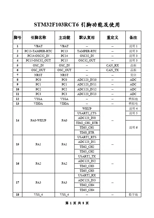
Excel格式的STM32F103引脚表
- 格式:xlsx
- 大小:18.78 KB
- 文档页数:16
2. FT = 5 V tolerant.
3. Function availability depends on the chosen device. For devices having reduced peripheral counts, it is always the lower nu
4. If several peripherals share the same I/O pin, to avoid conflict between these alternate functions only one peripheral should
5. PC13, PC14 and PC15 are supplied through the power switch. Since the switch only sinks a limited amount of current (3
6. Main function after the first backup domain power-up. Later on, it depends on the contents of the Backup registers even aft
7. Unlike in the LQFP64 package, there is no PC3 in the TFBGA64 package. The V REF+ functionality is provided instead.
8. This alternate function can be remapped by software to some other port pins (if available on the used package). For more de
9. The pins number 2 and 3 in the VFQFPN36 package, 5 and 6 in the LQFP48 and LQFP64 packages, and C1 and C2 in th The use of PD0 and PD1 in output mode is limited as they can only be used at 50 MHz in output mode.
wer number of peripheral that is included. For example, if a device has only one SPI and two USARTs, they will be called SPI1 and USART1 & US hould be enabled at a time through the peripheral clock enable bit (in the corresponding RCC peripheral clock enable register).
nt (3 mA), the use of GPIOs PC13 to PC15 in output mode is limited: the speed should not exceed 2 MHz with a maximum load of 30 pF and the en after reset (because these registers are not reset by the main reset). For details on how to manage these IOs, refer to the Battery backup dom
ore details, refer to the Alternate function I/O and debug configuration section in the STM32F10xxx reference manual, available from the STMicroe 2 in the TFBGA64 package are configured as OSC_IN/OSC_OUT after reset, however the functionality of PD0 and PD1 can be remapped by so
& USART2, respectively. Refer to Table 2 on page 10.
nd these IOs must not be used as a current source (e.g. to drive an LED).
domain and BKP register description sections in the STM32F10xxx reference manual, available from the STMicroelectronics website:
Microelectronics website: .
by software on these pins. For the LQFP100 package, PD0 and PD1 are available by default, so there is no need for remapping. For more details, r
.com.
ails, refer to the Alternate function I/O and debug configuration section in the STM32F10xxx reference manual.。