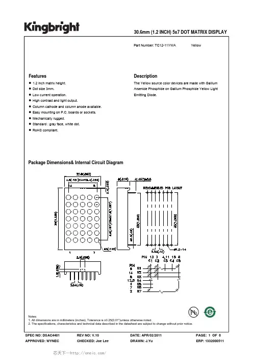
IXGH12N60CD1;中文规格书,Datasheet资料
- 格式:pdf
- 大小:82.68 KB
- 文档页数:3
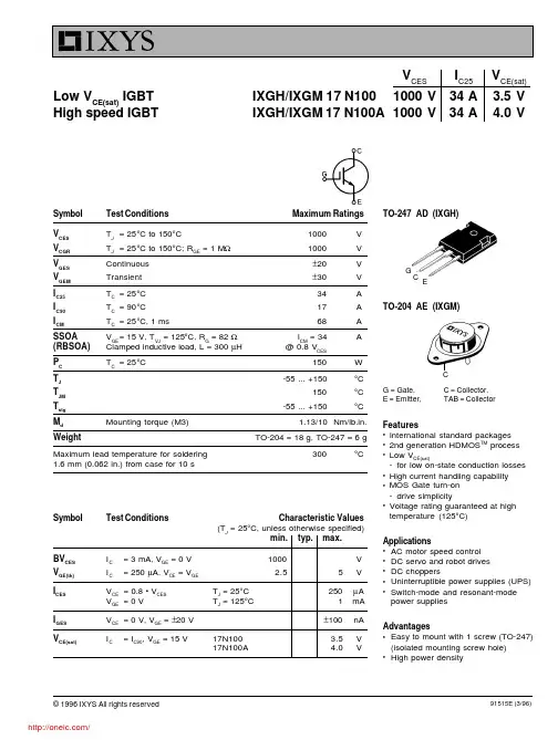
© 1996 IXYS All rights reservedSymbol Test Conditions Maximum RatingsV CES T J = 25°C to 150°C1000V V CGR T J = 25°C to 150°C; R GE = 1 M Ω1000V V GES Continuous ±20V V GEM Transient ±30V I C25T C = 25°C 34A I C90T C = 90°C 17A I CMT C = 25°C, 1 ms68A SSOA V GE = 15 V, T VJ = 125°C, R G = 82 Ω I CM = 34A (RBSOA)Clamped inductive load, L = 300 µH @ 0.8 V CESP C T C = 25°C150W T J -55 ... +150°C T JM 150°C T stg -55 ... +150°CM d Mounting torque (M3) 1.13/10Nm/lb.in.WeightTO-204 = 18 g, TO-247 = 6 gMaximum lead temperature for soldering 300°C1.6 mm (0.062 in.) from case for 10 sSymbol Test ConditionsCharacteristic Values(T J = 25°C, unless otherwise specified)min.typ.max.BV CES I C = 3 mA, V GE = 0 V 1000V V GE(th)I C= 250 µA, V CE = V GE2.55V I CES V CE = 0.8 • V CES T J = 25°C 250µA V GE = 0 VTJ = 125°C1mA I GES V CE = 0 V, V GE = ±20 V ±100nA V CE(sat)I C= I C90, V GE = 15 V17N100 3.5V 17N100A4.0VTO-247 AD (IXGH)V CESI C25V CE(sat)Low V CE(sat) IGBT IXGH/IXGM 17 N1001000 V 34 A 3.5 V High speed IGBTIXGH/IXGM 17 N100A 1000 V 34 A4.0 VGCETO-204 AE (IXGM)CG = Gate, C = Collector,E = Emitter,TAB = CollectorFeaturesl International standard packages l 2nd generation HDMOS TM process l Low V CE(sat)-for low on-state conduction losses l High current handling capability l MOS Gate turn-on -drive simplicitylVoltage rating guaranteed at high temperature (125°C)Applicationsl AC motor speed control l DC servo and robot drives l DC choppersl Uninterruptible power supplies (UPS)lSwitch-mode and resonant-mode power suppliesAdvantageslEasy to mount with 1 screw (TO-247)(isolated mounting screw hole)lHigh power density91515E (3/96)IXYS MOSFETS and IGBTs are covered by one or more of the following U.S. patents:4,835,5924,881,1065,017,5085,049,9615,187,1175,486,7154,850,0724,931,8445,034,7965,063,3075,237,4815,381,025IXYS reserves the right to change limits, test conditions, and dimensions.SymbolTest ConditionsCharacteristic Values(TJ = 25°C, unless otherwise specified)min.typ.max.g fs I C = I C90; V CE = 10 V,615S Pulse test, t ≤ 300 µs, duty cycle ≤ 2 %C ies 1500pF C oes V CE = 25 V, V GE = 0 V, f = 1 MHz175pF C res 40pF Q g 100120nC Q ge I C = I C90, V GE = 15 V, V CE = 0.5 V CES 2030nC Q gc 6090nC t d(on)100ns t ri 200ns t d(off)5001000ns t fi 17N100750ns 17N100A 450750ns E off 17N100A3mJ t d(on)100ns t ri 200ns E on 2.5mJ t d(off)7001000ns t fi 17N10012002000ns 17N100A 7501000ns E off 17N1008mJ 17N100A 6mJR thJC 0.83K/WR thCK0.25K/WIXGH 17N100 and IXGH 17N100 A characteristic curves are located on the IXGH 17N100U1 and IXGH 17N100AU1 data sheets.Inductive load, T J = 25°C I C = I C90, V GE = 15 V, L = 300 µH,V CE = 0.8 V CES , R G = R off = 82 ΩRemarks: Switching times may increasefor V CE (Clamp) > 0.8 • V CES ,higher T J or increased R G Inductive load, T J = 125°C I C = I C90, V GE = 15 V, L = 300 µH V CE = 0.8 V CES , R G = R off = 82 ΩRemarks: Switching times may increasefor V CE (Clamp) > 0.8 • V CES ,higher T J or increased R G分销商库存信息:IXYSIXGH17N100A IXGH17N100。
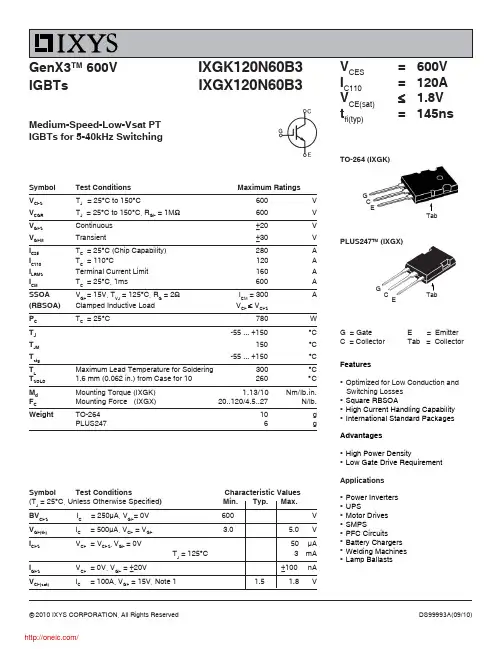
© 2010 IXYS CORPORATION, All Rights Reserved GenX3TM 600V IGBTsDS99993A(09/10)V CES = 600V I C110= 120A V CE(sat)≤ 1.8V t fi(typ)= 145nsMedium-Speed-Low-Vsat PT IGBTs for 5-40kHz SwitchingIXGK120N60B3IXGX120N60B3Symbol Test Conditions Characteristic Values (T J = 25°C, Unless Otherwise Specified ) Min. Typ. Max.BV CES I C = 250μA, V GE = 0V 600 VV GE(th)I C= 500μA, V CE = V GE3.05.0VI CES V CE = V CES , V GE = 0V50μA T J = 125°C 3 mA I GES V CE = 0V, V GE = ±20V ±100 nAV CE(sat)I C= 100A, V GE = 15V, Note 1 1.5 1.8 VSymbol Test Conditions Maximum RatingsV CES T J = 25°C to 150°C600 V V CGR T J = 25°C to 150°C, R GE = 1M Ω600 V V GES Continuous ±20 V V GEM Transient±30 VI C25T C = 25°C (Chip Capability)280 A I C110T C = 110°C 120 A I LRMS Terminal Current Limit 160 A I CMT C = 25°C, 1ms 600 A SSOA V GE = 15V, T VJ = 125°C, R G = 2Ω I CM = 300 A (RBSOA)Clamped Inductive Load V CE ≤ V CESP C T C = 25°C780 WT J -55 ... +150 °C T JM 150 °C T stg -55 ... +150 °CT LMaximum Lead Temperature for Soldering 300 °C T SOLD 1.6 mm (0.062 in.) from Case for 10 260 °C M d Mounting Torque(IXGK) 1.13/10 Nm/lb.in.F C Mounting Force (IXGX)20..120/4.5..27 N/lb.WeightTO-26410 g PLUS2476 gFeatureszOptimized for Low Conduction and Switching Losses zSquare RBSOA zHigh Current Handling Capability zInternational Standard PackagesAdvantagesz High Power DensityzLow Gate Drive RequirementApplicationsz Power Inverters z UPSz Motor Drives z SMPSz PFC Circuits z Battery Chargers z Welding Machines zLamp BallastsG = GateE = Emitter C = Collector Tab = CollectorTabTO-264 (IXGK)EC Tab6,727,5857,005,734 B2 7,157,338B2by one or moreof the following U.S. patents:4,850,0725,017,5085,063,3075,381,0256,259,123 B16,534,3436,710,405 B26,759,6927,063,975 B24,881,1065,034,7965,187,1175,486,7156,306,728 B16,583,5056,710,4636,771,478 B27,071,537Dim.Millimeter InchesMin.Max.Min.Max.A 4.82 5.13.190.202A1 2.54 2.89.100.114A2 2.00 2.10.079.083b 1.12 1.42.044.056b1 2.39 2.69.094.106b2 2.90 3.09.114.122c 0.530.83.021.033D 25.9126.16 1.020 1.030E 19.8119.96.780.786e 5.46 BSC .215 BSC J 0.000.25.000.010K 0.000.25.000.010L 20.3220.83.800.820L1 2.29 2.59.090.102P 3.17 3.66.125.144Q 6.07 6.27.239.247Q18.388.69.330.342R 3.81 4.32.150.170R1 1.78 2.29.070.090S 6.04 6.30.238.248T 1.57 1.83.062.072Terminals:1 - Gate2 - Collector3 - EmitterPLUS247TM (IXGX) Outlinelimeter Inches Min.Max.Min.Max.A 4.83 5.21.190.205A 1 2.29 2.54.090.100A 2 1.91 2.16.075.085b 1.14 1.40.045.055b 1 1.91 2.13.075.084b 2 2.923.12.115.123C 0.610.80.024.031D 20.8021.34.819.840E 15.7516.13.620.635e 5.45 BSC .215 BSC L 19.8120.32.780.800L1 3.81 4.32.150.170Q 5.59 6.20.2200.244R4.32 4.83.170.190Terminals: 1 = Gate2,4 = Collector3 = EmitterBack SideIXYS Reserves the Right to Change Limits, Test Conditions, and Dimensions.IXYS Reserves the Right to Change Limits, Test Conditions, and Dimensions.分销商库存信息: IXYSIXGX120N60B3。
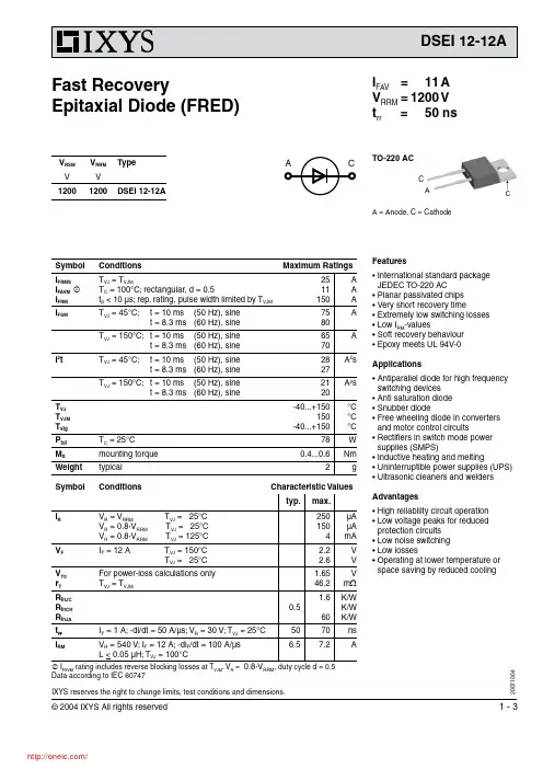
007 004IXYS reserves the right to change limits, test conditions and dimensions.Symbol Conditions Characteristic Valuestyp.max.I RV R = V RRM T VJ = 25°CV R = 0.8·V RRM T VJ = 25°C V R = 0.8·V RRM T VJ = 25°C 250 504µA µA mA V F I F = 2 A T VJ = 50°CT VJ = 25°C2.22.6V V V T0r T For power-loss calculations only T VJ = T VJM.6546.2V m W R thJC R thCH R thJA 0.5.660K/W K/W K/W t rr I F = A; -di/dt = 50 A/µs; V R = 30 V; T VJ = 25°C 5070ns I RMV R = 540 V; I F = 2 A; -di F /dt = 00 A/µs L < 0.05 µH; T VJ = 00°C6.57.2AI FAVM rating includes reverse blocking losses at T VJM . V R = 0.8·V RRM , duty cycle d = 0.5Data according to IEC 60747I FAV = 11 A V RRM = 1200 V t rr = 50 n sFast RecoveryEpitaxial Diode (FRED)Features• International standard package JEDEC TO-220 AC• Planar passivated chips • Very short recovery time• Extremely low switching losses • Low I RM -values• Soft recovery behaviour • Epoxy meets UL 94V-0Applications• Antiparallel diode for high frequency switching devices • Anti saturation diode • Snubber diode• Free wheeling diode in converters and motor control circuits• Rectifiers in switch mode power supplies (SMPS)• Inductive heating and melting• Uninterruptible power supplies (UPS)• Ultrasonic cleaners and welders Advantages• High reliability circuit operation • Low voltage peaks for reduced protection circuits • Low noise switching • Low losses• Operating at lower temperature or space saving by reduced coolingSymbol ConditionsMaximum RatingsI FRMS I FAVM I FRM T VJ = T VJMT C = 00°C; rectangular, d = 0.5t p < 0 µs; rep. rating, pulse width limited by T VJM 25 50A A A I FSMT VJ = 45°C; t = 0 ms (50 Hz), sinet = 8.3 ms (60 Hz), sine7580A T VJ = 50°C; t = 0 ms (50 Hz), sine t = 8.3 ms (60 Hz), sine6570A I 2tT VJ = 45°C; t = 0 ms (50 Hz), sinet = 8.3 ms (60 Hz), sine2827A 2s T VJ = 50°C; t = 0 ms (50 Hz), sine t = 8.3 ms (60 Hz), sine2 20A 2s T VJT VJM T stg -40...+ 5050-40...+ 50°C °C °C P tot T C = 25°C 78W M d mounting torque 0.4...0.6Nm Weight typical 2gA CTO-220 A CA = Anode, C = CathodeCC AV RSM V V RRM V Type12001200DSEI 12-12A007 004IXYS reserves the right to change limits, test conditions and dimensions.10030002004000.00.20.40.60.81.00.0010.010.11100.00.40.81.21.62.0040801201600.20.40.60.81.01.21.4K fT VJ [°C]-di F /dt [A/µs]t [s]100200300400102030405060020040060080010001200VF R [V ]di F/dt [A/µs]100300020040051525010203011010010000.00.51.01.52.02.53.00123102030I R M [A ]Q r [µC ]I F [A ]V F [V]-di F /dt [A/µs]t r r [n s ]t fr [µs]Z t h J C [k /W ]-di F /dt [A/µs]Q rI RMFig. Forward current versus voltage dropFig. 2 Recovery chargeversus -di F /dtFig. 3 Peak reverse current versus -di F /dtFig. 4 Dynamic parameters versus junction temperatureFig. 5 Recovery time versus -di F /dtFig. 7 T ransient thermal resistance junction to caseFig. 6 Peak forward voltageversus di F /dt007 004IXYS reserves the right to change limits, test conditions and dimensions.Dimensions TO-220 AC分销商库存信息: IXYSDSEI12-12A。
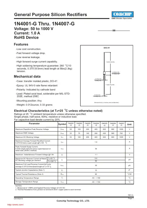
OElectrical Characteristics (at T A =25 C unless otherwise noted)ORatings at 25 C ambient temperature unless otherwise specified.Single phase, half wave, 60Hz, resistive or inductive load.For capacitive load derate current by 20%.ParameterSymbol UnitMaximum Repetitive Peak Reverse Voltage Maximum RMS Voltage Maximum DC Blocking VoltageMaximum Average Forward Rectified Current O 0.375"(9.5mm) Lead Length @T A =55C Peak Forward Surge Current, 8.3mS single half sine-wave superimposed on rated load (JEDEC method)Maximum Instantaneous Forward Voltage @1.0A Maximum DC Reverse Current at RatedOperating Temperature Range Storage Ttemperature RangeO T A =25C DC Blocking voltage per element Typical Junction Capacitance (Note 1)Typical Thermal Resistance (Note 2)503550V RRM V RMS V DC I (AV)I FSM V F I R C J R θJA T J T STG1.0305.0501560-55 ~ +150-55 ~ +150V V V AA V P FOC OCμA OC/WNOTES:1. Measured at 1.0MHz and Applied Reverse Voltage of 4.0V DC.22. Thermal Resistance from junction to terminal 6.0mm copper pads to each terminal.Voltage: 50 to 1000 V Current: 1.0 A RoHS DeviceFeatures-Low cost construction. -Fast forward voltage drop. -Low reverse leakage.-High forward surge current capability.O -High soldering temperature guarantee: 260C/10 seconds, 0.375”(9.5mm) lead length at 5lbs(2.3kg) tension.Mechanical data-Case: transfer molded plastic, DO-41 -Epoxy: UL 94V-0 rate flame retardant -Polarity: Indicated by cathode band-Lead: Plated axial lead, solderable per MIL-STD-202E, method 208C -Mounting position: Any-Weight: 0.012ounce, 0.33 grams10070100200140200400280400600420600800560800100070010001N4001-G Thru. 1N4007-G1.130-G 4001 1N -G 4002 1N -G 4003 1N -G 4004 1N -G 40051N -G 4006 1N -G 4007 1N O T A =100C Maximum Full Load Reverse Current,full cycle average 0.375”(9.5mm)lead length at T L =75 C O I R(AV)μARating and Characteristic Curves ( 1N4001) -G Thru. 4007-G1N Fig.2 Maximum. Non-Repetitive PeakForward Surge Current0ΙF S M , P e a k F o r w a r d S u r g e C u r r e n t (A )Number of Cycles at 60Hz1Fig.1 Typical Forward CurrentDerating CurveI (A V ), A v e r a g e F o r w a r d C u r r e n t (A )OT A , Ambient Temperature (C)02575175Fig.3 Typical Instantaneous ForwardCharacteristics0.01I F , I n s t a n t a n e o u s F o r w a r d C u r r e n t (A )V F , Instantaneous Forward Voltage (V)1.00.61.01.400.61.01.62.010015351.20.1Fig.4 Typical Reverse Characteristics0.01I R , I n s t a n t a n e o u s R e v e r s e C u r r e n t (m A )Percent of Peak Reverse Voltage (%)1.0100.11001250.40.80.81.8Fig.5 Typical Junction Capacitance10C J , C a p a c i t a n c e (p F )V R , Reverse Voltage (V)1000.11010010501500.21051025301.24080100140201206012010205025分销商库存信息: COMCHIP1N4002-G。

© 2002 IXYS All rights reserved98564A (06/02)Symbol Test Conditions Maximum RatingsVCES TJ= 25°C to 150°C600VVCGR TJ= 25°C to 150°C; RGE= 1 MΩ600VVGESContinuous±20VVGEMTransient±30VI C25TC= 25°C 14AI C90TC= 90°C 7AI CM TC= 25°C, 1 ms 30ASSOA VGE = 15 V, TVJ= 125°C, RG= 22 Ω ICM= 14A(RBSOA)Clamped inductive load, L = 300 µH @ 0.8 VCESPC TC= 25°C 54WTJ-55 (150)TJM150CTstg-55 (150)Maximum lead temperature for soldering 300C 1.6 mm (0.062 in.) from case for 10 sMd Mounting torque, (TO-220) M3 0.45/4 Nm/lb.in.M3.5 0.55/5 Nm/lb.in.Weight TO-220 4g TO-263 2 g Symbol Test Conditions Characteristic Values(TJ = 25°C, unless otherwise specified)min.typ.max.BVCESIC= 250 µA, VGE= 0 V600VVGE(th)IC= 250 µA, VCE= VGE2.5 5.5VI CES VCE= 0.8 • VCESTJ= 25°C100µA VGE= 0 V TJ= 125°C500µAI GES VCE= 0 V, VGE= ±20 V±100nAVCE(sat)IC= IC90, VGE= 15 V 2.0 2.7VFeatures•International standard packagesJEDEC TO-263 surfacemountable and JEDEC TO-220 AB•High frequency IGBT•High current handling capability•HiPerFAST TM HDMOS TM process•MOS Gate turn-on-drive simplicityApplications•Uninterruptible power supplies (UPS)•Switched-mode and resonant-modepower supplies•AC motor speed control•DC servo and robot drives•DC choppersAdvantages•High power density•Suitable for surface mounting•Very low switching losses for highfrequency applicationsVCES=600VIC25=14AVCE(sat)= 2.7Vtfi=45nsG = Gate, C = Collector,E = Emitter,TAB = CollectorHiPerFAST TM IGBT Lightspeed TM Series IXGA 7N60CIXGP 7N60CGEC (TAB)TO-263 AA (IXGA)TO-220AB (IXGP)IXYS reserves the right to change limits, test conditions, and dimensions.IXYS MOSFETs and IGBTs are covered by one or more of the following U.S. patents:4,835,5924,881,1065,017,5085,049,9615,187,1175,486,7156,306,728B14,850,0724,931,8445,034,7965,063,3075,237,4815,381,025SymbolTest ConditionsCharacteristic ValuesTO-220 AB Outlinelimeter Inches Min.Max.Min.Max.A 12.7013.970.5000.550B 14.7316.000.5800.630C9.9110.660.3900.420D 3.54 4.080.1390.161E 5.85 6.850.2300.270F 2.54 3.180.1000.125G 1.15 1.650.0450.065H 2.79 5.840.1100.230J 0.64 1.010.0250.040K 2.54BSC 0.100BSC M 4.32 4.820.1700.190N 1.14 1.390.0450.055Q 0.350.560.0140.022R2.29 2.790.0900.110TO-263 AA OutlinePins:1 - Gate2 - Collector3 - Emitter4 - CollectorBottom SideMin. Recommended Footprint (Dimensions in inches and mm)分销商库存信息:IXYSIXGP7N60C IXGA7N60C。
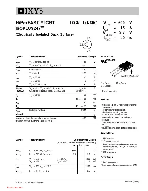
© 2002 IXYS All rights reservedSymbol Test Conditions Maximum RatingsV CES T J = 25°C to 150°C600V V CGR T J = 25°C to 150°C; R GE = 1 M Ω600V V GES Continuous ±20V V GEM Transient ±30V I C25T C = 25°C 15A I C90T C = 90°C 8A I CMT C = 25°C, 1 ms48A SSOAV GE = 15 V, T VJ = 125°C, R G = 33 Ω I CM = 24A(RBSOA)Clamped inductive load, L = 300 µH @ 0.8 V CESP C T C = 25°C55W T J -40 ... +150°C T JM 150°CT stg -40 ... +150°C V ISOL Isolation Voltage 2500V Weight5g Maximum lead temperature for soldering 300°C1.6 mm (0.062 in.) from case for 10 s98663B (02/02)Symbol Test ConditionsCharacteristic Values(T J = 25°C, unless otherwise specified)min.typ.max.BV CES I C = 250 µA, V GE = 0 V 600V V GE(th)I C= 250 µA, V GE = V GE2.55.0V I CES V CE = 0.8 V CES T J = 25°C 200µA V GE = 0 VT J = 125°C1.5mA I GES V CE = 0 V, V GE =±20 V ±100nA V CE(sat)I C= I T , V GE = 15 V2.7VV CES =600 VI C25=15A V CE(sat)= 2.7 Vt fi(typ)=55ns HiPerFAST TM IGBTISOPLUS247TM(Electrically Isolated Back Surface)G = Gate C = DrainE = Source* Patent pendingFeatureslSilicon chip on Direct-Copper-Bond substrate- High power dissipation - Isolated mounting surface - 2500V electrical isolationlLow collector to tab capacitance (<35pF)l 3rd generation HDMOS TM process V CE (sat)lRugged polysilicon gate cell structureApplicationslPFC circuitsl AC motor controllSwitched-mode and resonant-mode power supplies, UPS, no screws, or isolation foils lDC choppersAdvantagesl Easy assemblylLow capacitance to ground, low EMIIXGR 12N60CISOPLUS 247E153432Isolated Backside*IXYS reserves the right to change limits, test conditions, and dimensions.IXYS MOSFETS and IGBTs are covered by one or more of the following U.S. patents:4,835,5924,881,1065,017,5085,049,9615,187,1175,486,7156,306,728B14,850,0724,931,8445,034,7965,063,3075,237,4815,381,025SymbolTest ConditionsCharacteristic Values(T= 25°C, unless otherwise specified)Note: I T = 12A分销商库存信息: IXYSIXGR12N60C。
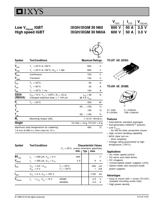
© 1996 IXYS All rights reservedTO-247 AD (IXGH)V CESI C25V CE(sat)Low V CE(sat) IGBT IXGH/IXGM 30 N60600 V 50 A 2.5 V High speed IGBTIXGH/IXGM 30 N60A600 V50 A3.0 VGCESymbol Test Conditions Maximum RatingsV CES T J = 25°C to 150°C600V V CGR T J = 25°C to 150°C; R GE = 1 M Ω600V V GES Continuous ±20V V GEM Transient ±30V I C25T C = 25°C 50A I C90T C = 90°C 30A I CMT C = 25°C, 1 ms100A SSOA V GE = 15 V, T VJ = 125°C, R G = 33 Ω I CM = 60A (RBSOA)Clamped inductive load, L = 100 µH @ 0.8 V CESP C T C = 25°C200W T J -55 ... +150°C T JM 150°C T stg -55 ... +150°CM d Mounting torque (M3) 1.13/10Nm/lb.in.WeightTO-204 = 18 g, TO-247 = 6gMaximum lead temperature for soldering 300°C1.6 mm (0.062 in.) from case for 10 sSymbol Test ConditionsCharacteristic Values(T J= 25°C, unless otherwise specified)min.typ.max.BV CES I C = 250 µA, V GE = 0 V 600V V GE(th)I C= 250 µA, V CE = V GE2.55V I CES V CE = 0.8 • V CES T J = 25°C 200µA V GE = 0 VT J= 125°C1mA I GES V CE = 0 V, V GE = ±20 V ±100nA V CE(sat)I C= I C90, V GE = 15 V30N60 2.5V 30N60A3.0VTO-204 AE (IXGM)CG = Gate, C = Collector,E = Emitter,TAB = CollectorFeaturesl International standard packages l 2nd generation HDMOS TM process l Low V CE(sat)-for low on-state conduction losses l High current handling capability l MOS Gate turn-on -drive simplicitylVoltage rating guaranteed at high temperature (125°C)Applicationsl AC motor speed control l DC servo and robot drives l DC choppersl Uninterruptible power supplies (UPS)lSwitch-mode and resonant-mode power suppliesAdvantageslEasy to mount with 1 screw (TO-247)(isolated mounting screw hole)lHigh power density91512E (3/96)IXYS MOSFETS and IGBTs are covered by one or more of the following U.S. patents:4,835,5924,881,1065,017,5085,049,9615,187,1175,486,7154,850,0724,931,8445,034,7965,063,3075,237,4815,381,025IXYS reserves the right to change limits, test conditions, and dimensions.SymbolTest ConditionsCharacteristic Values(T J = 25°C, unless otherwise specified)min.typ.max.g fs I C = I C90; V CE = 10 V,816S Pulse test, t ≤ 300 µs, duty cycle ≤ 2 %C ies 2800pF C oes V CE = 25 V, V GE = 0 V, f = 1 MHz230pF C res 70pF Q g 150180nC Q ge I C = I C90, V GE = 15 V, V CE = 0.5 V CES 3550nC Q gc 6090nC t d(on)100ns t ri 200ns t d(off)500ns t fi 30N60A 200ns E off 30N60A 2mJ t d(on)100ns t ri 200ns E on 3mJ t d(off)6001000ns t fi 30N605001500ns 30N60A250800ns E off 30N605.5mJ 30N60A 4.0mJ R thJC 0.62K/WR thCK0.25K/WIXGH 30N60 and IXGH 30N60A characteristic curves are located on theIXGH 30N60U1 and IXGH 30N60AU1 data sheets.Inductive load, T J = 25°CI C = I C90, V GE = 15 V, L = 300 µH V CE = 0.8 V CES , R G = R off = 33 ΩSwitching times may increasefor V CE (Clamp) > 0.8 • V CES ,higher T J or increased R GInductive load, T J = 125°C I C = I C90, V GE = 15 V,L = 300 µH V CE = 0.8 V CES ,R G = R off = 33 ΩRemarks: Switching timesmay increase for V CE(Clamp) > 0.8 • V CES , higher T J or increased R G。
1/9October 2003STGP12NB60HDN-CHANNEL 18A -600V TO-220PowerMESH™IGBTs HIGH INPUT IMPEDANCEs LOW ON-VOLTAGE DROP (V cesat )s OFF LOSSES INCLUDE TAIL CURRENT s LOW GATE CHARGEs HIGH CURRENT CAPABILITYs VERY HIGH FREQUENCY OPERATION sCO-PACKAGED WITH TURBOSWITCHT ANTIPARALLEL DIODEDESCRIPTIONUsing the latest high voltage technology based on a patented strip layout,STMicroelectronics has de-signed an advanced family ofIGBTs,the Power-MESH™IGBTs,with outstanding perfomances.The suffix "H"identifies a family optimized for high frequency applications (up to 50kHz)in order to achieve very high switching performances (reduced tfall)mantaining a lowvoltage drop.APPLICATIONSs HIGH FREQUENCY MOTOR CONTROLSs SMPS and PFC IN BOTH HARD SWITCH AND RESONANT TOPOLOGIES s UPSORDERING INFORMATIONTYPE V CES V CE(sat)(Max)@25°CI C@100°CSTGP12NB60HD600V<2.8 V 18ASALES TYPE MARKING PACKAGE PACKAGINGSTGP12NB60HDGP12NB60HDTO-220TUBEl s Ob so e t ePr od u c t () -l s l u )Ob so e t ePr od u c t () -O bs o e t eP r od c t(sSTGP12NB60HD2/9ABSOLUTE MAXIMUM RATINGS( )Pulse width limited by safe operating areaTHERMAL DATAELECTRICAL CHARACTERISTICS (T CASE =25°C UNLESS OTHERWISE SPECIFIED)OFFON (1)DYNAMICSymbol ParameterValue Unit V CES Collector-Emitter Voltage (V GS =0)600V V ECR Emitter-Collector Voltage 20V V GE Gate-Emitter Voltage±20V I C Collector Current (continuous)at T C =25°C (#)30A I C Collector Current (continuous)at T C =100°C (#)18A I CM ( )Collector Current (pulsed)60A P TOT Total Dissipation at T C =25°C 125W Derating Factor 1.0W/°C T stg Storage Temperature–65to 150°C T jMax.Operating Junction Temperature150°CRthj-case Thermal Resistance Junction-case Max 1.0°C/W Rthj-ambThermal Resistance Junction-ambient Max62.5°C/WSymbol ParameterTest ConditionsMin.Typ.Max.Unit V BR(CES)Collector-Emitter Breakdown Voltage I C =250µA,V GE =0600V I CES Collector cut-off (V GE =0)V CE =Max Rating,T C =25°C 50µA V CE =Max Rating,T C =125°C100µA I GESGate-Emitter Leakage Current (V CE =0)V GE =±20V ,V CE =0±100nASymbol ParameterTest ConditionsMin.Typ.Max.Unit V GE(th)Gate Threshold VoltageV CE =V GE ,I C =250µA 35V V CE(sat)Collector-Emitter Saturation VoltageV GE =15V,I C =12A2.0 2.8V V GE =15V,I C =12A,Tj =125°C1.7VSymbol Parameter Test ConditionsMin.Typ.Max.Unit g fsForward Transconductance V CE =15V ,I C =12A10S C iesInput Capacitance V CE =25V,f =1MHz,V GE =0920pF C oes Output Capacitance 120pF C res Reverse Transfer Capacitance27pF Q g Q ge Q gc Total Gate Charge Gate-Emitter Charge Gate-Collector Charge V CE =480V,I C =12A,V GE =15V681030nCnC nC I CLLatching CurrentV clamp =480V , Tj =150°C R G =10Ω48Al t l c )Ob so e t ePr od u c (s ) -O bs o e t eP r od u t (s3/9STGP12NB60HDELECTRICAL CHARACTERISTICS (CONTINUED)SWITCHING ONSWITCHING OFFCOLLECTOR-EMITTER DIODENote: 1.Pulsed:Pulse duration =300µs,duty cycle 1.5%.2.Pulse width limited by max.junction temperature.(**)Losses include Also the Tail (Jedec Standardization)(#)Calculated according to the iterative formula:Symbol ParameterTest ConditionsMin.Typ.Max.Unit t d(on)t r Turn-on Delay Time Rise TimeV CC =480V,I C =12A R G =10Ω,V GE =15V 546ns ns (di/dt)on EonTurn-on Current Slope Turn-on Switching LossesV CC =480V,I C =12A R G =10Ω,V GE =15V,Tj =125°C700290A/µs µJSymbol ParameterTest ConditionsMin.Typ.Max.Unit t c Cross-over Time V cc =480V,I C =12A,R GE =10Ω,V GE =15V150ns t r (V off )Off Voltage Rise Time 27ns t d (off )Delay Time 91ns t f Fall Time100nsE off (**)Turn-off Switching Loss 0.21m J E ts Total Switching Loss 0.49m Jt c Cross-over Time V cc =480V,I C =12A,R GE =10Ω,V GE =15V Tj =125°C230ns t r (V off )Off Voltage Rise Time 76ns t d (off )Delay Time 95ns t f Fall Time200nsE off (**)Turn-off Switching Loss 0.45m J E tsTotal Switching Loss0.74m JSymbolParameterTest ConditionsMin.Typ.Max.Unit I f I fm Forward CurrentForward Current pulsed 1248A A V f Forward On-VoltageI f =6AI f =6A,Tj =125°C1.31.1 1.9V V t rr Q rr I rrmReverse Recovery Time Reverse Recovery Charge Reverse Recovery CurrentI f =6A ,V R =50V,Tj =125°C,di/dt =100A/µs802405.5ns nC AI C T C ()T JMAX T C–R THJ C –V CESAT MAX ()T C I C ,()×--------------------------------------------------------------------------------------=-O STGP12NB60HDO-O 5/9STGP12NB60HDNormalized Breakdown Voltage vs TemperatureTotal Switching Losses vs TemperatureGate Charge vs Gate-Emitter Voltage Total Switching Losses vs Collector Currentll c Ob so e t eP-O bs o e t eP r od u t (STGP12NB60HD6/9l)O b s oe t eP ro d7/9STGP12NB60HDFig.2:Test Circuit For Inductive Load SwitchingFig.1:Gate Charge test CircuitSTGP12NB60HD8/9l slc)O b s oe t eP ro du ct()-O bs oe t eP ro dut(s9/9STGP12NB60HDInformation furnished is believed to be accurate and reliable. However, STMicroelectronics assumes no responsibility for the consequences of use of such information nor for any infringement of patents or other rights of third parties which may result from its use. No license is granted by implication or otherwise under any patent or patent rights of STMicroelectronics. Specifications mentioned in this publication are subject to change without notice. This publication supersedes and replaces all information previously supplied. STMicroelectronics products are not authorized for use as critical components in life support devices or systems without express written approval of STMicroelectronics.© The ST logo is a registered trademark of STMicroelectronics© 2003 STMicroelectronics - Printed in Italy - All Rights ReservedSTMicroelectronics GROUP OF COMPANIESAustralia - Brazil - Canada - China - Finland - France - Germany - Hong Kong - India - Israel - Italy - Japan - Malaysia - Malta - MoroccoSingapore - Spain - Sweden - Switzerland - United Kingdom - United States.© 分销商库存信息: STMSTGP12NB60HD。
玉林万顺达电脑芯片级维修资料 2010-07-20整理玉林万顺达电脑芯片级维修资料 2010-07-20整理玉林万顺达电脑芯片级维修资料 2010-07-20整理玉林万顺达电脑芯片级维修资料 2010-07-20整理玉林万顺达电脑芯片级维修资料 2010-07-20整理玉林万顺达电脑芯片级维修资料 2010-07-20整理玉林万顺达电脑芯片级维修资料 2010-07-20整理玉林万顺达电脑芯片级维修资料 2010-07-20整理玉林万顺达电脑芯片级维修资料 2010-07-20整理玉林万顺达电脑芯片级维修资料 2010-07-20整理玉林万顺达电脑芯片级维修资料 2010-07-20整理玉林万顺达电脑芯片级维修资料 2010-07-20整理玉林万顺达电脑芯片级维修资料 2010-07-20整理玉林万顺达电脑芯片级维修资料 2010-07-20整理玉林万顺达电脑芯片级维修资料 2010-07-20整理玉林万顺达电脑芯片级维修资料 2010-07-20整理玉林万顺达电脑芯片级维修资料 2010-07-20整理玉林万顺达电脑芯片级维修资料 2010-07-20整理玉林万顺达电脑芯片级维修资料 2010-07-20整理玉林万顺达电脑芯片级维修资料 2010-07-20整理玉林万顺达电脑芯片级维修资料 2010-07-20整理玉林万顺达电脑芯片级维修资料 2010-07-20整理玉林万顺达电脑芯片级维修资料 2010-07-20整理玉林万顺达电脑芯片级维修资料 2010-07-20整理玉林万顺达电脑芯片级维修资料 2010-07-20整理玉林万顺达电脑芯片级维修资料 2010-07-20整理玉林万顺达电脑芯片级维修资料 2010-07-20整理玉林万顺达电脑芯片级维修资料 2010-07-20整理玉林万顺达电脑芯片级维修资料 2010-07-20整理玉林万顺达电脑芯片级维修资料 2010-07-20整理。