ADSP2191若干概念
- 格式:docx
- 大小:368.35 KB
- 文档页数:6

第4章用ADS仿真无线通信链路 (2)4.1 ADS简介以及特点 (2)4.2 软件基本操作 (3)4.2.1 软件界面 (3)4.2.2 用户界面 (3)4.2.3 基本操作 (5)4.3 发射链路 (20)4.3.1 模型参数 (20)4.3.2发射链路的设计 (22)4.3.3 AGC自动控制增益 (33)4.3.4链路参数扫描 (42)4.4 接收链路 (55)4.4.1 模型参数 (55)4.4.2 接收链路设计 (56)4.4.3 AGC自动控制增益 (65)4.4.4链路参数扫描 (69)4.5 发射和接收链路级联 (81)4.5.1链路设计 (81)4.5.2链路参数扫描 (84)4.6 总结 (97)第4章用ADS仿真无线通信链路4.1 ADS简介以及特点先进设计系统(Advanced Design System),简称ADS,是安捷伦科技有限公司(Agilent)为适应竞争形势,为了高效的进行产品研发生产,而设计开发的一款EDA软件。
软件迅速成为工业设计领域EDA软件的佼佼者,因其强大的功能、丰富的模板支持和高效准确的仿真能力(尤其在射频微波领域),而得到了广大IC设计工作者的支持。
ADS是高频设计的工业领袖。
它支持系统和射频设计师开发所有类型的射频设计,从简单到最复杂,从射频∕微波模块到用于通信和航空航天∕国防的MMIC。
ADS 的主要特点在于可以快速、精确、简单易用的全套集成系统、电路和电磁仿真器,能够一次性成功完成桌面流程设计。
而且特定应用设计指南将长期积累的专业知识应用于简单易用的界面中。
ADS电子设计自动化功能十分强大,包含时域电路仿真 (SPICE-like Simulation)、频域电路仿真 (Harmonic Balance、Linear Analysis)、三维电磁仿真 (EM Simulation)、通信系统仿真(Communication System Simulation)、数字信号处理仿真设计(DSP);ADS支持射频和系统设计工程师开发所有类型的RF设计,从简单到复杂,从离散的射频/微波模块到用于通信和航天/国防的集成MMIC,是当今国内各大学和研究所使用最多的微波/射频电路和通信系统仿真软件软件。
ADSP仿真作业专业:电磁场与微波技术学生成员:刘航(M201571827) 完成时间:2019年12月8日目录目录 (1)图目录 (2)1题目1 (3)1.1题目 (3)1.2算法模型 (3)1.2.1自适应滤波原理 (3)1.2.2LMS算法简介 (3)1.2.3LSL算法简介 (4)1.3本题模型 (5)1.4仿真过程及结果分析 (6)1.4.1仿真过程 (6)1.4.2结果分析 (8)2题目2 (9)2.1题目 (9)2.2算法模型 (9)2.2.1特征分解频率估计原理 (9)2.2.2Music算法简介 (10)2.2.3PHD算法简介 (10)2.3仿真过程及结果分析 (11)2.3.1仿真过程 (11)2.3.2结果分析 (13)3附录 (14)3.1题目1源程序 (14)3.2题目2源程序 (15)图目录图 1.1自适应滤波器框图 (3)图 1.2 题目一模型 (5)图 1.3 LSL和LMS算法估计信号模型参数的性能比较 (8)图 1.4 初始预测误差 对LSL收敛性能的影响 (9)图 2.1 MUSIC算法得到的谱峰 (13)1题目11.1 题目Implement LSL algorithm and LMS algorithm based on figure 3.30(P92) and figure 3.31(P93). Model and parameters see page 91.P91模型如下:二阶自回归随机过程x(n)=a1x(n-1)+a2x(n-2)+w(n),对应的滤波器参数a1=1.558,a2 =-0.81。
分别用LMS算法和LSL算法预测信号x(n),从而得到对信号模型的两个参数值的估计值。
1.2 算法模型1.2.1自适应滤波原理自适应滤波器由参数可调的数字滤波器和自适应算法两部分组成,其原理如下图所示:图1.1自适应滤波器框图输入信号x(n)通过参数可调的数字滤波器后产生输出信号y(n),将其与期望输出信号d(n)进行比较,形成误差信号e(n)。

基于ADSP21161的比相测距雷达跟踪控制系统设计摘要介绍了21161的结构及性能,主要讨论了其在连续波比相测距雷达中的应用。
介绍了比相测距雷达的基本原理,分析以为核心的雷达跟踪控制系统的硬件结构软件设计,详细讨论了软件部分的设计和实现。
测试结果表明,整套系统较好地满足了设计要求。
关键词21161连续波雷达比相测距连续波雷达具有测量精度高、设备简单等优点。
连续波比相测距雷达继承了连续波雷达的固有优点,由于采用了比相技术,不仅克服了一般连续波雷达测距困难的缺点,而且又便于利用现代信号处理的新技术。
随着近年来低截获概率雷达发展的需要,其研究日益受到人们的重视。
采用新的数字信号处理器件,不仅大大降低了雷达本身的设计复杂度,而且极大地提高了雷达的整体性能。
121161的主要特点21161是美国公司生产的一款高性能的32位浮点处理器。
在一个单独的芯片上集成了具有强大浮点运算能力的微处理器内核、1的零等待、多种形式的外部接口和独立的/控制器,构成了一个完整的系统;超级哈佛结构的和高速指令使得21161的指令均为单周期指令;6套独立的总线分别用于程序存储区和数据存储区,可以同时对和进行数据访问;经优化的和中断的传输机制使得其与外部的数据交换独立且并行于处理器内核的运算过程;片内的主机接口和总线仲裁器可以使多片处理器无需任何附加资源即可构成多处理器阵列。
该处理器适用于各种高性能的数字信号处理任务和构成多处理器阵列。
21161的主要特点包括1100的内核工作频率;600每秒百万次浮点运算的浮点运算峰值;单片21161完成1024点复数仅需92μ。
范文先生网收集整理232位单精度或40位扩展精度浮点处理器内核;有3个独立的关联计算单元分别为算术/逻辑单元、乘法器和移位器;完备的算术运算指令集;具有16个通用寄存器组;所有运算指令均为单周期指令;支持零等待循环执行和条件转移。
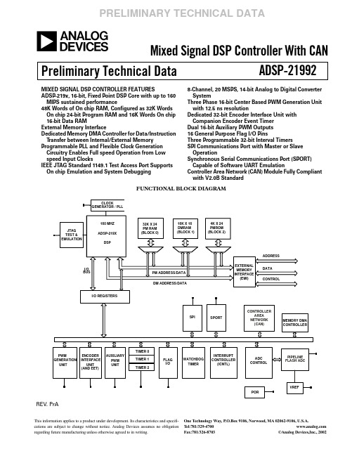
aPreliminary Technical DataMixed Signal DSP Controller With CANThis information applies to a product under development. Its characteristics and specifi-cations are subject to change without notice. Analog Devices assumes no obligation regarding future manufacturing unless otherwise agreed to in writing.One Technology Way, P.O.Box 9106, Norwood, MA 02062-9106, U.S.A.Tel:781/329-4700 Fax:781/326-8703 ©Analog Devices,Inc., 2002REV. PrA ADSP-21992MIXED SIGNAL DSP CONTROLLER FEATURESADSP-219x, 16-bit, Fixed Point DSP Core with up to 160 MIPS sustained performance48K Words of On chip RAM, Configured as 32K Words On chip 24-bit Program RAM and 16K Words On chip 16-bit Data RAMExternal Memory InterfaceDedicated Memory DMA Controller for Data/Instruction T ransfer between Internal/External Memory Programmable PLL and Flexible Clock Generation Circuitry Enables Full speed Operation from Low speed Input ClocksIEEE JTAG Standard 1149.1 T est Access Port Supports On chip Emulation and System Debugging 8-Channel, 20 MSPS, 14-bit Analog to Digital Converter SystemThree Phase 16-bit Center Based PWM Generation Unit with 12.5 ns resolutionDedicated 32-bit Encoder Interface Unit with Companion Encoder Event TimerDual 16-bit Auxiliary PWM Outputs16 General Purpose Flag I/O PinsThree Programmable 32-bit Interval TimersSPI Communications Port with Master or Slave OperationSynchronous Serial Communications Port (SPORT) Capable of Software UART EmulationController Area Network (CAN) Module Fully Compliant with V2.0B StandardFUNCTIONAL BLOCK DIAGRAMFor current information contact Analog Devices at (781) 937-1799ADSP-21992August 2002This information applies to a product under development. Its characteristics and specifications are subject to change without notice. Analog Devices assumes no obligation regarding future manufacturing unless otherwise agreed to in writing.2REV. PrAIntegrated Watchdog TimerDedicated Peripheral Interrupt Controller with Software Priority Control Multiple Boot ModesPrecision 1.0V Voltage ReferenceIntegrated Power-On-Reset (POR) GeneratorFlexible Power Management with Selectable Powerdown and Idle Modes2.5V Internal Operation with3.3V I/OOperating T emperature Range of –40ºC to +115ºC 176 pin LQFP packageT ARGET APPLICATIONS Industrial Motor DrivesUn-Interruptible Power Supplies Optical Networking Control Data Acquisition SystemsT est and Measurement Systems Portable Instrumentation GENERAL NOTEThis data sheet provides preliminary information for the ADSP-21992 Mixed Signal Digital Signal Processor.GENERAL DESCRIPTIONThe ADSP-21992 is a mixed signal DSP controller based on the ADSP-219x DSP Core, suitable for a variety of high performance Industrial Motor Control and Signal Process-ing applications that require the combination of a high performance DSP and the mixed signal integration of embedded control peripherals such as analog to digital con-version with communications interfaces such as CAN.The ADSP-21992 integrates the 160 MIPS, fixed point ADSP-219x family base architecture with a serial port, an SPI compatible port, a DMA controller, three programma-ble timers, general purpose Programmable Flag pins,extensive interrupt capabilities, on chip program and data memory spaces, and a complete set of embedded control peripherals that permits fast motor control and signal pro-cessing in a highly integrated environment.The ADSP-21992 architecture is code compatible with previous ADSP-217x based ADMCxxx products. Although the architectures are compatible, the ADSP-21992, with ADSP-219x architecture, has a number of enhancements over earlier architectures. The enhancements to computa-tional units, data address generators, and programsequencer make the ADSP-21992 more flexible and easier to program than the previous ADSP-21xx embedded DSPs.Indirect addressing options provide addressing flexibility—premodify with no update, pre- and post-modify by an immediate 8-bit, two’s complement value and base address registers for easier implementation of circular buffering.The ADSP-21992 integrates 48K words of on chip memory configured as 32K words (24-bit) of program RAM, and 16K words (16-bit) of data RAM.Fabricated in a high speed, low power, CMOS process, the ADSP-21992 operates with a 6.25ns instruction cycle time (160MIPS). All instructions, except two multiword instructions, execute in a single DSP cycle.The ADSP-21992’s flexible architecture and comprehen-sive instruction set support multiple operations in parallel. For example, in one processor cycle, the ADSP-21992 can:•Generate an address for the next instruction fetch •Fetch the next instruction •Perform one or two data moves•Update one or two data address pointers •Perform a computational operationThese operations take place while the processor continues to:•Receive and transmit data through the serial port •Receive or transmit data over the SPI port•Access external memory through the external memory interface•Decrement the timers•Operate the embedded control peripherals (ADC, PWM, EIU, etc.)DSP Core Architecture•6.25 ns instruction cycle time (internal), for up to 160 MIPS sustained performance•ADSP-218x family code compatible with the same easy to use algebraic syntax•Single cycle instruction execution•Up to 1 Mwords of addressable memory space with twenty four bits of addressing width•Dual purpose program memory for both instruction and data storage•Fully transparent Instruction Cache allows dual operand fetches in every instruction cycle•Unified memory space permits flexible address genera-tion, using two independent DAG units•Independent ALU, Multiplier/Accumulator, and barrel Shifter computational units with dual 40-bit accumulators•Single cycle context switch between two sets of computa-tional and DAG registers•Parallel execution of computation and memory instructions•Pipelined architecture supports efficient code execution at speeds up to 160 MIPS•Register file computations with all non-conditional, non-parallel computational instructions•Powerful Program Sequencer provides zero overhead looping and conditional instruction executionThis information applies to a product under development. Its characteristics and specifications are subject to change without notice. Analog Devices assumes no obligation regarding future manufacturing unless otherwise agreed to in writing.3REV. PrA For current information contact Analog Devices at (781) 937-1799ADSP-21992August 2002•Architectural enhancements for compiled C code efficiency•Architecture enhancements beyond ADSP-218x family are supported with instruction set extensions for added registers, ports, and peripherals.The clock generator module of the ADSP-21992 includes Clock Control logic that allows the user to select and change the main clock frequency. The module generates two output clocks; the DSP core clock, CCLK, and the peripheral clock, HCLK. CCLK can sustain clock values of up to 160 MHz, while HCLK can be equal to CCLK or CCLK/2 for values up to a maximum 80MHz peripheral clock.The ADSP-21992 instruction set provides flexible data moves and multifunction (one or two data moves with a computation) instructions. Every single word instruction can be executed in a single processor cycle. TheADSP-21992 assembly language uses an algebraic syntax for ease of coding and readability. A comprehensive set of development tools supports program development.The block diagram Figure1 shows the architecture of the embedded ADSP-219x core. It contains three independent computational units: the ALU, the multiplier/accumulator (MAC), and the shifter. The computational units process 16-bit data from the register file and have provisions to support multiprecision computations. The ALU performs a standard set of arithmetic and logic operations; division primitives are also supported. The MAC performs single cycle multiply, multiply/add, and multiply/subtract opera-tions. The MAC has two 40-bit accumulators, which help with overflow. The shifter performs logical and arithmetic shifts, normalization, denormalization, and derive exponent operations. The shifter can be used to efficiently implement numeric format control, including multiword and block floating point representations.Register usage rules influence placement of input and results within the computational units. For most operations, the computational units’ data registers act as a data register file, permitting any input or result register to provide input to any unit for a computation. For feedback operations, the computational units let the output (result) of any unit beFigure 1.ADSP-21992 DSP Block DiagramFor current information contact Analog Devices at (781) 937-1799ADSP-21992August 2002This information applies to a product under development. Its characteristics and specifications are subject to change without notice. Analog Devices assumes no obligation regarding future manufacturing unless otherwise agreed to in writing.4REV. PrAinput to any unit on the next cycle. For conditional or mul-tifunction instructions, there are restrictions on which data registers may provide inputs or receive results from each computational unit. For more information, see the ADSP-219x DSP Instruction Set Reference .A powerful program sequencer controls the flow of instruc-tion execution. The sequencer supports conditional jumps, subroutine calls, and low interrupt overhead. With internal loop counters and loop stacks, the ADSP-21992 executes looped code with zero overhead; no explicit jump instruc-tions are required to maintain loops.Two data address generators (DAGs) provide addresses for simultaneous dual operand fetches (from data memory and program memory). Each DAG maintains and updates four 16-bit address pointers. Whenever the pointer is used to access data (indirect addressing), it is pre- or post-modified by the value of one of four possible modify registers. A length value and base address may be associated with each pointer to implement automatic modulo addressing for circular buffers. Page registers in the DAGs allow circular addressing within 64K word boundaries of each of the 256 memory pages, but these buffers may not cross page boundaries. Secondary registers duplicate all the primary registers in the DAGs; switching between primary and secondary registers provides a fast context switch.Efficient data transfer in the core is achieved with the use of internal buses:•Program Memory Address (PMA) Bus •Program Memory Data (PMD) Bus •Data Memory Address (DMA) Bus •Data Memory Data (DMD) Bus •Direct Memory Access Address Bus •Direct Memory Access Data BusThe two address buses (PMA and DMA) share a single external address bus, allowing memory to be expanded off chip, and the two data buses (PMD and DMD) share a single external data bus. Boot memory space and I/O memory space also share the external buses.Program memory can store both instructions and data, per-mitting the ADSP-21992 to fetch two operands in a single cycle, one from program memory and one from data memory. The DSP’s dual memory buses also let the embedded ADSP-219x core fetch an operand from data memory and the next instruction from program memory in a single cycle.Memory ArchitectureThe ADSP-21992 provides 48K words of on chip SRAM memory. This memory is divided into two blocks; a 32K x 24-bit (block 0) and a 16K x 16-bit (block 1). In addition, the ADSP-21992 provides a 4k x 24-bit block of programmemory boot ROM (that is reserved by ADI for boot load routines). The memory map of the ADSP-21992 is illus-trated in Figure 2.As shown in Figure 2, the two internal memory RAM blocks reside in memory page 0. The entire DSP memory map consists of 256 pages (pages 0 to 255), and each page is 64 kWords long. External memory space consists of four memory banks (banks 0-3) and supports a wide variety of memory devices. Each bank is selectable using unique memory select lines (MS3 - MS0) and has configurable page boundaries, wait states, and wait state modes. The 4K words of on chip boot ROM populates the top of page 255, while the remaining 254 pages are addressable off chip. I/Omemory pages differ from external memory in that they are 1K word long, and the external I/O pages have their own select pin (IOMS). Pages 0-31 of I/O memory space reside on chip and contain the configuration registers for the peripherals. Both the ADSP_219x core and DMA capable peripherals can access the DSP’s entire memory map.NOTE: The physical external memory addresses are limited by 20 address lines, and are determined by the external data width and packing of the external memory space. The Strobe signals (MS3 - 0) can be programmed to allow the user to change starting page addresses at run time.Internal (On chip) MemoryThe ADSP-21992’s unified program and data memory space consists of 16M locations that are accessible through two 24-bit address buses, the PMA and DMA buses. TheFigure 2.ADSP-21992 DSP Core Memory Map at ResetThis information applies to a product under development. Its characteristics and specifications are subject to change without notice. Analog Devices assumes no obligation regarding future manufacturing unless otherwise agreed to in writing.5REV. PrA For current information contact Analog Devices at (781) 937-1799ADSP-21992August 2002DSP uses slightly different mechanisms to generate a 24-bit address for each bus. The DSP has three functions that support access to the full memory map.•The DAGs generate 24-bit addresses for data fetches from the entire DSP memory address range. Because DAG index (address) registers are 16 bits wide and hold the lower 16bits of the address, each of the DAGs has its own 8-bit page register (DMPGx) to hold the most significant eight address bits. Before a DAG generates an address, the program must set the DAG’s DMPGx register to the appropriate memory page. The DMPG1 register is also used as a page register when accessing external memory. The program must set DMPG1 accordingly, when accessing data variables in external memory. A 'C' program macro is provided for setting this register.•The Program Sequencer generates the addresses for instruction fetches. For relative addressing instructions, the program sequencer bases addresses for relative jumps, calls, and loops on the 24-bit Program Counter (PC). In direct addressing instructions (two word instructions), the instruction provides an immediate 24-bit address value. The PC allows linear addressing of the full 24-bit address range.•For indirect jumps and calls that use a 16-bit DAG address register for part of the branch address, the Program Sequencer relies on an 8-bit Indirect Jump page (IJPG) register to supply the most significant eight address bits. Before a cross page jump or call, the program must set the program sequencer’s IJPG register to the appropriate memory page.The ADSP-21992 has 4K word of on chip ROM that holds boot routines. The DSP starts executing instructions from the on chip boot ROM, which starts the boot process. For more information, see Booting Modes on page14. The on chip boot ROM is located on Page255 in the DSP’s memory space map, starting at address 0xFF0000. External (Off Chip) MemoryEach of the ADSP-21992’s off chip memory spaces has a separate control register, so applications can configure unique access parameters for each space. The access param-eters include read and write wait counts, wait state completion mode, I/O clock divide ratio, write hold time extension, strobe polarity, and data bus width. The core clock and peripheral clock ratios influence the external memory access strobe widths. For more information, see Clock Signals on page13. The off chip memory spaces are:•External memory space (MS3–0 pins)•I/O memory space (IOMS pin)•Boot memory space (BMS pin)All of these off chip memory spaces are accessible through the External Port, which can be configured for 8-bit or16-bit data widths.External Memory SpaceExternal memory space consists of four memory banks. These banks can contain a configurable number of 64 k Word pages. At reset, the page boundaries for external memory have Bank0 containing pages 1 to 63, Bank1 con-taining pages 64 to 127, Bank2 containing pages 128 to 191, and Bank3 containing pages 192 to 254. The MS3-MS0 memory bank pins select Banks 3-0, respectively. Both the ADSP-219x core and DMA capable peripherals can access the DSP’s external memory space.All accesses to external memory are managed by the External Memory Interface Unit (EMI).I/O Memory SpaceThe ADSP-21992 supports an additional external memory called I/O memory space. The IO space consists of 256 pages, each containing 1024 addresses. This space is designed to support simple connections to peripherals (such as data converters and external registers) or to bus interface ASIC data registers. The first 32K addresses (IO pages 0 to 31) are reserved for on chip peripherals. The upper 224k addresses (IO pages 32 to 255) are available for external peripheral devices. External I/O pages have their own select pin (IOMS). The DSP instruction set provides instructions for accessing I/O space.Boot Memory SpaceBoot memory space consists of one off chip bank with 254 pages. The BMS memory bank pin selects boot memory space. Both the ADSP-219x core and DMA capable periph-Figure 3.ADSP-21992 I/O Memory MapFor current information contact Analog Devices at (781) 937-1799ADSP-21992August 2002This information applies to a product under development. Its characteristics and specifications are subject to change without notice. Analog Devices assumes no obligation regarding future manufacturing unless otherwise agreed to in writing.6REV. PrAerals can access the DSP’s off chip boot memory space. After reset, the DSP always starts executing instructions from the on chip boot ROM.Bus Request and Bus GrantThe ADSP-21992 can relinquish control of the data and address buses to an external device. When the external device requires access to the bus, it asserts the bus request (BR) signal. The (BR) signal is arbitrated with core and peripheral requests. External Bus requests have the lowest priority. If no other internal request is pending, the external bus request will be granted. Due to synchronizer and arbi-tration delays, bus grants will be provided with a minimum of three peripheral clock delays. The ADSP-21992 will respond to the bus grant by:•Three stating the data and address buses and the MS3–0, BMS, IOMS, RD, and WR output drivers.•Asserting the bus grant (BG) signal.The ADSP-21992 will halt program execution if the bus is granted to an external device and an instruction fetch or data read/write request is made to external general purpose or peripheral memory spaces. If an instruction requires two external memory read accesses, the bus will not be granted between the two accesses. If an instruction requires an external memory read and an external memory write access, the bus may be granted between the two accesses. The external memory interface can be configured so that the core will have exclusive use of the interface. DMA and Bus Requests will be granted. When the external device releases BR, the DSP releases BG and continues program execution from the point at which it stopped.The bus request feature operates at all times, even while the DSP is booting and RESET is active.The ADSP-21992 asserts the BGH pin when it is ready to start another external port access, but is held off because the bus was previously granted. This mechanism can be extended to define more complex arbitration protocols for implementing more elaborate multimaster systems.DMA ControllerThe ADSP-21992 has a DMA controller that supports automated data transfers with minimal overhead for the DSP core. Cycle stealing DMA transfers can occur between the ADSP-21992’s internal memory and any of its DMA capable peripherals. Additionally, DMA transfers can be accomplished between any of the DMA capable peripherals and external devices connected to the external memory interface. DMA capable peripherals include the SPORT and SPI ports, and ADC Control module. Each individual DMA capable peripheral has a dedicated DMA channel. T o describe each DMA sequence, the DMA controller uses a set of parameters—called a DMA descriptor. When succes-sive DMA sequences are needed, these DMA descriptors can be linked or chained together, so the completion of one DMA sequence auto initiates and starts the next sequence. DMA sequences do not contend for bus access with the DSP core, instead DMAs “steal” cycles to access memory. All DMA transfers use the DMA bus shown in Figure 1 on page 3. Because all of the peripherals use the same bus, arbitration for DMA bus access is needed. The arbitration for DMA bus access appears in Table 1.DSP Peripherals ArchitectureThe ADSP-21992 contains a number of special purpose, embedded control peripherals, which can be seen in the Functional Block diagram on page 1. The ADSP-21992 contains a high performance, 8-channel, 14-bit ADC system with dual channel simultaneous sampling ability across 4 pairs of inputs. An internal precision voltage reference is also available as part of the ADC system. In addition, a three phase, 16-bit, center based PWM genera-tion unit can be used to produce high accuracy PWM signals with minimal processor overhead. The ADSP-21992 also contains a flexible incremental encoder interface unit for position sensor feedback; two adjustable frequency auxiliary PWM outputs, 16 lines of digital I/O; a 16-bit watchdog timer; three general purpose timers and an interrupt con-troller that manages all peripheral interrupts. Finally, the ADSP-21992 contains an integrated power-on-reset (POR) circuit that can be used to generate the required reset signal for the device on power-on.The ADSP-21992 has an external memory interface that is shared by the DSP’s core, the DMA controller, and DMA capable peripherals, which include the ADC, SPORT, and SPI communication ports. The external port consists of a 16-bit data bus, a 20-bit address bus, and control signals.Figure 4.ADSP-21992 Boot Memory Map T able 1. I/O Bus Arbitration Priority DMA Bus MasterArbitration PrioritySPORT Receive DMA 0—Highest SPORT Transmit DMA 1ADC Control DMA2SPI0 Receive/Transmit DMA 3Memory DMA4—LowestThis information applies to a product under development. Its characteristics and specifications are subject to change without notice. Analog Devices assumes no obligation regarding future manufacturing unless otherwise agreed to in writing.7REV. PrA For current information contact Analog Devices at (781) 937-1799ADSP-21992August 2002The data bus is configurable to provide an 8 or 16bit interface to external memory. Support for word packing lets the DSP access 16- or 24-bit words from external memory regardless of the external data bus width.The memory DMA controller lets the ADSP-21992 move data and instructions from between memory spaces: inter-nal-to-external, internal-to-internal, and external-to- external. On chip peripherals can also use this controller for DMA transfers.The embedded ADSP-219x core can respond to up to seventeen interrupts at any given time: three internal (stack, emulator kernel, and power down), two external (emulator and reset), and twelve user defined (peripherals) interrupts. Programmers assign each of the 32 peripheral interrupt requests to one of the 12 user defined interrupts. These assignments determine the priority of each peripheral for interrupt service.The following sections provide a functional overview of the ADSP-21992 peripherals.Serial Peripheral Interface (SPI) PortThe Serial Peripheral Interface (SPI) Port provides func-tionality for a generic configurable serial port interface based on the SPI standard, which enables the DSP to com-municate with multiple SPI compatible devices. Key features of the SPI port are:•Interface to host microcontroller or serial EEPROM •Master or slave operation (3 Wire Interface MISO, MOSI, SCK)•Data rates to 20 Mbaud (16-bit baud rate selector)•8 or 16-bit transfer•Programmable clock phase & polarity•Broadcast Mode - 1 master, multiple slaves•DMA capability & Dedicated interrupts•PF0 can be used as Slave Select Input Line•PF1-PF7 can be used as external Slave Select output SPI is a 3 wire interface consisting of 2 data pins (MOSI and MISO), one clock pin (SCK), and a single Slave Select input (SPISS0) that is multiplexed with the PF0 Flag IO line and seven Slave Select outputs (SPISEL1 to SPISEL7) that are multiplexed with the PF1 to PF7 Flag IO lines. The SPISS0 input is used to select the ADSP-21992 as a slave to an external master. The SPISEL1 to SPISEL7 outputs can be used by the ADSP-21992 (acting as a master) to select/enable up to seven external slaves in an multi device SPI configuration. In a multimaster or a multi device con-figuration, all MOSI pins are tied together, all MISO pins are tied together, and all SCK pins are tied together. During transfers, the SPI port simultaneously transmits and receives by serially shifting data in and out on the serial data line. The serial clock line synchronizes the shifting and sampling of data on the serial data line.In master mode, the DSP’s core performs the following sequence to set up and initiate SPI transfers:1.Enables and configures the SPI port operation (datasize, and transfer format).2.Selects the target SPI slave with the SPISELx outputpin (reconfigured Programmable Flag pin).3.Defines one or more DMA descriptors in Page0 of I/Omemory space (optional in DMA mode only).4.Enables the SPI DMA engine and specifies transferdirection (optional in DMA mode only).5.In non DMA mode only, reads or writes the SPI portreceive or transmit data buffer.The SCK line generates the programmed clock pulses for simultaneously shifting data out on MOSI and shifting data in on MISO. In DMA mode only, transfers continue until the SPI DMA word count transitions from1 to 0. In slave mode, the DSP core performs the following sequence to set up the SPI port to receive data from a master transmitter:1.Enables and configures the SPI slave port to match theoperation parameters set up on the master (data sizeand transfer format) SPI transmitter.2.Defines and generates a receive DMA descriptor inPage0 of memory space to interrupt at the end of the data transfer (optional in DMA mode only).3.Enables the SPI DMA engine for a receive access(optional in DMA mode only).4.Starts receiving the data on the appropriate SCK edgesafter receiving an SPI chip select on the SPISS0 input pin (reconfigured Programmable Flag pin)from a masterIn DMA mode only, reception continues until the SPI DMA word count transitions from 1 to0. The DSP core could continue, by queuing up the next DMA descriptor.A slave mode transmit operation is similar, except the DSP core specifies the data buffer in memory space from which to transmit data, generates and relinquishes control of the transmit DMA descriptor, and begins filling the SPI port data buffer. If the SPI controller is not ready on time to transmit, it can transmit a “zero” word.DSP Serial Port (SPORT)The ADSP-21992 incorporates a complete synchronous serial port (SPORT) for serial and multiprocessor commu-nications. The SPORT supports the following features:•Bidirectional: the SPORT has independent transmit and receive sections.•Double buffered: the SPORT section (both receive and transmit) has a data register for transferring data words to and from other parts of the processor and a register for shifting data in or out. The double buffering provides additional time to service the SPORT.。

基于ADSP2111的数字滤波器的设计第19卷第6期2004年12月内蒙古民族大学(自然科学版)Journ~ofInnerMongoliaUniversityforNationalitiesVl0L19No.6Dec.20o4基于ADSP2111的数字滤波器的设计张大伟,解乐明2(1.哈尔滨理工大学测控技术与仪器系,黑龙江哈尔滨150040;2.通辽热电厂生技部,内蒙古通辽028000)摘要:文章介绍了AnalogDevices公司)sP2l11芯片的特点,并给出了基于该芯片设计的数字滤波器,最后完成了该数字滤波器的实现.关键词:ADSP;数字滤波器;DSP中图分类号:TN911.72文献标识码:A文章编号:1671—0185(2004)06—0640—02 DesignofDigitalFilterORADSP2111ZHANGDa—wei,XIELe—min(1.DepartmentofTechnologyandInstrumentofMeasurementandControl, HarbinUniversityofScienceandTechnology,Harbin150040China;2.TongliaoThermalPowerPlant,Tongliao028000,China)Abstract:Inthispaper,featureofADSP2111ofAnalogDevicesisintroducedsimply.Andthe nsomefunctionsofdigitalfilter82"8given.FinallydesignofdigitalfilteronADSP2111iscom plet-ed.Somefunctionchartandprogram82"8alsogiven.Keywords:ADSP;Digitalfilter;DSPDSP(DigitalSignalProccessing)芯片也称数字信号处理器,是一种特别适合进行数字信号处理运算的微处理器,其主要特点是能够实时快速地实现各种数字信号处理算法.自1980年以来,DSP芯片得到了突飞猛进的发展,现在DSP芯片的应用也越来越广泛.美国模拟器件公司(Ar~ogDevices)是设计和制造DSP芯片的主要厂商之一.近年来,该公司相继推出了一系列具有自己特色的DSP芯片.文章将介绍一种数字滤波器,在其定点型DSP芯片ADSP2111的设计及应用.1AⅨ111芯片特点)sP2111可与单字节宽EPROM直接接口,能有效地引导加载程序而无需附加任何部件.被引导的存储空间由一个外部64×8位的空间组成,它分为8页(8k×8位).复位时,零引导页被自动传到ADSP2111的内部RAM中.它的串行口能以该处理器的速度全速操作,其发送字和接收字的宽度可设为3到16的任意数值.串行口还允许自动缓冲,在规定好缓冲区长度,缓冲区首地址和修改值后,它便能自动更新地址.当每个字通过串行口被传送时,数据被自动读出或写入寄存器,而无需产生中断.另外,)sP2l11还具有如下特点:2.1每个串行口具有独立的发送和接收硬件采用双缓冲寄存器,可在一个时钟周期内同时完成压扩,从而实现全双工.肛律和A律压扩功能可任意选择.2.2接口灵活每个串行口均工作在自己的串行口时钟SCLK下,SCLK和帧同步信号既可由外部输入,也可内部产生.数据字长在3--16bit之间可变.2.3使用独立的收,发帧信号定义串行数据字的传输开始可选择需不需要帧同步,长帧还是短帧,电平触发还是边沿触发.2.4自动缓冲功能当设定为自动缓冲模式后,串行口会自动接收或发送一整块的数据,不需要软件开销,仅当缓冲区的收稿日期:2004一o7一o8作者简介:张大伟(1981一),男,吉林双辽人,在读硕士研究生,主要研究仪器仪表研制与开发第6期张大伟等:基于ADSP2111的数字滤波器的设计641指针产生回绕时产生一个中断请求.2.5多路能力SPORT0具有多路选择接收和发送功能,可从24或32路时分复用比特流中选取某时隙的有效数据字.每个串行口各有五条引线与外围电路连接.分别为SCLK(时钟),(接收帧同步),1](发送帧同步),DR(数据接收)和亡rr(数据发送).3数学模型的建立和算法的实现为实现对某特定频率的滤波,程序中共使用了两种数学模型(采用的是ADSP2111定点处理器).3.1谐振器合成滤波器对某特定频率进行滤波的谐振器合成滤波器是利用对前两个数据和当前数据的相关性来实现的.这在算法实现上要比以往的FIR,IIR等传统滤波器容易得多,其主要优点是节省指令.Y a的取得与前N个数据相关,其表达式为:Y a=X(n)一RNX(n—N);Yb与前n一2个数据相关,其表达式为:Yb=Y a(n)一RY a(n一2);对于Yn的获得则通过一个谐振器对Yb进行处理,其处理算式为:Yn=∑Yb(n)+Yc(n一1)×2cos(2kn/N)一RYc(n一2)其中N值取决于所要求的带宽和采样频率.由于处理的是PCM脉码信号,故取采样频率f0=8kc,根据实际情况,建议取带宽为50Hz为佳.则有:N=/ZXf=8kc/25=320关于系数R的取值,可取经验值0.99.然后将R和COS的乘积作成一个固定系数.对应于700,900,1100,1300,1500,1700六个基准频率的值分别为0X6GOC,0X605C,0X524C,0X4236,0X327E,0X1D95.采用ADSP汇编语言来实现这一设计的程序如下:mx0=dm(i3,m0);ITLr~mx0×my0(Ss);my0=dm(const—r);mx0=dm(~2,m2);ITII-~---mx0×my0(Ss);my0=prn(i5,mS);ar=ay0一mrl;af=ay0一rnrl;ay0:at;{Yb}ITLr~mx0×my0(Ss);cntr=6;ar=mrl+af;{Yn}doresultuntilce;dm(i2,m1)=mx0;mx0=dm(~2,m1);r~ult:dm(~2,m1)=at;my0=din(const—r2);3.2水缸判别对滤波器滤出的数据进行水缸积累,使之达到一种动态平衡,让其在有数据时水缸渐满,无数据时水缸不变.这时有:A=YcIM+A—AIM.其中M的取值取决于所要计算的数据的多少,本程序中取M=128.用ADSP汇编语言可以实现这一设计,程序略.4结语随着信息技术的深入和计算机技术的飞速发展,数字信号处理技术已经发展成为--tq关键的技术学科.而数字滤波作为数字信号处理的一个基本的学科分支,也得到了越来越广泛的应用.文章介绍ADSP2111实现的数字滤波器,对某些特定频率的滤波可根据需要十分方便地通过修改其参数来加以修改,而且DSP实现的数字滤波器除具有精确度高,稳定好等特点外,还具有灵活性好,不受环境影响等优点.在实际工作中,具有比较高的实用价值.参考文献[1]陈峰.Blacldin系列DSP原理与系统设计[M].北京:电子工业出版社,2004.[2]吴敏渊.ADSP系列数字信号处理器原aiM].北京:电子工业出版社,2002.[3]赵建芬,谭玉波,程少龙,等.ADSP系列数字信号处理器件的应用[J].国外电子元器件,2001,(1):57—60(责任编辑包金山]。
与ADI公司的其它DSP芯片一样,ADSP2181同样是基于哈佛结构的,也就是基于分离的并行总线的并行结构,这种结构由于采用分离的指令总线和数据总线,使取指令和取数据以及一次算术逻辑操作能够同时完成,因此,它能够在单周期内完成一次乘加运算。
ADSP2181是Analog Devices公司在1994年下半年推出的高性能16位定点数字信号处理器。
它具有33MIPS(现在有40MIPS的版本)的高速运行能力和灵活方便的用户接口,是当今世界上最先进的定点DSP 产品之一。
ADSP2181性能指标:·完全分离的片内程序和数据总线结构---哈佛结构(Harvard Architecture)· 33MIPS的单周期指令系统·单周期指令跳转·多功能指令(Multifunction Instructions)支持· 80k的片内存储器(On-chip Memory), 其中包括16k x 24bit 的程序存储器和16k*16bit的数据存储器,程序存储器既可用于存储程序又可用于存储数据·分离的算术逻辑单元(ALU), 乘法/累加器(MAC), 桶状移位器 Barrel Shifter)·两套完全独立的数据访问地址产生器(DAG)·可编程的16位内部时钟· 16位的内部DMA端口(IDMA)支持高速的片内存储器访问·可编程选通的分离的存储器地址空间和I/O地址空间·可编程的等待状态· 6个外部中断· 13个可编程标志位可用于灵活的信号指示和数据通讯ADSP2181的哈佛结构所提供的分离的总线以及象IDMA端口和可编程I/O端口等多种数据端口对于实现多源数据的管理和操作是最为适合的。
诚然,DSP的种类和型号是多种多样的,世界上许多大公司都提供DSP芯片,如TI 、Motolora、Lucent、Sharp等等。
Mixed-Signal DSP Controller with CANADSP-21992 Rev. AInformation furnished by Analog Devices is believed to be accurate and reliable.However, no responsibility is assumed by Analog Devices for its use, nor for anyinfringements of patents or other rights of third parties that may result from its use. Specifications subject to change without notice. No license is granted by implication or otherwise under any patent or patent rights of Analog Devices. Trademarks and registered trademarks are the property of their respective companies.One Technology Way, P.O. Box 9106, Norwood, MA 02062-9106 U.S.A. Tel: Fax: 781.326.3113©2007 Analog Devices, Inc. All rights reserved.FEATURESADSP-2199x, 16-bit, fixed-point DSP core with up to 160 MIPS sustained performance48K words of on-chip RAM, as 32K words on-chip 24-bit pro-gram RAM, and 16K words on-chip, 16-bit data RAM External memory interfaceDedicated memory DMA controller for data/instruction transfer between internal/external memory Programmable PLL and flexible clock generation circuitry enables full-speed operation from low speedinput clocksIEEE JTAG Standard 1149.1 test access port supports on-chip emulation and system debugging8-channel, 14-bit analog-to-digital converter system, with up to 20 MSPS sampling rate (at 160 MHz core clock rate)3-phase 16-bit center based PWM generation unit with 12.5 ns resolution at 160 MHz core clock (CCLK) rate Dedicated 32-bit encoder interface unit with companion encoder event timer Dual 16-bit auxiliary PWM o utputs16 general-purpose flag I/O pins3 programmable 32-bit interval timersSPI communications port with master or slave operation Synchronous serial communications port (SPORT) capable of software UART emulationController area network (CAN) module, fully compliant with V2.0B standardIntegrated watchdog timerDedicated peripheral interrupt controller with software priority controlMultiple boot modesPrecision 1.0 V voltage referenceIntegrated power-on-reset (POR) generatorFlexible power management with selectable power-down and idle modes2.5 V internal operation with3.3 V I/OOperating temperature ranges of –40ЊC to +85ЊC and –40ЊC to +125ЊCFigure 1.Functional Block DiagramADSP-21992 TABLE OF CONTENTSGeneral Description (3)DSP Core Architecture (3)Memory Architecture (5)Bus Request and Bus Grant (6)DMA Controller (7)DSP Peripherals Architecture (7)Serial Peripheral Interface (SPI) Port (7)DSP Serial Port (SPORT) (8)Controller Area Network (CAN) Module (9)Analog-to-Digital Conversion System (9)Voltage Reference (9)PWM Generation Unit (10)Auxiliary PWM Generation Unit (10)Encoder Interface Unit (10)Flag I/O (FIO) Peripheral Unit (11)Watchdog Timer (11)General-Purpose Timers (11)Interrupts (11)Peripheral Interrupt Controller (12)Low Power Operation (12)Clock Signals (13)Reset and Power-On Reset (POR) (13)Power Supplies (14)Booting Modes (14)Instruction Set Description (14)Development Tools (15)Designing an Emulator-Compatible DSP Board (16)Additional Information (16)Pin Function Descriptions (17)Specifications (20)Operating Conditions (20)Electrical Characteristics (23)Absolute Maximum Ratings (30)ESD Caution (30)Timing Specifications (30)Power Dissipation (50)Test Conditions (51)Output Disable Time (51)Output Enable Time (51)Example System Hold Time Calculation (51)Pin Configurations (52)Outline Dimensions (57)Ordering Guide (59)REVISION HISTORY8/07—Rev. 0 to Rev. AAdded RoHS part number to Ordering Guide (59)Rev. A|Page 2 of 60|August 2007ADSP-21992Rev. A |Page 3 of 60|August 2007GENERAL DESCRIPTIONThe ADSP-21992 is a mixed-signal DSP controller based on the ADSP-2199x DSP core, suitable for a variety of high perfor-mance industrial motor control and signal processingapplications that require the combination of a high performance DSP and the mixed-signal integration of embedded control peripherals, such as analog-to-digital conversion with commu-nications interfaces such as CAN. Target applications include industrial motor drives, uninterruptible power supplies, optical networking control, data acquisition systems, test and measure-ment Systems, and portable instrumentation.The ADSP-21992 integrates the fixed-point ADSP-2199x fam-ily-based architecture with a serial port, an SPI-compatible port, a DMA controller, three programmable timers, general-purpose programmable flag pins, extensive interrupt capabilities, on-chip program and data memory spaces, and a complete set of embedded control peripherals that permits fast motor control and signal processing in a highly integrated environment.The ADSP-21992 architecture is code compatible with previous ADSP-217x-based ADMCxxx products. Although the architec-tures are compatible, the ADSP-21992, with ADSP-2199x architecture, has a number of enhancements over earlier archi-tectures. The enhancements to computational units, data address generators, and program sequencer make theADSP-21992 more flexible and easier to program than the pre-vious ADSP-21xx embedded DSPs.Indirect addressing options provide addressing flexibility—pre-modify with no update, pre- and post-modify by an immediate 8-bit, twos complement value and base address registers for eas-ier implementation of circular buffering.The ADSP-21992 integrates 48K words of on-chip memory configured as 32K words (24-bit) of program RAM, and 16K words (16-bit) of data RAM.Fabricated in a high speed, low power, CMOS process, theADSP-21992 operates with a 6.25 ns instruction cycle time for a 160 MHz CCLK, with a 6.67 ns instruction cycle time for a 150 MHz CCLK, and with a 10.0 ns instruction cycle time for a 100 MHz CCLK. All instructions, except two multiword instructions, execute in a single DSP cycle.The flexible architecture and comprehensive instruction set of the ADSP-21992 support multiple operations in parallel. For example, in one processor cycle, the ADSP-21992 can:•Generate an address for the next instruction fetch.•Fetch the next instruction.•Perform one or two data moves.•Update one or two data address pointers.•Perform a computational operation.These operations take place while the processor continues to:•Receive and transmit data through the serial port.•Receive or transmit data over the SPI port.•Access external memory through the external memory interface.•Decrement the timers.•Operate the embedded control peripherals (ADC, PWM, EIU, etc.).DSP CORE ARCHITECTURE• 6.25 ns instruction cycle time (internal), for up to160MIPS sustained performance (6.67 ns instruction cycle time for 150 MIPS sustained performance and 10.0ns instruction cycle time for 100 MIPS sustained performance).•ADSP-218x family code compatible with the same easy to use algebraic syntax.•Single cycle instruction execution.•Up to 1M words of addressable memory space with 24 bits of addressing width.•Dual-purpose program memory for both instruction and data storage.•Fully transparent instruction cache allows dual operand fetches in every instruction cycle.•Unified memory space permits flexible address generation, using two independent DAG units.•Independent ALU, multiplier/accumulator, and barrel shifter computational units with dual 40-bit accumulators.•Single cycle context switch between two sets of computa-tional and DAG registers.•Parallel execution of computation and memory instructions.•Pipelined architecture supports efficient code execution at speeds up to 160 MIPS.•Register file computations with all nonconditional, non-parallel computational instructions.•Powerful program sequencer provides zero overhead loop-ing and conditional instruction execution.•Architectural enhancements for compiled C code efficiency.•Architecture enhancements beyond ADSP-218x family are supported with instruction set extensions for added regis-ters, ports, and peripherals.The clock generator module of the ADSP-21992 includes clock control logic that allows the user to select and change the main clock frequency. The module generates two output clocks: the DSP core clock, CCLK; and the peripheral clock, HCLK. CCLK can sustain clock values of up to 160 MHz, while HCLK can be equal to CCLK or CCLK/2 for values up to a maximum 80MHz peripheral clock at the 160MHz CCLK rate.The ADSP-21992 instruction set provides flexible data moves and multifunction (one or two data moves with a computation) instructions. Every single word instruction can be executed in a single processor cycle. The ADSP-21992 assembly language usesADSP-21992an algebraic syntax for ease of coding and readability. A com-prehensive set of development tools supports program development.The block diagram (Figure2) shows the architecture of the embedded SHARC core. It contains three independent compu-tational units: the ALU, the multiplier/accumulator (MAC), and the shifter. The computational units process 16-bit data from the register file and have provisions to support multiprecision computations. The ALU performs a standard set of arithmetic and logic operations; division primitives are also supported. The MAC performs single cycle multiply, multiply/add, and multi-ply/subtract operations. The MAC has two 40-bit accumulators, which help with overflow. The shifter performs logical and arithmetic shifts, normalization, denormalization, and derive exponent operations. The shifter can be used to efficiently implement numeric format control, including multiword and block floating-point representations.Register usage rules influence placement of input and results within the computational units. For most operations, the data registers of the computational units act as a data register file, permitting any input or result register to provide input to any unit for a computation. For feedback operations, the computa-tional units let the output (result) of any unit be input to any unit on the next cycle. For conditional or multifunction instruc-tions, there are restrictions on which data registers may provide inputs or receive results from each computational unit. For more information, see the ADSP-2199x DSP Instruction Set Reference.A powerful program sequencer controls the flow of instruction execution. The sequencer supports conditional jumps, subrou-tine calls, and low interrupt overhead. With internal loop counters and loop stacks, the ADSP-21992 executes looped code with zero overhead; no explicit jump instructions are required to maintain loops.Two data address generators (DAGs) provide addresses for simultaneous dual operand fetches (from data memory and pro-gram memory). Each DAG maintains and updates four 16-bit address pointers. Whenever the pointer is used to access data (indirect addressing), it is pre- or post-modified by the value of one of four possible modify registers. A length value and base address may be associated with each pointer to implement auto-matic modulo addressing for circular buffers. Page registers in the DAGs allow circular addressing within 64K word bound-aries of each of the 256 memory pages, but these buffers may not cross page boundaries. Secondary registers duplicate all the pri-mary registers in the DAGs; switching between primary and secondary registers provides a fast context switch.Efficient data transfer in the core is achieved with the use of internal buses:•Program memory address (PMA) bus•Program memory data (PMD) bus•Data memory address (DMA) bus•Data memory data (DMD) bus•Direct memory access address bus•Direct memory access data busFigure 2.Block DiagramRev. A|Page 4 of 60|August 2007ADSP-21992Rev. A |Page 5 of 60|August 2007The two address buses (PMA and DMA) share a single external address bus, allowing memory to be expanded off-chip, and the two data buses (PMD and DMD) share a single external data bus. Boot memory space and I/O memory space also share the external buses.Program memory can store both instructions and data, permit-ting the ADSP-21992 to fetch two operands in a single cycle, one from program memory and one from data memory. The DSP dual memory buses also let the embedded SHARC core fetch an operand from data memory and the next instruction from pro-gram memory in a single cycle.MEMORY ARCHITECTUREThe ADSP-21992 provides 48K words of on-chip SRAM mem-ory. This memory is divided into three blocks: two 16K × 24-bit blocks (Blocks 0 and 1) and one 16K × 16-bit block (Block 2). In addition, the ADSP-21992 provides a 4K × 24-bit block of pro-gram memory boot ROM (that is reserved by ADI for boot load routines). The memory map of the ADSP-21992 is illustrated in Figure 2.As shown in Figure 2, the three internal memory RAM blocks reside in memory page 0. The entire DSP memory map consists of 256 pages (Pages 0 to 255), and each page is 64K words long. External memory space consists of four memory banks (Banks3–0) and supports a wide variety of memory devices. Each bank is selectable using unique memory select lines(MS3–0) and has configurable page boundaries, wait states, and wait state modes. The 4K words of on-chip boot ROM populates the top of Page 255, while the remaining 254 pages are address-able off-chip. I/O memory pages differ from external memory in that they are 1K word long, and the external I/O pages have their own select pin (IOMS). Pages 31–0 of I/O memory space reside on-chip and contain the configuration registers for the peripherals. Both the ADSP-2199x core and DMA capable peripherals can access the entire memory map of the DSP.NOTE: The physical external memory addresses are limited by 20 address lines, and are determined by the external data width and packing of the external memory space. The Strobe signals (MS3-0) can be programmed to allow the user to change start-ing page addresses at runtime.Internal (On-Chip) MemoryThe unified program and data memory space of theADSP-21992 consists of 16M locations that are accessible through two 24-bit address buses, the PMA, and DMA buses. The DSP uses slightly different mechanisms to generate a 24-bit address for each bus. The DSP has three functions that support access to the full memory map.•The DAGs generate 24-bit addresses for data fetches from the entire DSP memory address range. Because DAG index (address) registers are 16 bits wide and hold the lower 16bits of the address, each of the DAGs has its own 8-bit page register (DMPGx) to hold the most significant eight address bits. Before a DAG generates an address, the pro-gram must set the DAG DMPGx register to the appropriate memory page. The DMPG1 register is also used as a page register when accessing external memory. The program must set DMPG1 accordingly, when accessing data vari-ables in external memory. A “C” program macro is provided for setting this register.•The program sequencer generates the addresses forinstruction fetches. For relative addressing instructions, the program sequencer bases addresses for relative jumps, calls, and loops on the 24-bit program counter (PC). In direct addressing instructions (two word instructions), the instruction provides an immediate 24-bit address value. The PC allows linear addressing of the full 24-bit address range.•For indirect jumps and calls that use a 16-bit DAG address register for part of the branch address, the program sequencer relies on an 8-bit indirect jump page (IJPG)Figure 3.Core Memory Map at ResetADSP-21992register to supply the most significant eight address bits.Before a cross page jump or call, the program must set the program sequencer IJPG register to the appropriate mem-ory page.The ADSP-21992 has 4K words of on-chip ROM that holds boot routines. The DSP starts executing instructions from the on-chip boot ROM, which starts the boot process. For more information, see Booting Modes on Page14. The on-chip boot ROM is located on Page255 in the DSP memory space map, starting at address 0xFF0000.External (Off-Chip) MemoryEach of the off-chip memory spaces of the ADSP-21992 has a separate control register, so applications can configure unique access parameters for each space. The access parameters include read and write wait counts, wait state completion mode, I/O clock divide ratio, write hold time extension, strobe polarity, and data bus width. The core clock and peripheral clock ratios influence the external memory access strobe widths. For more information, see Clock Signals on Page13. The off-chip mem-ory spaces are:•External memory space (MS3–0 pins)•I/O memory space (IOMS pin)•Boot memory space (BMS pin)All of these off-chip memory spaces are accessible through the external port, which can be configured for 8-bit or 16-bitdata widths.External Memory SpaceExternal memory space consists of four memory banks. These banks can contain a configurable number of 64K word pages. At reset, the page boundaries for external memory have Bank0 containing pages 1 to 63, Bank1 containing pages 64 to 127, Bank2 containing pages 128 to 191, and Bank3 containing pages 192 to 254. The MS3-0 memory bank pins select Banks 3-0, respectively. Both the ADSP-2199x core and DMA capable peripherals can access the DSP external memory space.All accesses to external memory are managed by the external memory interface unit (EMI).I/O Memory SpaceThe ADSP-21992 supports an additional external memory called I/O memory space. The I/O space consists of 256 pages, each containing 1024 addresses. This space is designed to sup-port simple connections to peripherals (such as data converters and external registers) or to bus interface ASIC data registers. The first 32K addresses (I/O pages 0 to 31) are reserved for on-chip peripherals. The upper 224K addresses (I/O pages 32 to 255) are available for external peripheral devices. External I/O pages have their own select pin (IOMS). The DSP instruction set provides instructions for accessing I/O space.Boot Memory SpaceBoot memory space consists of one off-chip bank with 254 pages. The BMS memory bank pin selects boot memory space. Both the ADSP-2199x core and DMA capable peripherals can access the DSP off-chip boot memory space. After reset, the DSP always starts executing instructions from the on-chip boot ROM.BUS REQUEST AND BUS GRANTThe ADSP-21992 can relinquish control of the data and address buses to an external device. When the external device requires access to the bus, it asserts the bus request (BR) signal. The (BR) signal is arbitrated with core and peripheral requests. External bus requests have the lowest priority. If no other internal request is pending, the external bus request will be granted. Due to synchronizer and arbitration delays, bus grants will be pro-vided with a minimum of three peripheral clock delays. The ADSP-21992 will respond to the bus grant by:•Three-stating the data and address buses and the MS3–0,BMS, IOMS, RD, and WR output drivers.•Asserting the bus grant (BG) signal.Figure 4.I/O Memory MapFigure 5.Boot Memory MapRev. A|Page 6 of 60|August 2007ADSP-21992Rev. A |Page 7 of 60|August 2007The ADSP-21992 will halt program execution if the bus is granted to an external device and an instruction fetch or data read/write request is made to external general-purpose orperipheral memory spaces. If an instruction requires two exter-nal memory read accesses, the bus will not be granted between the two accesses. If an instruction requires an external memory read and an external memory write access, the bus may be granted between the two accesses. The external memory inter-face can be configured so that the core will have exclusive use of the interface. DMA and bus requests will be granted. When the external device releases BR, the DSP releases BG and continues program execution from the point at which it stopped.The bus request feature operates at all times, even while the DSP is booting and RESET is active.The ADSP-21992 asserts the BGH pin when it is ready to start another external port access, but is held off because the bus was previously granted. This mechanism can be extended to define more complex arbitration protocols for implementing more elaborate multimaster systems.DMA CONTROLLERThe ADSP-21992 has a DMA controller that supports auto-mated data transfers with minimal overhead for the DSP core. Cycle stealing DMA transfers can occur between theADSP-21992 internal memory and any of its DMA capable peripherals. Additionally, DMA transfers can be accomplished between any of the DMA capable peripherals and external devices connected to the external memory interface. DMAcapable peripherals include the SPORT and SPI ports, and ADC control module. Each individual DMA capable peripheral has a dedicated DMA channel. To describe each DMA sequence, the DMA controller uses a set of parameters—called a DMAdescriptor. When successive DMA sequences are needed, these DMA descriptors can be linked or chained together, so the com-pletion of one DMA sequence autoinitiates and starts the next sequence. DMA sequences do not contend for bus access with the DSP core, instead DMAs “steal” cycles to access memory. All DMA transfers use the DMA bus shown in Figure 2 on Page 4. Because all of the peripherals use the same bus, arbitra-tion for DMA bus access is needed. The arbitration for DMA bus access appears in Table 1.DSP PERIPHERALS ARCHITECTUREThe ADSP-21992 contains a number of special purpose, embed-ded control peripherals, which can be seen in the functional block diagram on Page 1. The ADSP-21992 contains a high per-formance, 8-channel, 14-bit ADC system with dual-channel simultaneous sampling ability across four pairs of inputs. An internal precision voltage reference is also available as part of the ADC system. In addition, a 3-phase, 16-bit, center-based PWM generation unit can be used to produce high accuracy PWM signals with minimal processor overhead. TheADSP-21992 also contains a flexible incremental encoder inter-face unit for position sensor feedback; two adjustable frequency auxiliary PWM outputs, 16 lines of digital I/O; a 16-bit watch-dog timer; three general-purpose timers, and an interrupt controller that manages all peripheral interrupts. Finally, the ADSP-21992 contains an integrated power-on-reset (POR) cir-cuit that can be used to generate the required reset signal for device power-on.The ADSP-21992 has an external memory interface that isshared by the DSP core, the DMA controller, and DMA capable peripherals, which include the ADC, SPORT, and SPI commu-nication ports. The external port consists of a 16-bit data bus, a 20-bit address bus, and control signals. The data bus is config-urable to provide an 8- or 16-bit interface to external memory. Support for word packing lets the DSP access 16- or 24-bit words from external memory regardless of the external data bus width.The memory DMA controller lets the ADSP-21992 move data and instructions from between memory spaces: internal-to-external, internal-to-internal, and external-to-external. On-chip peripherals can also use this controller for DMA transfers. The embedded SHARC core can respond to up to 17 interrupts at any given time: three internal (stack, emulator kernel, and power-down), two external (emulator and reset), and 12 user-defined (peripherals) interrupts. Programmers assign each of the 32 peripheral interrupt requests to one of the 12 user-defined interrupts. These assignments determine the priority of each peripheral for interrupt service.The following sections provide a functional overview of the ADSP-21992 peripherals.SERIAL PERIPHERAL INTERFACE (SPI) PORTThe serial peripheral interface (SPI) port provides functionality for a generic configurable serial port interface based on the SPI standard, which enables the DSP to communicate with multiple SPI-compatible devices. Key features of the SPI port are:•Interface to host microcontroller or serial EEPROM.•Master or slave operation (3-wire interface MISO, MOSI, SCK).•Data rates to HCLK ، 4 (16-bit baud rate selector).•8- or 16-bit transfer.•Programmable clock phase and polarity.•Broadcast Mode–1 master, multiple slaves.•DMA capability and dedicated interrupts.Table 1.I/O Bus Arbitration PriorityDMA Bus Master Arbitration Priority SPORT Receive DMA 0—Highest SPORT Transmit DMA 1ADC Control DMA 2SPI Receive/Transmit DMA 3Memory DMA4—LowestADSP-21992•PF0 can be used as slave select input line.•PF1–PF7 can be used as external slave select output.SPI is a 3-wire interface consisting of 2 data pins (MOSI and MISO), one clock pin (SCK), and a single slave select input (SPISS) that is multiplexed with the PF0 Flag I/O line and seven slave select outputs (SPISEL1 to SPISEL7) that are multiplexed with the PF1 to PF7 flag I/O lines. The SPISS input is used to select the ADSP-21992 as a slave to an external master. The SPISEL1 to SPISEL7 outputs can be used by the ADSP-21992 (acting as a master) to select/enable up to seven external slaves in a multidevice SPI configuration. In a multimaster or a multi-device configuration, all MOSI pins are tied together, all MISO pins are tied together, and all SCK pins are tied together. During transfers, the SPI port simultaneously transmits and receives by serially shifting data in and out on the serial data line. The serial clock line synchronizes the shifting and sam-pling of data on the serial data line.In master mode, the DSP core performs the following sequence to set up and initiate SPI transfers:•Enables and configures the SPI port operation (data sizeand transfer format).•Selects the target SPI slave with the SPISELx output pin(reconfigured programmable flag pin).•Defines one or more DMA descriptors in Page0 of I/Omemory space (optional in DMA mode only).•Enables the SPI DMA engine and specifies transfer direc-tion (optional in DMA mode only).•In nonDMA mode only, reads or writes the SPI portreceive or transmit data buffer.The SCK line generates the programmed clock pulses for simul-taneously shifting data out on MOSI and shifting data in on MISO. In DMA mode only, transfers continue until the SPI DMA word count transitions from1 to 0.In slave mode, the DSP core performs the following sequence to set up the SPI port to receive data from a master transmitter:•Enables and configures the SPI slave port to match theoperation parameters set up on the master (data size andtransfer format) SPI transmitter.•Defines and generates a receive DMA descriptor in Page0 of memory space to interrupt at the end of the data transfer (optional in DMA mode only).•Enables the SPI DMA engine for a receive access (optional in DMA mode only).•Starts receiving the data on the appropriate SCK edges after receiving an SPI chip select on the SPISS input pin (recon-figured programmable flag pin) from a master.In DMA mode only, reception continues until the SPI DMA word count transitions from 1 to0. The DSP core could con-tinue, by queuing up the next DMA descriptor.The slave mode transmit operation is similar, except the DSP core specifies the data buffer in memory space, generates and relinquishes control of the transmit DMA descriptor, and begins filling the SPI port data buffer. If the SPI controller is not ready on time to transmit, it can transmit a “zero” word.DSP SERIAL PORT (SPORT)The ADSP-21992 incorporates a complete synchronous serial port (SPORT) for serial and multiprocessor communications. The SPORT supports the following features:•Bidirectional: The SPORT has independent transmit andreceive sections.•Double buffered: The SPORT section (both receive andtransmit) has a data register for transferring data words to and from other parts of the processor and a register forshifting data in or out. The double buffering provides addi-tional time to service the SPORT.•Clocking: The SPORT can use an external serial clock orgenerate its own in a wide range of frequencies down to0Hz.•Word length: Each SPORT section supports serial dataword lengths from three to 16 bits that can be transferred either MSB first or LSB first.•Framing: Each SPORT section (receive and transmit) can operate with or without frame synchronization signals for each data-word; with internally generated or externallygenerated frame signals; with active high or active lowframe signals; with either of two pulse widths and framesignal timing.•Companding in hardware: Each SPORT section can per-form A law and μ law companding according to CCITTrecommendation G.711.•Direct memory access with single cycle overhead: Using the built-in DMA master, the SPORT can automatically receive and/or transmit multiple memory buffers of data with an overhead of only one DSP cycle per data-word. The on-chip DSP, via a linked list of memory space resident DMA descriptor blocks, can configure transfers between theSPORT and memory space. This chained list can bedynamically allocated and updated.•Interrupts: Each SPORT section (receive and transmit)generates an interrupt upon completing a data-word trans-fer, or after transferring an entire buffer or buffers if DMA is used.•Multichannel capability: The SPORT can receive and trans-mit data selectively from channels of a serial bit stream that is time division multiplexed into up to 128 channels. This is especially useful for T1 interfaces or as a network commu-nication scheme for multiple processors. The SPORTs also support T1 and E1 carrier systems.•DMA Buffer: Each SPORT channel (Tx and Rx) supports a DMA buffer of up to eight 16-bit transfers.Rev. A|Page 8 of 60|August 2007。
IC & COMPONENTS69IC & COMPONENTS IC与元器件www.eepw.com.cn 2003.8/上半月AD9203AD9203是ADI公司出品的一款单通道、低电压的高速A/D转换芯片,采样速率可以达到40MS/s。
它的精度稳定可靠,在全采样带宽范围内,始终基本保持着10位的精度;在40MS/s的采样速率下,ENOB(有效位数)仍然达到9.55位,DNL(差分非线性度)为±0.25 LSB,SINAD(信噪比和失真度)保持在59dB左右。
AD9203的工作电压比较灵活,允许在2.7V ̄3.6V范围内变动,特别适合于便携式设备在低电压下的高速操作。
在3V的供电下,40MS/s全速工作时,功耗只有74mW;在5MS/s时,功耗将会降到17mW,在待机模式下,功耗只有0.65mW。
模拟信号可差分输入,也可单端对地输入。
对于输入信号的峰峰值,通常设置为1Vp-p 或者2Vp-p。
另外,AD9203允许外部电压参考,用户还可以根据设计需要,在1V ̄2V间灵活地设置输入信号的峰峰值。
AD9203可广泛用于CCD图象采集、视频处理、中频和基带通信等领域。
它的引脚如表1所示。
图1为AD9203的采样时序图。
时钟信号CLOCK由外部提供给CLK引脚,当时钟信号下跳沿到来时,AD9203采样开关开始动作,将模拟输入信号的幅度量化高性能A/D芯片AD9203与ADSP2191的高速DMA通信High-Speed DMA Communication between AD9203 and ADSP2191国防科技大学机电工程与自动化学院 杨波 杨俊 王跃科 陈晓露表1 AD9203的主要引脚说明图1 AD9203的采样时序图D S P本文2003年6月25日收到。
杨波:博士生,研究方向数字信号处理、测控技术。
IC & COMPONENTS70IC与元器件IC & COMPONENTS2003.8/上半月 www.eepw.com.cn为数字电平,并随之传送到数据总线上锁存。
外部端口写周期时序表1和图1描述了外部端口的写操作。
外部端口使得系统通过三种方式扩展读写访问:等待状态,ACK输入以及等待状态和ACK的组合。
要用ACK增加等待,DSP 必须在EMI时钟的上升沿检测到ACK为低。
ACK低使得DSP等待,并且DSP需要是否低电平。
ACK低电平会使DSP等待,并且DSP 需要是否低电平。
ACK低电平会使DSP等待,ACK变成高电平之后,DSP需要两个EMI周期才能结束访问操作。
HCLK2这是基于最坏运行条件下的初步时序参数。
3这些时序参数的衰减器负载为20pF。
4EMI时钟是由EMI时钟比率产生的外部端口时钟。
这个信号无法在外部引脚获得,但是(大概)与HCLK一致(近似的时钟比率)。
图1 外部端口写周期时序外部接口读时序表2和图2描述了外部端口读操作。
HCLK2这是基于最坏运行条件下的初步时序参数。
3这些时序参数的衰减器负载为20pF。
4EMI时钟是由EMI时钟比率产生的外部端口时钟。
这个信号无法在外部引脚获得,但是(大概)与HCLK一致(近似的时钟比率)。
图2. 外部端口读周期时序表3和图3描述了外部端口总线申请与总线授权的运行。
HCLK2这是基于最坏运行条件下的初步时序参数。
3这些时序参数的衰减器负载为20pF。
图3. 外部端口总线申请和授权周期时序NH HCLK图4. 主机端口ALE模式写周期时序NH HCLK图5. 主机端口ALE模式读周期时序串行口(SPORT)时钟与数据时序表6和图6描述了SPORT发送与接收操作。
1)同步延迟、帧同步建立与保持,2)数据延迟、数据建立与保持,3)SCLK宽度。
2以驱动沿为参考。
3以采样沿为参考。
4当MCE=1,MFD=0时,RCLK之后的RFS保持时间距驱动沿最小为0ns。
TCLK之后的对于迟到的外部TFS的TFS保持时间距驱动沿最小为0ns。
图6 串行口(SPORT)时钟和数据串口(SPORT)帧同步时序表7和图7描述了SPORT帧同步运行情况。
ADSP-219x DSP内核特点:6.25ns指令周期时间(内部),可持续工作在高达160MIPS,与ADSP-218x家族的代码兼容,并有相同易用的代数语法,单周期指令执行,多达16M字的可寻址内存空间,编址宽度为24位,对指令和数据存储的双目的程序内存,完全透明的指令缓存,允许在每个指令周期内取入两个操作数,统一的内存空间允许使用两组独立的DAG单元灵活的编址,独立的ALU,乘法器/累加器,和具有双40位累加器的桶形移位器计算单元,两套计算单元和DAG寄存器之间的单周期环境转换,并行执行计算和内存指令,流水线结构支持高效的代码,执行速度可达160MIPS,寄存器文件计算具有全部无条件、无并行的计算指令,强大的程序定序器提供零开销循环和条件指令执行,针对编译的C代码效率的结构增强。
ADSP-2191 DSP特点:64K字的片内RAM,配置为32K字的片内24位RAM和32K字的片内16位RAM,结构增强超过了ADSP-218x家族,由针对于增加的寄存器、端口和外设的指令集扩展来支持灵活的电源管理,有可选的下电和空闲模式,可编程PLL,支持1×和32×倍频,以低速时钟输入使能全速运行。
2.5V内部运行支持3.3V适应的I/O三个全双工多通道串行口,每个都具备A律和μ律压扩硬件,支持H.100标准两个SPI兼容的端口,具有DMA能力16个通用I/O引脚(8个专用的/8个可外部存储器接口编程的),具有集成的中断支持三个可编程32位内部计时器,具有脉宽计时、PWM发生和对外时钟驱动计时器的能力多达11个DMA 通道,能够在任意给定的时刻激活主机端口,具有DMA能力实现高效无粘滞的主机端口(16位传输)。
外部存储器接口的特点包括:对数据和指令可从DSP到外部存储器的直接存取。
支持从/到外部存储器的DMA块传输。
分离的外设存储器空间,具有对224K外部16位寄存器的并行支持。
4个通用存储器选择信号,提供对各个外部存储器组的访问。
组的边界和大小是用户可编程的。
可编程的等待状态逻辑,具有ACK信号和分离的读和写等待计数。
等待模式的完成支持ACK和/或者等待计数的所有组合方式。
I/O时钟速率能被设置为外部时钟的1,2,4,16,或者32分频,实现与慢速的存储设备的接口。
提供了地址翻译和数据字打包,以支持8或者16位的外部数据总线。
可编程的读写选通极性。
对于四个通用的、外设和引导存储器的分离的配置寄存器。
总线申请和授权信号支持外部设备使用外部总线。
引导方法包括通过外部存储器接口,SPI端口,UART端口,或者主机端口IEEE JTAG标准1149.1测试访问端口支持片内仿真和系统调试144线LQFP封装(20×20×1.4mm)和114线小型BGA 封装(10×10×1.25mm)。
DSP内核的体系结构:ADSP-2191指令集提供了灵活的数据移动和多功能(一个或两个数据移动并计算)指令。
每一个条单字指令都能在单个处理器周期内执行。
ADSP-2191汇编语言使用了一种代数语法,易于编写和阅读。
有一整套开发工具用于支持程序开发。
ADSP-219x内核的体系结构包含了三个独立的计算单元:ALU,乘法器/累加器(MAC),以及移位器。
计算单元处理来自于寄存器文件的16位的数据并且为支持多精度计算做准备。
ALU执行一套标准的算术和逻辑操作;除法的原语也是被支持的。
MAC执行单周期乘法,乘加,以及乘减操作。
MAC有两个40位的累加器,可以处理溢出问题。
移位器执行逻辑和算术移位,规格化,反向规格化,以及指数求导操作。
移位器能用来高效地执行数值格式控制,包括多字和块浮点表示。
寄存器用法规则影响到输入和结果在计算单元里面的存放。
对大多数操作来说,计算单元的数据寄存器的作用相当于一个数据寄存器文件,允许任何输入或结果寄存器向计算中任何单元提供输入。
为了反馈操作,计算单元使任何单元的输出(结果)在下一个周期成为任何单元的输入。
对于条件或者多功能指令,数据寄存器在向每一个计算单元提供输入或者从每一个计算单元接收结果时,有一些限制。
一个强大的程序定序器控制指令执行的流程。
定序器支持条件跳转,子程序调用,以及低级中断开销。
借助于内部循环计数器和循环堆栈,ADSP-2191执行循环代码时没有额外的系统开销;不需要显式的跳转指令来维持循环。
两个数据地址发生器(DAGs)为同时取双操作数(从数据存储器到程序存储器)提供地址。
每个DAG维持和更新四个16位的地址指针。
每当指针用来访问数据(间接寻址)的时候,它就会预先或者之后被修改,赋予四个可能的修改寄存器之一的值。
一个长度值和基址会与每一个指针关联到一起,以执行环式缓冲区的自动模二寻址。
DAG中的页寄存器允许对以64K字为边界的256个存储器页面中的任一页进行环式寻址,但是,这些缓冲区不可以交叉页边界。
次级寄存器复制DAG中的所有的主寄存器;主次寄存器之间的切换提供了快速的环境切换。
内核中,高效的数据传输通过内部总线完成:程序存储器地址(PMA)总线程序存储器数据(PMD)总线数据存储器地址(DMA)总线数据存储器数据(DMD)总线两个地址总线(PMA和DMA)共用一个外部地址总线,允许存储器进行片外扩展,另外,两个数据总线(PMD和DMD)共用一个外部数据总线。
引导存储器空间和I/O存储器空间也共用这些外部总线。
程序存储器能够存储指令和数据,允许ADSP-2191在单个周期内取两个操作数,一个来自于程序存储器,另一个来自于数据存储器。
DSP的双存储器总线也使得ADSP-219x可以在单个周期内从数据存储器中取得一个操作数,同时从程序存储器中取得下一条指令。
DSP外设的体系结构DSP的片内外设,包括外部存储器接口,主机端口,串行口,SPI兼容端口,UART端口,JTAG测试和仿真端口,计时器,标志,以及中断控制器。
这些片内外设能够连接到片外设备,如下图(见本文档最后一图)所示。
ADSP2191有一个16位的主机端口,它具有DMA能力,使得外部主机可以访问片内存储器。
这个24针的并行端口由一个16针的数据/地址复用总线构成,并且提供了低级服务开销的数据移动能力。
这个端口可配置为8位的或者16位的,提供了对于多种8位和16位微控制器的无粘滞接口。
两个片选使得主机可以访问DSP的整个存储器映射。
DSP可以通过这个端口引导。
ADSP-2191还有一个外部存储器接口,由DSP内核、DMA控制器和具有DMA能力的外设所共用。
具有DMA能力的外设包括UART,SPORT0,SPORT1,SPORT2,SPI0,SPI1,以及主机端口。
外部端口由一个16位数据总线、一个22位地址总线和控制信号构成。
数据总线是可配置的,提供与外部存储器的8位或16位接口。
由于支持字打包,使得DSP可以存取外部存储器的16或者24位字,而无需考虑外部数据总线的宽度。
当配置为8位的接口,未使用的8根线提供8个可编程的双向通用的可编程标志线,其中6个能够映射为软件条件信号。
存储器DMA控制器使得ADSP-2191可以从两个存储空间中移动数据和指令:内部到外部,内部到内部,以及外部到外部。
片内外设也能够使用这个控制器实现DMA传输。
ADSP-2191能够在任一给定时刻响应多达17个中断:3个内部的(堆栈、仿真器内核、和下电),2个外部的(仿真器和复位),以及12个用户定义的(外设)中断。
程序员给一个外设分配12个用户定义中断其中之一,这些分配决定了每一个外设中断服务程序的优先级。
ADSP-2191有3个串行端口,提供了完全同步全双工串行接口。
这个接口包括硬件上可选的压扩和多种打帧或未打帧的数据传送和接收的操作模式。
每一个串行端口都能够传送或者接收一个内部的或外部的可编程串行时钟和帧同步。
每一个串行端口支持128通道的分时复用。
ADSP-2191提供了多达16格通用的I/O引脚,可编程作为输入或输出。
其中8个是专用的通用的可编程标志引脚。
另外8个是多功能引脚,当DSP连接到8位的外部数据总线的时候,作为通用的I/O引脚,而当DSP连接到16位外部数据总线的时候,作为高8位数据引脚。
这些可编程标志引脚能够实现沿触发或电平触发的中断,某些可以用来作为条件指令执行的基础。
三个可编程内部计时器产生周期性的中断。
每个计时器都能独立地设置,运行在三种模式之一:(1)脉冲波形发生模式(2)脉宽计数/捕获模式(3)外部事件看门狗模式每个计时器都有一个双向引脚和4个寄存器来实现其运行模式:一个7位的配置寄存器,一个32位的计数寄存器,一个32位的周期寄存器,以及一个32位的脉宽寄存器。
一个状态寄存器支持全部三个计时器。
模式状态寄存器中的一位可以全局地使能或禁止全部三个计时器,而在每一个计时器的配置寄存器中的一位可以独立地使能或禁止相应的计时器。
存储器的体系结构ADSP-2191 DSP提供了64K字的片内SRAM内存。
这个内存分为两个32K的区域,在DSP的内存映射中,定位在内存的第0页。
除了内部和外部存储空间以外,ADSP-2191能够对两个附加的分离的片外存储空间进行编址:I/O空间和引导空间。
如上图所示,DSP的两个内部存储区域填充了整个第0页。
整个DSP存储映射由256页(第0-255页)组成,每一页的长度为64K字。
外部存储空间由4个存储器组(第0-3组)组成,可以支持多种SRAM存储设备。
每一组都可以用存储器选择引脚(MS3-0)进行选择,并具有可配置的页边界,等待状态,以及等待状态模式。
1K字的片内引导ROM填充了第255页的顶端,其余的254页可编址为片外地址。
I/O存储器页面与外部存储器页面不同,因为I/O页面的长度是1K字,而外部I/O 页面有它们自己的选择引脚(IOMS)。
I/O存储空间的第0-31页在片内,并且包含外设的配置寄存器。
ADSP-2191和具有DMA 能力的外设都可以访问DSP的整个存储映射。
内部(片内)存储器ADSP-2191的统一的程序和数据存储空间由16M单元组成,可以通过两个24位的地址总线(PMA和DMA总线)访问。
DSP使用略微不同的机理,为每个总线产生24位的地址。
DSP有三个功能来支持对整个存储映射的访问。
(1)为从整个DSP 存储地址范围内取数据,DAG产生24位的地址。
因为DAG索引(地址)寄存器宽度是16位,只能保持地址的低16位,所以,每一个DAG都有其自己的8位的寄存器(DMPGx),来保持地址中的高8位。
在DAG产生地址之前,程序必须将DAG的DMPGx 寄存器设置到正确的存储器页面上去。
(2)程序定序器为取指令产生地址。
对于相对寻址指令,如相对跳转、调用和循环,程序定序器将地址基于24位的程序计数器(PC)。