NC7S14P5X,NC7S14M5,NC7S14M5X,规格书,Datasheet 资料
- 格式:pdf
- 大小:177.58 KB
- 文档页数:8


AZ DISPLAYSSPECIFICATIONS FORHDMI BOARDCUSTOMER APPROVAL※ PART NO. :ZEDH 40PIN B SERIES HDMI BOARDAPPROVAL COMPANY CHOPCUSTOMERCOMMENTSAZ DISPLAYS ENGINEERING APPROVAL DESIGNED BY CHECKED BY APPROVED BYTime Version Item Remark 201910 V1.0 First issueA-------------------------------Over View------------------page 4 B--------------------------------Features-------------------page 4 C-------------------------Application diagram------------page 4 D------------------------Power Consumption------------page 5 E-----------------------------Power Input------------------page 5 F----------------------------Outline Drawing--------------page 6 G---------------------------Connector Interface----------page 8 H---------------------------Connector Define-------------page 10 I -----------------------------P/N Description--------------page 12A. Overview:ZEDH 40pin B series HDMI board is a LCD control board designed for digital LCD modules.It uses a highly integrated single chip IC and fewer electronic components, so It has stable working performance and good display effect.B. Features:●Single power supply: +5V.●Working Temperature: 0℃~+ 65 ℃.●Supports panel resolution up to Full-HD(1920*1080).●Supports both internal Backlight drive circuit and external Backlight driveBoard●Supports 1 channel HDMI input , 1 channel VGA input and 1 channelCVBS input with L/R Audio input.●Supports 1 channel USB input,needs a remote to control this function.●Supports 2 Speaker with 2 watts of power .●Supports key board and remote.●Supports customized LOGO.C. Application diagram:D. Power ConsumptionCondition Current ConsumptionUnit Min TypMax Vin = 5VAccording to different panelmAE. Outline Drawing● Size: 110.6mm*70.5mm● Thickness: <9mm, including PCB board.Product Photo:F. Connector interface description:Connector Number Connector DescriptionPin NumberDefinition DC-5VPOWER IN15V 2 5V 3 GND 4 GND VGAVGA IN1 RX-SCL2 TX-SDA3 GND4 B 5GND 6 G 7 GND 8 R 9 GND 10 HS 11 VS 12GNDAV+L/RCVBS AND AUDIO IN 1 CVBS2 GND3 L CHANNEL4 GND5 R CHANNEL6 GNDKEY-BOARD KEY BOARDCONNECTER1 5V2 GND3 IR4 GREEN LED5 RED LED6 KEY 27 KEY 1(Reserve)8 GNDCCFL/LED-BL BACKLIGHT CONNECTER 1 12V2 12V3 GND4 PWM5 ON/OFF6 GNDSPEAKER SPEAKER CONNECTER 1 L-2 L+3 R+4 R-USB2.0 USB CONNECTER 1 5V2 D-3 D+4 GNDG. Connector Define:LCD-FPC ---pitch: 0.5mm/40pin1 VCOM Common Voltage2 VDD Power3 VDD Power4 NC Not Connect5 RESET Global Reset6 STB Standby Mode7 GND Ground8 0-Negative LVDS Data Signal9 0+ Positive LVDS Data Signal10 GND Ground11 1-Negative LVDS Data Signal12 1+ Positive LVDS Data Signal13 GND Ground14 2-Negative LVDS Data Signal15 2+ Positive LVDS Data Signal16 GND Ground17 CLK-Negative LVDS Clock Signal18 CLK+ Positive LVDS Clock Signal19 GND Ground20 3-Negative LVDS Data Signal21 3+ Positive LVDS Data Signal22 GND Ground23 NC Not Connect24 NC Not Connect25 GND Ground26 NC Not Connect27 NC Not Connect28 SELB 6/8bit Mode29 AVDD Power30 GND Ground31 LED- LED-32 LED- LED-33 L/R L/R34 U/D U/D35 VGL VGL36 NC Not Connect37 NC Not Connect38 VGH VGH39 LED+ LED+40 LED+ LED+●LVDS1--- pitch: 2.0mm*2*201 GND 21 E-2+2 GND 22 E-2-3 O-0+ 23 CLK+4 O-0- 24 CLK-5 O-1+ 25 E-3+6 O-1- 26 E-3-7 O-2+ 27 NC8 O-2- 28 NC9 CLK+ 29 GND10 CLK- 30 GND11 O-3+ 31 GND12 O-3- 32 GND13 NC 33 +5V14 NC 34 +5V15 GND 35 +5V16 GND 36 +5V17 E-0+ 37 +12V18 E-0- 38 +12V19 E-1+ 39 +12V20 E-1- 40 +12V●LVDS2:--- pitch: 2.0mm*2*151 0- 16 3+2 0+ 17 GND3 1- 18 GND4 1+ 19 GND5 GND 20 GND6 GND 21 GND7 GND 22 GND8 GND 23 GND9 GND 24 GND10 GND 25 +3V311 2- 26 +3V312 2+ 27 +5V13 CLK- 28 +5V14 CLK+ 29 BL-PWM15 3- 30 BL-ENH. REMOTE ( NEC CODE ) AND KEY BOARDREMOTE controller (not offered as standard accessory, could be used to control the USB disk plugged to the USB port, could be used to display image/video stored in USB disk)The all Remote keys could be defined any function you want.KEY BOARD(Standard offer)POWER SOURCE MENU/DOWN MINUS PLUSPOWER : Power on/off.SOURCE : Switch the input source.MENU : OSD on/Page move.MINUS : Minus value and save.Manual Adjust Test Pattern when No SYNC Input at VIDEO Channel PLUS : Plus value and save.AUTO Loop Test Pattern when No SYNC Input at VIDEO Channel NOTE: All Keyboard keys could be defined any function you want.I. P/N DESCIPTIONZEDH0700L61XXXX: LCM seriesXXXX: LCM sizeH: HDMI inputD: Driver boardZE: ZETTLERAvailable P/N:ZEDH0700L61ZEDH0700L61K (LCM will be released on December 2019) ZEDH1010L19。

NCP551SN27T1G NCP551SN28T1G NCV551SN36T1GNCP551, NCV551Voltage Regulator - CMOS,Low Iq, Low-Dropout150 mAThe NCP551 series of fixed output low dropout linear regulators are designed for handheld communication equipment and portable battery powered applications which require low quiescent. The NCP551series features an ultra −low quiescent current of 4.0 m A. Each device contains a voltage reference unit, an error amplifier, a PMOS power transistor, resistors for setting output voltage, current limit, and temperature limit protection circuits.The NCP551 has been designed to be used with low cost ceramic capacitors and requires a minimum output capacitor of 0.1 m F. The device is housed in the TSOP −5 surface mount package. Standard voltage versions are 1.4, 1.5, 1.8, 2.5, 2.7, 2.8, 2.9, 3.0, 3.1, 3.2, 3.3,3.6, 3.8 and 5.0 V . Other voltages are available in 100 mV steps.Features•Low Quiescent Current of 4.0 m A Typical •Maximum Operating V oltage of 12 V •Low Output V oltage Option•High Accuracy Output V oltage of 2.0%•Industrial Temperature Range of −40°C to 85°C (NCV551, T A = −40°C to +125°C)•NCV Prefix for Automotive and Other Applications Requiring Unique Site and Control Change Requirements; AEC −Q100Qualified and PPAP Capable•These Devices are Pb −Free and are RoHS CompliantTypical Applications•Battery Powered Instruments •Hand −Held Instruments •Camcorders and CamerasFigure 1. Representative Block DiagramV inV outEnable OFFON See detailed ordering and shipping information in the package dimensions section on page 11 of this data sheet.ORDERING INFORMATIONTSOP −5(SOT23−5, SC59−5)SN SUFFIX CASE 483PIN CONNECTIONS AND MARKING DIAGRAM13N/CVin 2GND Enable4V out5(Top View)xxxAYW G G xxx = Specific Device Code A = Assembly Location Y = YearW = Work Week G = Pb −Free Package(Note: Microdot may be in either location)PIN FUNCTION DESCRIPTIONPin No.Pin Name Description1V in Positive power supply input voltage.2GND Power supply ground.3Enable This input is used to place the device into low−power standby. When this input is pulled low, thedevice is disabled. If this function is not used, Enable should be connected to V in.4N/C No Internal Connection.5V out Regulated output voltage.MAXIMUM RATINGSRating Symbol Value Unit Input Voltage V in0 to 12V Enable Voltage V EN−0.3 to V in+0.3V Output Voltage V out−0.3 to V in+0.3V Power Dissipation P D Internally Limited W Operating Junction Temperature T J+150°COperating Ambient Temperature NCP551NCV551T A−40 to +85−40 to +125°CStorage Temperature T stg−55 to +150°C Stresses exceeding those listed in the Maximum Ratings table may damage the device. If any of these limits are exceeded, device functionalityshould not be assumed, damage may occur and reliability may be affected.1.This device series contains ESD protection and exceeds the following tests:Human Body Model 2000 V per MIL−STD−883, Method 3015Machine Model Method 200 VCharge Device Model (CDM) tested C3B per EIA/JESD22−C101.tchup capability (85°C) "100 mA DC with trigger voltage.THERMAL CHARACTERISTICSRating Symbol Test Conditions Typical Value Unit Junction−to−Ambient R q JA 1 oz Copper Thickness, 100 mm2250°C/W PSIJ−Lead 2Y J−L2 1 oz Copper Thickness, 100 mm268°C/W NOTE:Single component mounted on an 80 x 80 x 1.5 mm FR4 PCB with stated copper head spreading area. Using the following boundary conditions as stated in EIA/JESD 51−1, 2, 3, 7, 12.ELECTRICAL CHARACTERISTICS(V in = V out(nom.) + 1.0 V, V EN = V in, C in = 1.0 m F, C out = 1.0 m F, T A = 25°C, unless otherwise noted.)Characteristic Symbol Min Typ Max UnitOutput Voltage (T A = 25°C, I out = 10 mA) 1.4 V1.5 V1.8 V2.5 V2.7 V2.8 V2.9 V3.0 V3.1 V3.2 V3.3 V3.6 V3.8 V5.0 V V out1.3581.4551.7462.4252.6462.7442.8422.9403.0383.1363.2343.5283.7244.901.41.51.82.52.72.82.93.03.13.23.33.63.85.01.4421.5451.8542.5752.7542.8562.9583.0603.1623.2643.3663.6723.8765.10VOutput Voltage (T A = T low to T high, I out = 10 mA) 1.4 V1.5 V1.8 V2.5 V2.7 V2.8 V2.9 V3.0 V3.1 V3.2 V3.3 V3.6 V3.8 V5.0 V V out1.3441.4401.7282.4002.6192.7162.8132.9103.0073.1043.2013.4923.6864.8501.41.51.82.52.72.82.93.03.13.23.33.63.85.01.4561.5601.8722.6002.7812.8842.9873.0903.1933.2963.3993.7083.9145.150VLine Regulation (V in = V out + 1.0 V to 12 V, I out = 10 mA)Reg line−1030mV Load Regulation (I out = 10 mA to 150 mA, V in = V out + 2.0 V)Reg load−4065mVOutput Current (V out = (V out at I out = 100 mA) −3%)1.4 V−2.0 V (V in = 4.0 V)2.1 V−3.0 V (V in = 5.0 V)3.1 V−4.0 V (V in = 6.0 V)4.1 V−5.0 V (V in = 8.0 V)I o(nom.)150150150150−−−−−−−−mADropout Voltage (I out = 10 mA, Measured at V out−3.0%)1.4 V1.5 V, 1.8 V,2.5 V2.7 V, 2.8 V, 2.9 V,3.0 V, 3.1 V, 3.2 V, 3.3 V, 3.6 V, 3.8 V, 5.0 V V in−V out−−−17013040250220150mVQuiescent Current(Enable Input = 0 V)(Enable Input = V in, I out = 1.0 mA to I o(nom.))1.4 V−2.0 V options, V in = 4.0 V2.1 V−3.0 V options, V in = 5.0 V3.1 V−4.0 V options, V in = 6.0 V4.1 V−5.0 V options, V in = 8.0 V I Q−−0.14.01.08.0m AOutput Voltage Temperature Coefficient T c−"100−ppm/°CEnable Input Threshold Voltage(Voltage Increasing, Output Turns On, Logic High) (Voltage Decreasing, Output Turns Off, Logic Low)V th(en)1.3−−−−0.3VELECTRICAL CHARACTERISTICS (continued)(V in = V out(nom.) + 1.0 V, V EN = V in , C in = 1.0 m F, C out = 1.0 m F, T A = 25°C, unless otherwise noted.)Output Short Circuit Current (V out = 0 V)1.4 V −2.0 V (V in = 4.0 V)2.1 V −3.0 V (V in = 5.0 V)3.1 V −4.0 V (V in = 6.0 V)4.1 V −5.0 V (V in = 8.0 V)I out(max)160160160160350350350350600600600600mA3.Maximum package power dissipation limits must be observed.PD +T J(max)*T A R q JA4.Low duty cycle pulse techniques are used during testing to maintain the junction temperature as close to ambient as possible.5.NCP551T low = −40°CT high = +85°C NCV551T low = −40°CT high = +125°C.DEFINITIONSLoad RegulationThe change in output voltage for a change in output current at a constant temperature.Dropout VoltageThe input/output differential at which the regulator output no longer maintains regulation against further reductions in input voltage. Measured when the output drops 3% below its nominal. The junction temperature, load current, and minimum input supply requirements affect the dropout level. Maximum Power DissipationThe maximum total dissipation for which the regulator will operate within its specifications.Quiescent CurrentThe quiescent current is the current which flows through the ground when the LDO operates without a load on its output: internal IC operation, bias, etc. When the LDO becomes loaded, this term is called the Ground current. It is actually the difference between the input current (measured through the LDO input pin) and the output current.Line RegulationThe change in output voltage for a change in input voltage. The measurement is made under conditions of low dissipation or by using pulse technique such that the average chip temperature is not significantly affected.Line Transient ResponseTypical over and undershoot response when input voltage is excited with a given slope.Thermal ProtectionInternal thermal shutdown circuitry is provided to protect the integrated circuit in the event that the maximum junction temperature is exceeded. When activated at typically 160°C, the regulator turns off. This feature is provided to prevent failures from accidental overheating.Maximum Package Power DissipationThe maximum power package dissipation is the power dissipation level at which the junction temperature reaches its maximum operating value, i.e. 125°C. Depending on the ambient power dissipation and thus the maximum available output current.3.25G R O U N D C U R R E N T (m A )3.05Figure 2. Ground Pin Current versusOutput Current 3.35I out , OUTPUT CURRENT (mA)3.33.13.23.15Figure 3. Ground Pin Current versusOutput Current3.35G R O U N D C U R R E N T (m A )3.153.45I out , OUTPUT CURRENT (mA)3.43.23.33.250.50Figure4. Ground Pin Current versusInput Voltage V in , INPUT VOLTAGE (VOLTS)Figure 5. Ground Pin Current versusInput VoltageG R OU N D P I N C U R R E N T (m A )11.522.533.540.50V in , INPUT VOLTAGE (VOLTS)G R OU N D P I N C U R R E N T (m A )11.522.533.5440004−200200−60064200TIME (m s)Figure 6. Line Transient Response Figure 7. Line Transient Response8TIME (m s)−20004006−400−400O U T P U T V O L T A G E D E V I A T I O N (m V )V i n , I N P U T V O L T A G E (V )O U T P U T V O L T A G E D E V I A T I O N (m V )V i n , I N P U T V O L T A G E (V )4−−4200TIME (m s)Figure 8. Line Transient Response Figure 9. Line Transient ResponseTIME (m s)−20004006−−400O U T P U T V O L T A G E D E V I A T I O N (m V )V i n , I N P U T V O L T A G E (V )O U T P U T V O L T A G E D E V I A T I O N (m V )V i n , I N P U T V O L T A G E (V )−600−−4200Figure 10. Line Transient Response Figure 11. Line Transient ResponseTIME (m s)−20004006−−400O U T P U T V O L T A G E D E V I A T I O N (m V )V i n , I N P U T V O L T A G E (V )O U T P U T V O L T A G E D E V I A T I O N (m V )V i n , I N P U T V O L T A G E (V )−600600800TIME (m s)150O U T P U T V O L T A G E D E V I A T I O N (m V )−1000TIME (ms)Figure 12. Load Transient Response ON Figure 13. Load Transient Response OFFTIME (ms)−50000I o u t , O U T P U T C U R R E N T (m A )−O U T P U T V O L T A G E D E V I A T I O N (m V )I o u t , O U T P U T C U R R E N T (m A )Figure 14. Load Transient Response OFF TIME (ms)Figure 15. Load Transient Response ONTIME (ms)150−5005000−−01000O U T P U T V O L T A G E D E V I A T I O N (m V )I o u t , O U T P U T C U R R E N T (m A )O U T P U T V O L T A G E D E V I A T I O N (m V )I o u t , O U T P U T C U R R E N T (m A )12Figure 16. Turn −On Response 3TIME (m s)0132V o u t , O U T P U T V O L T A G E (V )E N A B L E V O L T A G E (V )Figure 17. Turn−On ResponseTIME (m s)V o u t , O U T P U T V O L T A G E (V )E N A B L E V O L T A G E(V )Figure 18. Output Voltage versus Input Voltage Figure 19. Output Voltage versus Input Voltage2V o u t , O U T P U T V O L T A G E (V O L T S )3V in , INPUT VOLTAGE (VOLTS)2.50.51.51V o u t , O U T P U T V O L T A G E (V O L T S )V in , INPUT VOLTAGE (VOLTS)APPLICATIONS INFORMATIONA typical application circuit for the NCP551 series is shown in Figure 20.Input Decoupling (C1)A 0.1 m F capacitor either ceramic or tantalum is recommended and should be connected close to the NCP551package. Higher values and lower ESR will improve the overall line transient response.Output Decoupling (C2)The NCP551 is a stable Regulator and does not require any specific Equivalent Series Resistance (ESR) or a minimum output current. Capacitors exhibiting ESRs ranging from a few m W up to 3.0 W can thus safely be used.The minimum decoupling value is 0.1 m F and can be augmented to fulfill stringent load transient requirements.The regulator accepts ceramic chip capacitors as well as tantalum devices. Larger values improve noise rejection and load regulation transient response.Enable OperationThe enable pin will turn on or off the regulator. These limits of threshold are covered in the electrical specification section of this data sheet. If the enable is not used then the pin should be connected to V in .HintsPlease be sure the V in and GND lines are sufficiently wide.When the impedance of these lines is high, there is a chance to pick up noise or cause the regulator to malfunction.Set external components, especially the output capacitor,as close as possible to the circuit, and make leads as short as possible.ThermalAs power across the NCP551 increases, it might become necessary to provide some thermal relief. The maximum power dissipation supported by the device is dependent upon board design and layout. Mounting pad configuration on the PCB, the board material, and also the ambient temperature effect the rate of temperature rise for the part.This is stating that when the NCP551 has good thermal conductivity through the PCB, the junction temperature will be relatively low with high power dissipation applications.The maximum dissipation the package can handle is given by:PD +T J(max)*T AR q JAIf junction temperature is not allowed above the maximum 125°C, then the NCP551 can dissipate up to 400 mW @ 25°C.The power dissipated by the NCP551 can be calculated from the following equation:P tot +ƪV in *I gnd (I out )ƫ)[V in *V out ]*I outorV inMAX +P tot)V out *I outI GND )I outIf a 150 mA output current is needed then the ground current from the data sheet is 4.0 m A. For an NCP551SN30T1 (3.0 V), the maximum input voltage will then be 5.6 V .Battery or Unregulated VoltageFigure 20. Typical Application CircuitOFFONm FFigure 21. Current Boost RegulatorFigure 22. Current Boost Regulator withShort Circuit LimitFigure 23. Delayed Turn −onFigure 24. Input Voltages Greater than 12 VThe NCP551 series can be current boosted with a PNP transist-or. Resistor R in conjunction with V BE of the PNP determines when the pass transistor begins conducting; this circuit is not short circuit proof. Input/Output differential voltage minimum is increased by V BE of the pass resistor.Short circuit current limit is essentially set by the V BE of Q2 and R1. I SC = ((V BEQ2 − ib * R2) / R1) + I O(max) RegulatorIf a delayed turn −on is needed during power up of several volt-ages then the above schematic can be used. Resistor R, and capacitor C, will delay the turn −on of the bottom regulator.A regulated output can be achieved with input voltages that exceed the 12 V maximum rating of the NCP551 series with the addition of a simple pre −regulator circuit. Care must be taken to prevent Q1 from overheating when the regulated output (V out ) is shorted to GND .ORDERING INFORMATIONDeviceNominalOutput Voltage Marking Package Shipping†NCP551SN15T1G 1.5LAO TSOP−5(Pb−Free)3000 / Tape & Reel NCP551SN18T1G 1.8LAP TSOP−5(Pb−Free)3000 / Tape & Reel NCP551SN25T1G 2.5LAQ TSOP−5(Pb−Free)3000 / Tape & Reel NCP551SN27T1G 2.7LAR TSOP−5(Pb−Free)3000 / Tape & Reel NCP551SN28T1G 2.8LAS TSOP−5(Pb−Free)3000 / Tape & ReelNCP551SN29T1G 2.9LJL TSOP−5(Pb−Free)3000 / Tape & ReelNCP551SN30T1G 3.0LAT TSOP−5(Pb−Free)3000 / Tape & ReelNCP551SN31T1G 3.1LJM TSOP−5(Pb−Free)3000 / Tape & ReelNCP551SN32T1G 3.2LIV TSOP−5(Pb−Free)3000 / Tape & ReelNCP551SN33T1G 3.3LAU TSOP−5(Pb−Free)3000 / Tape & ReelNCP551SN50T1G 5.0LAV TSOP−5(Pb−Free)3000 / Tape & ReelNCV551SN14T1G* 1.4AAT TSOP−5(Pb−Free)3000 / Tape & ReelNCV551SN15T1G* 1.5LFZ TSOP−5(Pb−Free)3000 / Tape & ReelNCV551SN18T1G* 1.8LGA TSOP−5(Pb−Free)3000 / Tape & ReelNCV551SN25T1G* 2.5LGB TSOP−5(Pb−Free)3000 / Tape & ReelNCV551SN27T1G* 2.7LGC TSOP−5(Pb−Free)3000 / Tape & ReelNCV551SN28T1G* 2.8LGD TSOP−5(Pb−Free)3000 / Tape & ReelNCV551SN30T1G* 3.0LGE TSOP−5(Pb−Free)3000 / Tape & ReelNCV551SN31T1G* 3.1LJR TSOP−5(Pb−Free)3000 / Tape & ReelNCV551SN32T1G* 3.2LFR TSOP−5(Pb−Free)3000 / Tape & ReelNCV551SN33T1G* 3.3LGG TSOP−5(Pb−Free)3000 / Tape & ReelNCV551SN36T1G* 3.6AEJ TSOP−5(Pb−Free)3000 / Tape & ReelNCV551SN38T1G* 3.8AD5TSOP−5(Pb−Free)3000 / Tape & ReelNCV551SN50T1G* 5.0LGF TSOP−5(Pb−Free)3000 / Tape & ReelNOTE:Additional voltages in 100 mV steps are available upon request by contacting your ON Semiconductor representative.†For information on tape and reel specifications, including part orientation and tape sizes, please refer to our T ape and Reel Packaging Specific-ations Brochure, BRD8011/D.*NCV Prefix for Automotive and Other Applications Requiring Unique Site and Control Change Requirements; AEC−Q100 Qualified and PPAP Capable.PACKAGE DIMENSIONSTSOP −5SN SUFFIX CASE 483−02ISSUE KNOTES:1.DIMENSIONING AND TOLERANCING PER ASME Y14.5M, 1994.2.CONTROLLING DIMENSION: MILLIMETERS.3.MAXIMUM LEAD THICKNESS INCLUDES LEAD FINISH THICKNESS. MINIMUM LEAD THICKNESS IS THE MINIMUM THICKNESS OF BASE MATERIAL.4.DIMENSIONS A AND B DO NOT INCLUDE MOLD FLASH, PROTRUSIONS, OR GATE BURRS. MOLDFLASH, PROTRUSIONS, OR GATE BURRS SHALL NOT EXCEED 0.15 PER SIDE. DIMENSION A.5.OPTIONAL CONSTRUCTION: AN ADDITIONAL TRIMMED LEAD IS ALLOWED IN THIS LOCATION.TRIMMED LEAD NOT TO EXTEND MORE THAN 0.2FROM BODY .DIM MIN MAX MILLIMETERS A 3.00 BSC B 1.50 BSC C 0.90 1.10D 0.250.50G 0.95 BSC H 0.010.10J 0.100.26K 0.200.60M 0 10 S2.503.00__ǒmm inchesǓ*For additional information on our Pb −Free strategy and solderingdetails, please download the ON Semiconductor Soldering and Mounting Techniques Reference Manual, SOLDERRM/D.SOLDERING FOOTPRINT*2XDETAIL ZTOP VIEWON Semiconductor and the are registered trademarks of Semiconductor Components Industries, LLC (SCILLC) or its subsidiaries in the United States and/or other countries.SCILLC owns the rights to a number of patents, trademarks, copyrights, trade secrets, and other intellectual property. A listing of SCILLC’s product/patent coverage may be accessed at /site/pdf/Patent −Marking.pdf. SCILLC reserves the right to make changes without further notice to any products herein. SCILLC makes no warranty, representation or guarantee regarding the suitability of its products for any particular purpose, nor does SCILLC assume any liability arising out of the application or use of any product or circuit, and specifically disclaims any and all liability, including without limitation special, consequential or incidental damages. “Typical” parameters which may be provided in SCILLC data sheets and/or specifications can and do vary in different applications and actual performance may vary over time. All operating parameters, including “Typicals” must be validated for each customer application by customer’s technical experts. SCILLC does not convey any license under its patent rights nor the rights of others. SCILLC products are not designed, intended,or authorized for use as components in systems intended for surgical implant into the body, or other applications intended to support or sustain life, or for any other application in which the failure of the SCILLC product could create a situation where personal injury or death may occur. Should Buyer purchase or use SCILLC products for any such unintended or unauthorized application, Buyer shall indemnify and hold SCILLC and its officers, employees, subsidiaries, affiliates, and distributors harmless against all claims, costs, damages, and expenses, and reasonable attorney fees arising out of, directly or indirectly, any claim of personal injury or death associated with such unintended or unauthorized use, even if such claim alleges that SCILLC was negligent regarding the design or manufacture of the part. SCILLC is an Equal Opportunity/Affirmative Action Employer. This literature is subject to all applicable copyright laws and is not for resale in any manner.PUBLICATION ORDERING INFORMATIONNCP551SN27T1G NCP551SN28T1G NCV551SN36T1G。

VGA矩阵切换器产品介绍:VGA矩阵切换器内部采用高带宽开关芯片,图像清晰无拖影;输入、输出带缓冲设计,增强了抗冲击及输出能力;VGA带音频矩阵切换器,音视频可分别控制,音频输入输出采用了平衡方式,大大提高了抗躁声的能力及传输的距离。VGA矩阵切换器机箱采用EMI的结构设计,能有效的防止电磁辐射及电磁波的干扰,性能更加稳定。VGA矩阵切换器内嵌智能控制,采用了独特的处理方式,大大的提高了设备的切换速度;除面板键盘和红外遥控操作外,还提供RS232控制接口,方便用户与各种远端控制设备(如快思聪、AMX、思美特等)配合使用;通过随机提供的软件,可方便设定设备编号,便于多台同型设备共联控制;具备掉电状态保护存储、开机自动恢复记忆的功能。VGA矩阵切换器该系列产品主要应用于广播电视工程、多媒体会议厅、大屏幕显示工程、电视教学、指挥控制中心等场所。产品性能:VGA特性增益:0dB带宽:350MHz(-3dB)满载微分相位:0.05º@4.43 MHz微分增益:0.05% @4.43 MHz最大传播延时:5nS(±1nS)切换速度:≤180nSVGA输入信号类型:VGA信号接口:VGA D型15针最小电平:0.5Vp-p最大电平:1.0Vp-p阻抗:75Ω回波损耗:-30dB@5MHzVGA输出信号类型:VGA信号接口:VGA D型15针输出电平:0.7Vp-p阻抗:75Ω回波损耗:-30dB@5MHz直流补偿:最大5mV同步信号特性输入/输出信号类型:TTL输入电平:0V-5Vp-p输出电平:TTL: 5Vp-p输入阻抗:510Ω输出阻抗:75Ω极性:正或负(与输入一致)音频特性增率:0dB频率响应:20 Hz ~ 20 kHz总谐波失真+噪声:0.05% @ 1 kHz (额定电压下)共态抑制比(CMRR):(CMRR)>75dB @: 20 Hz ~ 20 kHz音频输入信号类型:立体声,平衡接口:5PIN接口阻抗:>10KΩ最大电平:+19.5dBu音频输出信号类型:立体声,平衡接口:5PIN接口阻抗:>470Ω最大电平:+21dBu控制类型串行控制接口:RS-232,9-针母D型接口波特率:9600数据位:8位停止位:1,无奇偶校验位串行控制口结构:2=TX,3=RX,5=GND规格电源:100VAC ~ 240VAC, 50/60 Hz, 国际自适应电源功率:≤30W存储环境温度:-20°C ~ +80°C工作环境温度:-10°C ~ +55°C相对湿度:20% ~ 95%平均无故障时间:50,000小时VGA矩阵切换器目录型号说明高度SP0402F2 4进2出VGA矩阵切换器带2路分配1U SP0404 4进4出VGA矩阵切换器1U PA0404 4进4出VGA带音频矩阵切换器,音频双声道非平衡RCA接口1U SP0802F2 8进2出VGA矩阵切换器1U PA0802 8进2出VGA带音频矩阵切换器,音频双声道平衡/非平衡5PIN接口2U SP0804 8进4出VGA矩阵切换器1U PA0804 8进4出VGA带音频矩阵切换器,音频双声道平衡/非平衡5PIN接口2U SP0808 8进8出VGA矩阵切换器2U PA0808 8进8出VGA带音频矩阵切换器,音频双声道平衡/非平衡5PIN接口2U SP0816 8进16出VGA矩阵切换器3U PA0816 8进16出VGA带音频矩阵切换器,音频双声道平衡/非平衡5PIN接口3U SP1604 16进4出VGA矩阵切换器2U PA1604 16进4出VGA带音频矩阵切换器,音频双声道平衡/非平衡5PIN接口3U SP1608 16进8出VGA矩阵切换器2U PA1608 16进8出VGA带音频矩阵切换器,音频双声道平衡/非平衡5PIN接口3U SP1616 16进16出VGA矩阵切换器2U PA1616 16进16出VGA带音频矩阵切换器,音频双声道平衡/非平衡5PIN接口3URGBHV矩阵切换器系列产品介绍:RGBHV矩阵切换器内部采用高带宽开关芯片,图像清晰无拖影;输入、输出带缓冲设计,增强了抗冲击及输出能力;RGBHV带音频矩阵切换器,音视频可分别控制 ,音频输入输出采用了平衡方式,大大提高了抗躁声的能力及传输的距离。RGBHV矩阵切换器机箱采用EMI的结构设计,能有效的防止电磁辐射及电磁波的干扰,性能更加稳定;RGBHV矩阵切换器内嵌智能控制,采用了独特的处理方式,大大的提高了设备的切换速度;除面板键盘和红外遥控操作外,还提供RS232控制接口,方便用户与各种远端控制设备(如快思聪、AMX、思美特等)配合使用;通过随机提供的软件,可方便设定设备编号,便于多台同型设备共联控制;具备掉电状态保护存储、开机自动恢复记忆的功能。RGBHV矩阵切换器该系列产品主要应用于广播电视工程、多媒体会议厅、大屏幕显示工程、电视教学、指挥控制中心等场所。产品性能:RGB特性增益:0dB带宽:350MHz(-3dB)满载微分相位:0.05º@4.43 MHz微分增益:0.05% @4.43 MHz最大传播延时:5nS(±1nS)切换速度:≤180nSRGB输入信号类型:RGBHV、RGBS、RGsB、RsGsBs、YUV信号接口:5BNC最小电平:0.5Vp-p最大电平:1.0Vp-p阻抗:75Ω回波损耗:-30dB@5MHzRGB输出信号类型:RGBHV、RGBS、RGsB、RsGsBs、YUV信号接口:5BNC输出电平:0.7Vp-p阻抗:75Ω回波损耗:-30dB@5MHz直流补偿:最大5mV同步信号特性输入/输出信号类型:TTL输入电平:0V-5Vp-p输出电平:TTL: 5Vp-p输入阻抗:510Ω输出阻抗:75Ω极性:正或负(与输入一致)音频特性增率:0dB频率响应:20 Hz ~ 20 kHz总谐波失真+噪声:0.05% @ 1 kHz (额定电压下)共态抑制比(CMRR):(CMRR)>75dB @: 20 Hz ~ 20 kHz音频输入信号类型:立体声,平衡接口:5PIN接口阻抗:>10KΩ最大电平:+19.5dBu音频输出信号类型:立体声,平衡接口:5PIN接口阻抗:>470Ω最大电平:+21dBu控制类型串行控制接口:RS-232,9-针母D型接口波特率:9600数据位:8位停止位:1,无奇偶校验位串行控制口结构:2=TX,3=RX,5=GND规格电源:100VAC ~ 240VAC, 50/60 Hz, 国际自适应电源功率:≤30W存储环境温度:-20°C ~ +80°C工作环境温度:-10°C ~ +55°C相对湿度:20% ~ 95%平均无故障时间:50,000小时RGBHV矩阵切换器目录型号说明高度SP0404H 4进4出RGB矩阵切换器3U PA0404H 4进4出RGB矩阵切换器,音频双声道平衡/非平衡5PIN接口3U SP0802H 8进2出RGB矩阵切换器3U PA0802H 8进2出RGB矩阵切换器,音频双声道平衡/非平衡5PIN接口3U SP0804H 8进4出RGB矩阵切换器3U PA0804H 8进4出RGB矩阵切换器,音频双声道平衡/非平衡5PIN接口3U SP0808H 8进8出RGB矩阵切换器3U PA0808H 8进8出RGB矩阵切换器,音频双声道平衡/非平衡5PIN接口3U SP0816H 8进16出RGB矩阵切换器6U PA0816H 8进16出RGB矩阵切换器,音频双声道平衡/非平衡5PIN接口6U SP1604H 16进4出RGB矩阵切换器3U PA1604H 16进4出RGB矩阵切换器,音频双声道平衡/非平衡5PIN接口3USP1632H 16进32出RGB矩阵切换器12U PA1632H 16进32出RGB带音频矩阵切换器,音频双声道平衡/非平衡5PIN接口12U SP2408H 24进8出RGB矩阵切换器8U PA2408H 24进8出RGB带音频矩阵切换器,音频双声道平衡/非平衡5PIN接口8U SP2416H 24进16出RGB矩阵切换器8U PA2416H 24进16出RGB带音频矩阵切换器,音频双声道平衡/非平衡5PIN接口8U SP2424H 24进24出RGB矩阵切换器12U PA2424H 24进24出RGB带音频矩阵切换器,音频双声道平衡/非平衡5PIN接口12U SP3208H 32进8出RGB矩阵切换器8U PA3208H 32进8出RGB带音频矩阵切换器,音频双声道平衡/非平衡5PIN接口8U SP3216H 32进16出RGB矩阵切换器8U PA3216H 32进16出RGB带音频矩阵切换器,音频双声道平衡/非平衡5PIN接口8U SP3224H 32进24出RGB矩阵切换器12U PA3224H 32进24出RGB带音频矩阵切换器,音频双声道平衡/非平衡5PIN接口12U SP3232H 32进32出RGB矩阵切换器12U PA3232H 32进32出RGB带音频矩阵切换器,音频双声道平衡/非平衡5PIN接口12U SP4816H 48进16出RGB矩阵切换器5x6U SP4824H 48进24出RGB矩阵切换器5x6U SP4832H 48进32出RGB矩阵切换器5x6U SP4848H 48进48出RGB矩阵切换器5x6U SP6416H 64进16出RGB矩阵切换器5x6U SP6424H 64进24出RGB矩阵切换器5x6U SP6432H 64进32出RGB矩阵切换器5x6U SP6448H 64进48出RGB矩阵切换器5x6U SP6464H 64进64出RGB矩阵切换器5x6U SP9616H 96进16出RGB矩阵切换器5x8U SP9632H 96进32出RGB矩阵切换器5x8U SP9648H 96进48出RGB矩阵切换器5x8U SP9664H 96进64出RGB矩阵切换器5x8U SP9696H 96进96出RGB矩阵切换器5x8U SP12816H 128进16出RGB矩阵切换器5x8U SP12832H 128进32出RGB矩阵切换器5x8U SP12848H 128进48出RGB矩阵切换器5x8U SP12864H 128进64出RGB矩阵切换器5x8U SP128128H 128进128出RGB矩阵切换器5x8UAV矩阵切换器产品介绍:AV矩阵切换器,音视频可分别控制。此产品是专为视、音频信号的显示切换而设计的高性能智能矩阵开关设备。输入、输出带缓冲设计,增强了抗冲击及输出能力;音频输入输出采用了平衡方式,大大提高了抗躁声的能力及传输的距离。AV矩阵切换器机箱采用EMI的结构设计,能有效的防止电磁辐射及电磁波的干扰,性能更加稳定;AV矩阵切换器内嵌智能控制,采用了独特的处理方式,大大的提高了设备的切换速度;除面板控制键盘和红外遥控操作外,还提供RS232控制接口,方便用户与各种远端控制设备(如快思聪、AMX、思美特等)配合使用;通过随机提供的软件,可方便设定设备编号,便于多台同型设备共联控制;具备掉电状态保护存储、开机自动恢复记忆的功能。该系列产品主要应用于广播电视工程、多媒体会议厅、大屏幕显示工程、电视教学、指挥控制中心等场所。产品性能:复合视频特性增益:0dB带宽:80MHz(-3dB)满载亮色度干扰:*************微分相位:0.05º@4.43 MHz微分增益:0.05%4.43 MHz最大传播延时:5nS(±1nS)切换速度:≤180Ns复合视频输入信号类型:复合视频信号接口:RCA、BNC接口最小电平:0.5Vp-p最大电平:1.0Vp-p阻抗:75Ω回波损耗:-30dB@5MHz复合视频输出信号类型:复合视频信号接口:RCA、BNC接口输出电平:0.7Vp-p阻抗:75Ω回波损耗:-30dB@5MHz直流补偿最大:5mV音频特性增率:0dB频率响应:20 Hz ~ 20 kHz总谐波失真+噪声:0.05% @ 1 kHz (额定电压下)共态抑制比(CMRR):(CMRR)>75dB @: 20 Hz ~ 20 kHz音频输入信号类型:立体声,平衡/非平衡接口:RCA、5PIN接口阻抗:>10KΩ最大电平:+19.5dBu音频输出信号类型:立体声,平衡/非平衡接口:RCA、5PIN接口阻抗:>470Ω最大电平:+21dBu控制类型串行控制接口:RS-232,9-针母D型接口波特率:9600数据位:8位停止位:1,无奇偶校验位串行控制口结构:2=TX,3=RX,5=GND规格电源:100VAC ~ 240VAC, 50/60 Hz, 国际自适应电源功率:≤30W存储环境温度:-20°C ~ +80°C工作环境温度:-10°C ~ +55°C相对湿度:20% ~ 95%平均无故障时间:50,000小时AV矩阵切换器目录型号说明高度VA0404 4进4出视音频矩阵切换器,音频双声道非平衡,视音频RCA接口1U VA0802 8进2出视音频矩阵切换器,音频双声道非平衡,视音频RCA接口1U VA0804 8进4出视音频矩阵切换器,音频双声道非平衡,视音频RCA接口1U VA1008 10进8出视音频矩阵切换器,音频双声道平衡/非平衡5PIN接口,视频BNC接口2U VA1604 16进4出视音频矩阵切换器,音频双声道平衡/非平衡5PIN接口,视频BNC接口2U VA1608 16进8出视音频矩阵切换器,音频双声道平衡/非平衡5PIN接口,视频BNC接口2U VA1616 16进16出视音频矩阵切换器,音频双声道平衡/非平衡5PIN接口,视频BNC接口2U VA2408 24进8出视音频矩阵切换器,音频双声道平衡/非平衡5PIN接口,视频BNC接口6U VA2416 24进16出视音频矩阵切换器,音频双声道平衡/非平衡5PIN接口,视频BNC接口6U VA2424 24进24出视音频矩阵切换器,音频双声道平衡/非平衡5PIN接口,视频BNC接口8U VA2432 24进32出视音频矩阵切换器,音频双声道平衡/非平衡5PIN接口,视频BNC接口8U VA3208 32进8出视音频矩阵切换器,音频双声道平衡/非平衡5PIN接口,视频BNC接口6U VA3216 32进16出视音频矩阵切换器,音频双声道平衡/非平衡5PIN接口,视频BNC接口6U VA3224 32进24出视音频矩阵切换器,音频双声道平衡/非平衡5PIN接口,视频BNC接口8U VA3232 32进32出视音频矩阵切换器,音频双声道平衡/非平衡5PIN接口,视频BNC接口8U VA4816 48进16出视音频矩阵切换器,音频双声道非平衡,视音频BNC接口8U VA4824 48进24出视音频矩阵切换器,音频双声道非平衡,视音频BNC接口3X6U VA4832 48进32出视音频矩阵切换器,音频双声道非平衡,视音频BNC接口3X6U VA4848 48进48出视音频矩阵切换器,音频双声道非平衡,视音频BNC接口3X6U VA6416 64进16出视音频矩阵切换器,音频双声道非平衡,视音频BNC接口8U VA6424 64进24出视音频矩阵切换器,音频双声道非平衡,视音频BNC接口3X6U VA6432 64进32出视音频矩阵切换器,音频双声道非平衡,视音频BNC接口3X6U VA6448 64进48出视音频矩阵切换器,音频双声道非平衡,视音频BNC接口3X6U VA6464 64进64出视音频矩阵切换器,音频双声道非平衡,视音频BNC接口3X6UVA9632 96进32出视音频矩阵切换器,音频双声道非平衡,视音频BNC接口3X8U VA9648 96进48出视音频矩阵切换器,音频双声道非平衡,视音频BNC接口3X8U VA9664 96进64出视音频矩阵切换器,音频双声道非平衡,视音频BNC接口3X8U VA9696 96进96出视音频矩阵切换器,音频双声道非平衡,视音频BNC接口3X8U VA12848 128进48出视音频矩阵切换器,音频双声道非平衡,视音频BNC接口3X8U VA12864 128进64出视音频矩阵切换器,音频双声道非平衡,视音频BNC接口3X8U VA12896 128进96出视音频矩阵切换器,音频双声道非平衡,视音频BNC接口3X8U VA128128 128进128出视音频矩阵切换器,音频双声道非平衡,视音频BNC接口3X8U视频矩阵切换器产品介绍:视频矩阵切换器是专为视频信号的显示切换而设计的高性能智能矩阵开关设备。输入、输出带缓冲设计,增强了抗冲击及输出能力;视频矩阵切换器机箱采用EMI的结构设计,能有效的防止电磁辐射及电磁波的干扰,性能更加稳定;视频矩阵切换器内嵌智能控制,采用了独特的处理方式,大大的提高了设备的切换速度;除面板控制键盘和红外遥控操作外,还提供RS232控制接口,方便用户与各种远端控制设备(如快思聪、AMX、思美特等)配合使用;通过随机提供的软件,可方便设定设备编号,便于多台同型设备共联控制;具备掉电状态保护存储、开机自动恢复记忆的功能。该系列产品主要应用于广播电视工程、多媒体会议厅、大屏幕显示工程、电视教学、指挥控制中心等场所。产品性能:复合视频特性增益:0dB带宽:80MHz(-3dB)满载亮色度干扰:*************微分相位:0.05º@4.43 MHz微分增益:0.05%4.43 MHz最大传播延时:5nS(±1nS)切换速度:≤180Ns复合视频输入信号类型:复合视频信号接口:BNC最小电平:0.5Vp-p最大电平:1.0Vp-p阻抗:75Ω回波损耗:-30dB@5MHz复合视频输出信号类型:复合视频信号接口:BNC输出电平:0.7Vp-p阻抗:75Ω回波损耗:-30dB@5MHz直流补偿最大:5Mv控制类型串行控制接口:RS-232,9-针母D型接口波特率:9600数据位:8位停止位:1,无奇偶校验位串行控制口结构:2=TX,3=RX,5=GND规格电源:100VAC ~ 240VAC, 50/60 Hz, 国际自适应电源功率:≤30W存储环境温度:-20°C ~ +80°C工作环境温度:-10°C ~ +55°C相对湿度:20% ~ 95%平均无故障时间:50,000小时视频矩阵切换器目录型号说明高度SV0804 8进4出视频矩阵切换器,BNC接口1U SV0808 8进8出视频矩阵切换器,BNC接口1U SV1608 16进8出视频矩阵切换器,BNC接口2U SV1616 16进16出视频矩阵切换器,BNC接口2U SV2416 24进16出视频矩阵切换器,BNC接口2U SV2424 24进24出视频矩阵切换器,BNC接口3U SV3208 32进8出视频矩阵切换器,BNC接口2U SV3216 32进16出视频矩阵切换器,BNC接口2U SV3224 32进24出视频矩阵切换器,BNC接口3U SV3232 32进32出视频矩阵切换器,BNC接口3U SV4816 48进16出视频矩阵切换器,BNC接口3U SV4832 48进32出视频矩阵切换器,BNC接口6U SV4848 48进48出视频矩阵切换器,BNC接口6U SV6416 64进16出视频矩阵切换器,BNC接口3U SV6432 64进32出视频矩阵切换器,BNC接口6U SV6448 64进48出视频矩阵切换器,BNC接口6U SV6464 64进64出视频矩阵切换器,BNC接口6U SV9616 96进16出视频矩阵切换器,BNC接口6U SV9632 96进32出视频矩阵切换器,BNC接口8U SV9648 96进48出视频矩阵切换器,BNC接口8U SV9664 96进64出视频矩阵切换器,BNC接口8U SV9696 96进96出视频矩阵切换器,BNC接口8U SV12816 128进16出视频矩阵切换器,BNC接口6U SV12832 128进32出视频矩阵切换器,BNC接口8U SV12848 128进48出视频矩阵切换器,BNC接口8U SV12864 128进64出视频矩阵切换器,BNC接口8U SV12896 128进96出视频矩阵切换器,BNC接口8U SV128128 128进128出视频矩阵切换器,BNC接口8UYUV矩阵切换器目录型号说明高度YUV0404 4进4出分量视频矩阵切换器,BNC接口2U YUV0804 8进4出分量视频矩阵切换器,BNC接口2U YUV0808 8进8出分量视频矩阵切换器,BNC接口2U YUV3216 32进16出分量视频矩阵切换器,BNC接口6U YUV3232 32进32出分量视频矩阵切换器,BNC接口8U信号分配器系列1. VGA分配器产品介绍VGA分配器是专门为计算机信号的显示分配而设计的高性能设备,采用高带宽专业视频运放芯片,图像清晰无拖影,输出更加稳定可靠。该系列产品主要应用于广播电视工程、多媒体会议厅、大屏幕显示工程、电视教学、指挥控制中心等场所。产品性能:VGA特性增益:0dB带宽:350MHz(-3dB)满载微分相位:0.05º@4.43 MHz微分增益:0.05% @4.43 MHz最大传播延时:5nS(±1nS)VGA输入信号类型:VGA信号接口:VGA D型15针最小电平:0.5Vp-p最大电平:1.0Vp-p阻抗:75Ω回波损耗:-30dB@5MHzVGA输出信号类型:VGA信号接口:VGA D型15针输出电平:0.7Vp-p阻抗:75Ω回波损耗:-30dB@5MHz直流补偿:最大5mV同步信号特性输入/输出信号类型:TTL输入电平:0V-5Vp-p输出电平:TTL: 5Vp-p输入阻抗:510Ω输出阻抗:75Ω极性:正或负(与输入一致)阻抗:>10KΩ最大电平:+19.5dBu规格电源:100VAC ~ 240VAC, 50/60 Hz, 国际自适应电源功率:≤30W存储环境温度:-20°C ~ +80°C工作环境温度:-10°C ~ +55°C相对湿度:20% ~ 95%平均无故障时间:50,000小时VGA分配器目录型号说明高度SP0102Z 1进2出VGA分配器非标SP0104Z 1进4出VGA分配器非标SP0108Z 1进8出VGA分配器非标SP0202Z 2进2出VGA切换器,带线控功能非标SP0108 1进8出VGA分配器(机架式) 1U SP0116 1进16出VGA分配器(机架式) 1U SP0124 1进24出VGA分配器(机架式) 2U SP0132 1进32出VGA分配器(机架式) 2U2.AV分配器产品介绍AV分配器是专为视、音频信号的显示分配而设计的高性能设备,采用专业视频运放芯片,图像清晰,输出更加稳定可靠。该系列产品主要应用于广播电视工程、多媒体会议厅、大屏幕显示工程、电视教学、指挥控制中心等场所。产品性能:复合视频特性增益:0dB带宽:80MHz(-3dB)满载亮色度干扰:*************微分相位:0.05º@4.43 MHz微分增益:0.05%4.43 MHz最大传播延时:5nS(±1nS)复合视频输入信号类型:复合视频信号接口:RCA接口最小电平:0.5Vp-p最大电平:1.0Vp-p阻抗:75Ω回波损耗:-30dB@5MHz复合视频输出信号类型:复合视频信号接口:RCA接口输出电平:0.7Vp-p阻抗:75Ω回波损耗:-30dB@5MHz直流补偿最大:5mV音频特性增率:0dB频率响应:20 Hz ~ 20 kHz总谐波失真+噪声:0.05% @ 1 kHz (额定电压下)共态抑制比(CMRR):(CMRR)>75dB @: 20 Hz ~ 20 kHz音频输入信号类型:立体声,平衡/非平衡接口:RCA接口阻抗:>10KΩ最大电平:+19.5dBu音频输出信号类型:立体声,平衡/非平衡接口:RCA接口阻抗:>470Ω最大电平:+21dBu规格电源:100VAC ~ 240VAC, 50/60 Hz, 国际自适应电源功率:≤30W存储环境温度:-20°C ~ +80°C工作环境温度:-10°C ~ +55°C相对湿度:20% ~ 95%平均无故障时间:50,000小时AV分配器目录型号说明高度VA0116 1进16出视音频分配器,音频双声道非平衡,视音频RCA接口1U VA2Z0108 两台1进8出视音频分配器组装在1台机箱内,音频双声道非平衡,视音频RCA接口1U3、DVI分配器产品介绍DVI分配器内部采用标准的高速开关芯片,图像清晰无误码;输入端采用了自适应均衡专用芯片,大大提高了输入信号的适应能力;输出带驱动设计,有效增强了输出能力。该系列产品主要应用于广播电视工程、多媒体会议厅、大屏幕显示工程、电视教学、指挥控制中心等场所。产品性能技术参数比特率(像素带宽):最大1.65Gb/s,每种基色像素数据位深度:24位DDC信号:TTL输入/输出接口:DVI-I接口输入摆幅:0.5V-1.0Vp-p输出摆幅:0.8Vp-p阻抗:50Ω(非平衡接法),100Ω(平衡接法)最大传播延时:5nS(±1nS)DVI分配器系列目录型号说明高度SD0102 1进2出DVI分配器非标SD0104 1进4出DVI分配器非标SD0401 4路DV1进,1路DVI出1U信号切换器1、VGA切换器产品介绍:VGA切换器采用性能极高的专业切换处理芯片,图像清晰无拖影;输入、输出带缓冲设计,增强了抗冲击及输出能力。VGA带音频切换器,音视频可分别控制。VGA切换器机箱采用EMI的结构设计,能有效的防止电磁辐射及电磁波的干扰,性能更加稳定。VGA切换器内嵌智能控制,采用了独特的处理方式,大大的提高了设备的切换速度;除面板控制键盘和红外遥控操作外,还提供RS232控制接口,方便用户与各种远端控制设备(如快思聪、AMX、思美特等)配合使用。通过随机提供的软件,可方便设定设备编号,便于多台同型设备共联控制;具备掉电状态保护存储、开机自动恢复记忆的功能。该系列产品主要应用于广播电视工程、多媒体会议厅、大屏幕显示工程、电视教学、指挥控制中心等场所。产品性能:VGA特性增益:0dB带宽:350MHz(-3dB)满载微分相位:0.05º@4.43 MHz微分增益:0.05% @4.43 MHz最大传播延时:5nS(±1nS)切换速度:≤180nSVGA输入信号类型:VGA信号接口:VGA D型15针最小电平:0.5Vp-p最大电平:1.0Vp-p阻抗:75Ω回波损耗:-30dB@5MHzVGA输出信号类型:VGA信号接口:VGA D型15针输出电平:0.7Vp-p阻抗:75Ω回波损耗:-30dB@5MHz直流补偿:最大5mV同步信号特性输入/输出信号类型:TTL输入电平:0V-5Vp-p输出电平:TTL: 5Vp-p输入阻抗:510Ω输出阻抗:75Ω极性:正或负(与输入一致)音频特性增率:0dB频率响应:20 Hz ~ 20 kHz总谐波失真+噪声:0.05% @ 1 kHz (额定电压下)共态抑制比(CMRR):(CMRR)>75dB @: 20 Hz ~ 20 kHz音频输入信号类型:立体声,平衡接口:5PIN接口阻抗:>10KΩ最大电平:+19.5dBu音频输出信号类型:立体声,平衡接口:5PIN接口阻抗:>470Ω最大电平:+21dBu控制类型串行控制接口:RS-232,9-针母D型接口波特率:9600数据位:8位停止位:1,无奇偶校验位串行控制口结构:2=TX,3=RX,5=GND规格电源:100VAC ~ 240VAC, 50/60 Hz, 国际自适应电源功率:≤30W存储环境温度:-20°C ~ +80°C工作环境温度:-10°C ~ +55°C相对湿度:20% ~ 95%平均无故障时间:50,000小时VGA切换器目录型号说明高度PA0401 4进1出VGA带音频切换器,音频双声道非平衡RCA接口1USP0801 8路VGA输入,1路VGA输出1UPA0801 8进1出VGA带音频切换器,音频双声道非平衡RCA接口2USP1601 16路VGA输入,1路VGA输出1UPA1601 16进1出VGA带音频切换器,音频双声道非平衡RCA接口2USP2401 24路VGA输入,1路VGA输出2UPA2401 24进1出VGA带音频切换器,音频双声道非平衡RCA接口3USP3201 32路VGA输入,1路VGA输出3U2、AV切换器产品介绍:AV切换器,音视频可分别控制。此产品是专为视、音频信号的显示切换而设计的高性能智能矩阵开关设备。输入、输出带缓冲设计,增强了抗冲击及输出能力。AV切换器机箱采用EMI的结构设计,能有效的防止电磁辐射及电磁波的干扰,性能更加稳定。AV切换器内嵌智能控制,采用了独特的处理方式,大大的提高了设备的切换速度;除面板控制键盘和红外遥控操作外,还提供RS232控制接口,方便用户与各种远端控制设备(如快思聪、AMX、思美特等)配合使用;通过随机提供的软件,可方便设定设备编号,便于多台同型设备共联控制;具备掉电状态保护存储、开机自动恢复记忆的功能。该系列产品主要应用于广播电视工程、多媒体会议厅、大屏幕显示工程、电视教学、指挥控制中心等场所。产品性能:复合视频特性增益:0dB带宽:80MHz(-3dB)满载亮色度干扰:*************微分相位:0.05º@4.43 MHz微分增益:0.05%4.43 MHz最大传播延时:5nS(±1nS)切换速度:≤180Ns复合视频输入信号类型:复合视频信号接口:RCA接口最小电平:0.5Vp-p最大电平:1.0Vp-p阻抗:75Ω回波损耗:-30dB@5MHz复合视频输出信号类型:复合视频信号接口:RCA接口输出电平:0.7Vp-p阻抗:75Ω回波损耗:-30dB@5MHz直流补偿最大:5mV音频特性增率:0dB频率响应:20 Hz ~ 20 kHz总谐波失真+噪声:0.05% @ 1 kHz (额定电压下)共态抑制比(CMRR):(CMRR)>75dB @: 20 Hz ~ 20 kHz音频输入信号类型:立体声,平衡/非平衡接口:RCA接口阻抗:>10KΩ最大电平:+19.5dBu音频输出信号类型:立体声,平衡/非平衡接口:RCA接口阻抗:>470Ω最大电平:+21dBu控制类型串行控制接口:RS-232,9-针母D型接口波特率:9600数据位:8位停止位:1,无奇偶校验位串行控制口结构:2=TX,3=RX,5=GND规格电源:100VAC ~ 240VAC, 50/60 Hz, 国际自适应电源功率:≤30W存储环境温度:-20°C ~ +80°C工作环境温度:-10°C ~ +55°C相对湿度:20% ~ 95%平均无故障时间:50,000小时AV切换器目录型号说明高度VA1601 16进1出视音频矩阵切换器,音频双声道非平衡,视音频RCA接口3UVA2401 24进1出视音频矩阵切换器,音频双声道非平衡,视音频RCA接口3UVA3201 32进1出视音频矩阵切换器,音频双声道非平衡,视音频RCA接口3U3、SD0401DVI切换器产品介绍:SD0401 DVI切换器内部采用标准的高速开关芯片,图像清晰无误码;输入端采用了自适应均衡专用芯片,大大提高了输入信号的适应能力;输出带驱动设计,有效增强了输出能力。SD0401 DVI切换器机箱采用EMI的结构设计,能有效的防止电磁辐射及电磁波的干扰,性能更加稳定。SD0401 DVI切换器内嵌智能控制,采用了独特的处理方式,大大的提高了设备的切换速度;除面板控制键盘和红外遥控操作外,还提供RS232控制接口,方便用户与各种远端控制设备(如快思聪、AMX、思美特等)配合使用。通过随机提供的软件,可方便设定设备编号,便于多台同型设备共联控制;具备掉电状态保护存储、开机自动恢复记忆的功能。该产品主要应用于广播电视工程、多媒体会议厅、大屏幕显示工程、电视教学、指挥控制中心等场所。产品性能比特率(像素带宽):最大1.65Gb/s,每种基色像素数据位深度:24位DDC信号:TTL输入输出接口:DVI-I接口输入摆幅:0.5V-1.0Vp-p输出摆幅:0.8Vp-p阻抗:50Ω(非平衡接法),100Ω(平衡接法)最大传播延时:5nS(±1nS)切换速度:≤180Ns控制类型串行控制接口:RS-232,9-针母D型接口波特率:9600数据位:8位停止位:1,无奇偶校验位串行控制口结构:2=TX,3=RX,5=GND规格电源:100VAC ~ 240VAC, 50/60 Hz, 国际自适应电源功率:≤30W存储环境温度:-20°C ~ +80°C工作环境温度:-10°C ~ +55°C相对湿度:20% ~ 95%平均无故障时间:50,000小时VGA视音频混合矩阵产品介绍:VGA视音频混合矩阵是专门针对小型综合应用系统而设计的专业设备。其内部集成了专业倍线器、高带宽VGA矩阵和立体声音频矩阵。输入可以是VGA也可以是复合视频,复合视频经内部专业倍线处理后统一为VGA输出。音视频可分别控制。输入、输出带缓冲设计,增强了抗冲击及输出能力;音频输入输出采用了平衡方式,大大提高了抗躁声的能力及传输的距离。VGA视音频混合矩阵机箱采用EMI的结构设计,能有效的防止电磁辐射及电磁波的干扰,性能更加稳定。VGA视音频混合矩阵内嵌智能控制,采用了独特的处理方式,大大的提高了设备的切换速度;除面板控制键盘和红外遥控操作外,还提供RS232控制接口,方便用户与各种远端控制设备(如快思聪、AMX、思美特等)配合使用;通过随机提供的软件,可方便设定设备编号,便于多台同型设备共联控制;具备掉电状态保护存储、开机自动恢复记忆的功能。该系列产品主要应用于广播电视工程、多媒体会议厅、大屏幕显示工程、电视教学、指挥控制中心等场所。产品性能:复合视频特性增益:0dB带宽:80MHz(-3dB)满载亮色度干扰:*************微分相位:0.05º@4.43 MHz微分增益:0.05%4.43 MHz最大传播延时:5nS(±1nS)切换速度:≤180Ns复合视频输入信号类型:复合视频信号接口:RCA接口最小电平:0.5Vp-p最大电平:1.0Vp-p阻抗:75Ω回波损耗:-30dB@5MHz复合视频输出信号类型:复合视频信号接口:RCA接口输出电平:0.7Vp-p阻抗:75Ω回波损耗:-30dB@5MHz直流补偿最大:5mVVGA/RGB特性增益:0dB带宽:350MHz(-3dB)满载微分相位:0.05º@4.43 MHz微分增益:0.05% @4.43 MHz最大传播延时:5nS(±1nS)。

NC V.5X产品IBM硬件配置参考模版目录NC 5.X系统部署图形: (3)NC产品简介 (3)NC 5.X+IBM硬件推荐说明: (4)低端用户配置参考: (5)用户数<100 (5)参考配置1: (5)参考配置2: (6)100<用户数<200 (7)参考配置1 (7)参考配置2 (8)中端应用推荐配置 (9)200<用户数<500 (9)参考配置1 (9)参考配置2 (10)硬件性能参考公式 (11)系统性能服务器的评估方法: (11)具体计算参考公式与案例: (12)网络配置建议 (13)NC 5.X系统部署图形:NC产品简介用友NC(新世纪)管理软件以“协同商务、集中管理”为核心应用理念,包括了财务、供应链、客户关系管理、数据管理中心,电子商务、生产制造、人力资源管理、经营决策支持等产品系列,并提供动态经营模拟、集团财务、集中采购、分销资源计划、项目/作业成本、资金管理、敏捷制造、移动商务等专项解决方案和证券、银行、保险、家电、商业/连锁店、汽车、烟草、医药/食品、服装、公共财政等行业解决方案,以及二次开发环境,是面向大中型企业及组织管理信息化的产品。
同时也是国际领先、国内首发的基于EJB技术体系、B/S结构、XML数据标准和工作流模式,并实现跨平台应用的管理软件。
NC 5.X+IBM硬件推荐说明:NC产品自5.0版本开始OEM IBM WAS(WebSphere Application Server)中间件,为NC在大用户大并发情况下系统的稳定性、可扩展性、可配置性等打下了基础;NC5系列的发版也在IBM实验室及其机器系列上都做过充分测试与验证;加上良好的已使用IBM硬件的NC客户基础,NC 5.X+IBM硬件是一值得信赖的选择。
NC客户群体具有广泛性:NC客户分布遍及各类行业,现有的近两千家NC 客户群体中,有国家部委机关、有钢铁烟草传媒等行业、有银行证券保险、有超市旅店手机连锁、还有各种类型的企业等等。

®VNQ05XSP16QUAD CHANNEL HIGH SIDE SOLID STATE RELAYMarch 20031/17VNQ05XSP16 BLOCK DIAGRAMVNQ05XSP16VNQ05XSP16VNQ05XSP16VNQ05XSP16VNQ05XSP16VNQ05XSP16 Figure 3: WaveformsVNQ05XSP16 APPLICATION SCHEMATICGND PROTECTION NETWORK AGAINST REVERSE BATTERYSolution 1: Resistor in the ground line (R GND only). This can be used with any type of load.The following is an indication on how to dimension the R GND resistor.1) R GND≤ 600mV / (I S(on)max).2) R GND≥ (-V CC) / (-I GND)where -I GND is the DC reverse ground pin current and can be found in the absolute maximum rating section of the device’s datasheet.Power Dissipation in R GND (when V CC<0: during reverse battery situations) is:P D= (-V CC)2/R GNDThis resistor can be shared amongst several different HSD. Please note that the value of this resistor should be calculated with formula (1) where I S(on)max becomes the sum of the maximum on-state currents of the different devices.Please note that if the microprocessor ground is not common with the device ground then the R GND will produce a shift (I S(on)max * R GND) in the input thresholds and the status output values. This shift will vary depending on how many devices are ON in the case of several high side drivers sharing the same R GND.If the calculated power dissipation leads to a large resistor or several devices have to share the same resistor then the ST suggests to utilize Solution 2 (see below).Solution 2: A diode (D GND) in the ground line.A resistor (R GND=1kΩ) should be inserted in parallel to D GND if the device will be driving an inductive load.This small signal diode can be safely shared amongst several different HSD. Also in this case, the presence of the ground network will produce a shift (≅600mV) in the input threshold and the status output values if the microprocessor ground is not common with the device ground. This shift will not vary if more than one HSD shares the same diode/resistor network.LOAD DUMP PROTECTIOND ld is necessary (Voltage Transient Suppressor) if the load dump peak voltage exceeds V CC max DC rating. The same applies if the device will be subject to transients on the V CC line that are greater than the ones shown in the ISO T/R 7637/1 table.µC I/Os PROTECTION:If a ground protection network is used and negative transients are present on the V CC line, the control pins will be pulled negative. ST suggests to insert a resistor (R prot) in line to prevent the µC I/Os pins to latch-up. The value of these resistors is a compromise between the leakage current of µC and the current required by the HSD I/Os (Input levels compatibility) with the latch-up limit of µC I/Os.-V CCpeak/I latchup≤ R prot ≤ (V OHµC-V IH-V GND) / I IHmax For V CCpeak= - 100V and I latchup≥ 20mA; V OHµC≥ 4.5V 5kΩ≤ R prot≤ 65kΩ.Recommended R prot value is 10kΩ.VNQ05XSP1616/17TAPE AND REEL SHIPMENT (suffix “13TR”)TAPE DIMENSIONSAccording to Electronic Industries Association (EIA) Standard 481 rev. A, Feb. 1986All dimensions are in mm.Tape widthW 24Tape Hole Spacing P0 (± 0.1)4Component Spacing P24Hole Diameter D (± 0.1/-0) 1.5Hole Diameter D1 (min) 1.5Hole PositionF (± 0.05)11.5Compartment Depth K (max) 6.5Hole SpacingP1 (± 0.1)2Top cover tapeEndStartNo componentsNo componentsComponents500mm min500mm minEmpty components pockets saled with cover er direction of feedInformation furnished is believed to be accurate and reliable. However, STMicroelectronics assumes no responsibility for the consequences of use of such information nor for any infringement of patents or other rights of third parties which may results from its use. No license is granted by implication or otherwise under any patent or patent rights of STMicroelectronics. Specifications mentioned in this publication are subject to change without notice. This publication supersedes and replaces all information previously supplied. STMicroelectronics products are not authorized for use as critical components in life support devices or systems without express written approval of STMicroelectronics.The ST logo is a trademark of STMicroelectronics© 2003 STMicroelectronics - Printed in ITALY- All Rights Reserved.STMicroelectronics GROUP OF COMPANIESAustralia - Brazil - Canada - China - Finland - France - Germany - Hong Kong - India - Israel - Italy - Japan - Malaysia -Malta - Morocco - Singapore - Spain - Sweden - Switzerland - United Kingdom - U.S.A.。

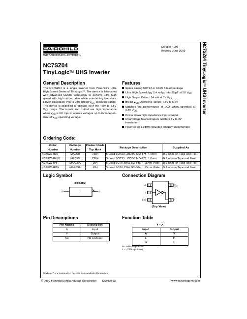
®TinyLogic UHS Two-Input AND GateFeaturesUltra-High Speed: t PD 2.7ns (Typical) into 50pF at 5V V CCHigh Output Drive: ±24mA at 3V V CCBroad V CC Operating Range: 1.65V to 5.5VMatches Performance of LCX Operated at 3.3V V CC Power Down High Impedance Inputs/OutputsOver-Voltage Tolerance inputs facilitate 5V to 3V TranslationProprietary Noise/EMI Reduction CircuitryUltra-Small MicroPak™ PackagesSpace-Saving SOT23 and SC70 Packages DescriptionThe NC7SZ08 is a single two-input AND gate from Fairchild’s Ultra-High Speed (UHS) series of TinyLogic®. The device is fabricated with advanced CMOS technology to achieve ultra-high speed with high output drive while maintaining low static power dissipation over a broad V CC operating range. The devise is specified to operate over the 1.65V to 5.5V V CC operating range. The inputs and output are high impedance when V CC is 0V. Inputs tolerate voltages up to 6V, independent of V CC operating voltage.Ordering InformationPart Number Top Mark Eco Status Package Packing MethodNC7SZ08M5X 7Z08 RoHS 5-Lead SOT23, JEDEC MO-178 1.6mm 3000 Units on Tape & ReelNC7SZ08P5X Z08 RoHS 5-Lead SC70, EIAJ SC-88a, 1.25mm Wide 3000 Units on Tape & ReelNC7SZ08L6X GG RoHS 6-Lead MicroPak™, 1.00mm Wide 5000 Units on Tape & ReelNC7SZ08FHX GG Green 6-Lead,MicroPak2, 1x1mm Body, .35mm Pitch 5000 Units on Tape & ReelFor Fairchild’s definition of Eco Status, please visit: /company/green/rohs_green.html.NC7SZ08 — TinyLogic ® UHS Two-Input AND GateFigure 1. Logic SymbolPin ConfigurationsFigure 2. SC70 and SOT23 (Top View)Figure 3. MicroPak (Top Through View)Pin DefinitionsPin # SC70 / SOT23Pin # MicroPakNameDescription1 1 A Input2 2 B Input3 3 GND Ground4 4 Y Output56 V CC Supply Voltage5 NC No ConnectFunction TableY=ABInputs OutputNC7SZ08 — TinyLogic ® UHS Two-Input AND GateSymbol Parameter Min. Max. UnitV CC Supply Voltage -0.5 6.0 V V IN DC Input Voltage -0.5 6.0 V V OUT DC Output Voltage -0.56.0 V V IN < -0.5V -50 I IK DC Input Diode Current V IN > 6.0V +20 mAV OUT < -0.5V-50I OK DC Output Diode Current V OUT > 6V, V CC =GND+20 mAI OUT DC Output Current±50 mA I CC or I GND DC V CC or Ground Current±50 mA T STG Storage Temperature Range -65 +150 °C T J Junction Temperature Under Bias+150 °C T LJunction Lead Temperature (Soldering, 10 Seconds)+260°CSOT-23 200SC70-5 150MicroPak-6 130 P DPower Dissipation at +85°CMicroPak2-6 120mWHuman Body Model, JESD22-A114 4000 ESD Charged Device Model, JESD22-C1012000VRecommended Operating ConditionsThe Recommended Operating Conditions table defines the conditions for actual device operation. Recommendedoperating conditions are specified to ensure optimal performance to the datasheet specifications. Fairchild does not recommend exceeding them or designing to Absolute Maximum Ratings.Symbol ParameterConditions Min. Max. UnitSupply Voltage Operating 1.65 5.50 V CCSupply Voltage Data Retention1.50 5.50 V V IN Input Voltage 0 5.5VV OUT Output Voltage0 V CC V T A Operating Temperature-40 +85 °C V CC at 1.8V, 2.5V ± 0.2V 0 20® UHS Two-Input AND Gate1.65 1.55 1.65 1.55 1.80 1.70 1.80 1.702.30 2.20 2.30 2.203.00 2.90 3.00 2.904.50V IN =V IH , I OH =-100µA 4.40 4.504.401.65 I OH =-4mA 1.29 1.52 1.292.30 I OH =-8mA 1.90 2.15 1.903.00 I OH =-16mA 2.50 2.80 2.40 3.00 I OH =-24mA 2.40 2.68 2.30VV OHHIGH LevelOutput Voltage4.50 I OH =-32mA 3.90 4.20 3.801.65 0.00 0.10 0.10 1.80 0.00 0.10 0.102.30 0.00 0.10 0.103.00 0.00 0.10 0.104.50V IN =V IL , I OL =100µA 0.00 0.10 0.10 1.65 I OL =4mA 0.80 0.24 0.24 2.30 I OL =8mA 0.10 0.30 0.30 3.00 I OL =16mA 0.15 0.40 0.40 3.00 I OL =24mA 0.22 0.55 0.55 VV OLLOW LevelOutput Voltage4.50 I OL =32mA0.22 0.55 0.55 I IN Input LeakageCurrent0 to 5.5V IN =5.5V, GND±1±10µAI OFF Power OffLeakage Current0 V IN or V OUT =5.5V 1 10 µAI CCQuiescent SupplyCurrent1.65 to 5.50 V IN =5.5V, GND220µA® UHS Two-Input AND Gate5.00 ± 0.500.5 2.2 4.1 0.5 4.4 3.30 ± 0.30 1.53.3 5.2 1.5 5.55.00 ± 0.50 C L =50pF,R L =500Ω0.8 2.7 4.5 0.84.8C IN Input Capacitance 0.00 4 pF 3.30 20 C PDPower DissipationCapacitance (2)5.0025pF Figure 6Note:2. C PD is defined as the value of the internal equivalent capacitance which is derived from dynamic operatingcurrent consumption (I CCD ) at no output lading and operating at 50% duty cycle. C PD is related to I CCD dynamic operating current by the expression: I CCD =(C PD )(V CC )(f IN )+(I CC static).Notes:3. C L includes load and stray capacitance.4. Input PRR=1.0MHz; t W 500ns.Figure 4. AC Test CircuitFigure 5. AC Waveforms=1.8ns; PRR=10MHz; Duty Cycle=50%.Test Circuit® UHS Two-Input AND Gate132LAND PATTERN RECOMMENDATIONC 0.10C0.20C A B0.60 REF0.550.35SEATING PLANE0.25GAGE PLANE8°0°NOTES: UNLESS OTHEWISE SPECIFIEDA) THIS PACKAGE CONFORMS TO JEDEC MO-178, ISSUE B, VARIATION AA,B) ALL DIMENSIONS ARE IN MILLIMETERS. 1.45 MAX1.300.900.150.051.900.950.500.301.502.600.701.00SEE DETAIL A0.220.08C) MA05Brev5TOP VIEW (0.30)Figure 7. 5-Lead SOT23, JEDEC MO-178 1.6mmPackage drawings are provided as a service to customers considering Fairchild components. Drawings may change in any manner without notice. Please note the revision and/or date on the drawing and contact a Fairchild Semiconductor representative to verify or obtain the most recent revision. Package specifications do not expand the terms of Fairchild’s worldwide terms and conditions, specifically the warranty therein, which covers Fairchild products.Always visit Fairchild Semiconductor’s online packaging area for the most recent package drawings: /packaging/.Tape and Reel Specifications®UHS Two-Input AND GateFigure 8. 5-Lead, SC70, EIAJ SC-88a, 1.25mm WidePackage drawings are provided as a service to customers considering Fairchild components. Drawings may change in any mannerwithout notice. Please note the revision and/or date on the drawing and contact a Fairchild Semiconductor representative to verifyor obtain the most recent revision. Package specifications do not expand the terms of Fairchild’s worldwide terms and conditions, specificallythe warranty therein, which covers Fairchild products.Always visit Fairchild Semiconductor’s online packaging area for the most recent package drawings:/packaging/.Tape and Reel Specifications® UHS Two-Input AND Gate2. DIMENSIONS ARE IN MILLIMETERS1. CONFORMS TO JEDEC STANDARD M0-252 VARIATION UAAD MAC06AREVCNotes:3. DRAWING CONFORMS TO ASME Y14.5M-1994TOP VIEWRECOMMENED LAND PATTERNBOTTOM VIEWA0.55MAX0.05C(0.75)(0.52)(0.30)6X 1X6X PIN 1DETAIL A0.075 X 45CHAMFER0.250.150.350.250.400.300.5(0.05) 1.0DETAIL APIN 1 TERMINAL0.400.300.450.350.100.000.10C B A 0.05CC0.05C0.050.005X 5X 6X(0.13)4X6XFigure 9. 6-Lead, MicroPak™, 1.0mm WidePackage drawings are provided as a service to customers considering Fairchild components. Drawings may change in any manner without notice. Please note the revision and/or date on the drawing and contact a Fairchild Semiconductor representative to verify or obtain the most recent revision. Package specifications do not expand the terms of Fairchild’s worldwide terms and conditions, specifically the warranty therein, which covers Fairchild products.Always visit Fairchild Semiconductor’s online packaging area for the most recent package drawings: /packaging/.®UHS Two-Input AND Gate DETAIL A5XFigure 10. 6-Lead, MicroPak2, 1x1mm Body, .35mm PitchPackage drawings are provided as a service to customers considering Fairchild components. Drawings may change in any mannerwithout notice. Please note the revision and/or date on the drawing and contact a Fairchild Semiconductor representative to verifyor obtain the most recent revision. Package specifications do not expand the terms of Fairchild’s worldwide terms and conditions, specificallythe warranty therein, which covers Fairchild products.Always visit Fairchild Semiconductor’s online packaging area for the most recent package drawings:/packaging/.NC7SZ08 — TinyLogic ® UHS Two-Input AND Gate。


西门子选型手册Happy First, written on the morning of August 16, 2022西门子选型手册16ES7212-1AB23-0XB0CPU8I/6O晶体管输出26ES7212-1BB23-0XB0CPU 8I/6O 继电器输出36ES7 212-1AB23-0XB8CPU8I/6O晶体管输出 CN46ES7 212-1BB23-0XB8CPU 8I/6O 继电器输出 CN56ES7 214-1AD23-0XB0CPU14I/10O晶体管输出66ES7 214-1AD23-0XB8CPU14I/10O晶体管输出 CN76ES7 214-1BD23-0XB0CPU14I/10O继电器输出86ES7 214-1BD23-0XB8CPU14I/10O继电器输出 CN96ES7 214-2AD23-0XB0CPU224XP14DI/10DO;2AI;1AO 晶体管输出106ES7 214-2BD23-0XB0CPU224XP 14DI/10DO;2AI;1AO继电器输出116ES7 214-2AD23-0XB8CPU224XP 14DI/10DO;2AI;1AO晶体管输出126ES7 214-2BD23-0XB8CPU224XP 14DI/10DO;2AI;1AO继电器输出136ES7 216-2AD23-0XB0CPU 24I/16O 晶体管输出146ES7 216-2BD23-0XB0CPU24I/16O继电器输出156ES7 216-2AD23-0XB8CPU 24I/16O 晶体管输出 CN166ES7 216-2BD23-0XB8CPU24I/16O继电器输出 CN176ES7 221-1BF22-0XA08点24VDC输入186ES7 221-1BF22-0XA88点24VDC输入 CN196ES7 221-1BH22-0XA016点24VDC输入206ES7 221-1BH22-0XA816点24VDC输入 CN216ES7 222-1HF22-0XA08点继电器输出226ES7 222-1HF22-0XA88点继电器输出 CN236ES7 222-1BF22-0XA08点24VDC输出246ES7 222-1BF22-0XA88点24VDC输出 CN256ES7 223-1PH22-0XA08入8出模块继电器输出266ES7 223-1PH22-0XA88入8出模块继电器输出 CN 276ES7 223-1PL22-0XA016入16出模块继电器输出286ES7 223-1PL22-0XA816入16出模块继电器输出 CN 296ES7 223-1HF22-0XA04入4出模块继电器输出306ES7 223-1HF22-0XA84入4出模块继电器输出 CN 316ES7 223-1BF22-0XA04入4出24VDC326ES7 223-1BF22-0XA84入4出24VDC CN336ES7 223-1BH22-0XA08入8出24VDC346ES7 223-1BH22-0XA88入8出24VDC CN356ES7 223-1BL22-0XA016入16出24VDC366ES7 223-1BL22-0XA816入16出24VDC CN376ES7 231-0HC22-0XA04入模拟量模块386ES7 231-0HC22-0XA84入模拟量模块 CN396ES7 235-0KD22-0XA04入1出模拟量模块406ES7 235-0KD22-0XA84入1出模拟量模块 CN416ES7 232-0HB22-0XA02出模拟量模块426ES7 232-0HB22-0XA82出模拟量模块 CN436ES7 277-0AA22-0XA0PROFIBUS-DP模块446ES7 272-0AA30-0YA0TD 200显示设定单元456ES7 901-3CB30-0XA0计算机编程电缆及软件466ES7 291-8GF23-0XA0EEPROM 64K476ES7 291-8BA20-0XA0电池486ES7 290-6AA20-0XA0 扩展转接电缆 0.8米496ES7 231-7PD22-0XA04路热电耦模块506ES7 231-7PD22-0XA84路热电耦模块 CN516ES7 231-7PB22-0XA02路热电阻模块526ES7 231-7PB22-0XA82路热电阻模块 CN536GK7243-1EX00-0XE0以太网通讯卡西门子可编程SIEMENS S7-300系列序号型号描述16ES7 312-1AE13-0AB0CPU312;16KRAM; MAX 256DI/O;64AI/O;MMC26ES7 312-5BE03-0AB0CPU312C;32KRAM; 本机10I/6O;256DI/O;64AI/O;40PIN36ES7 313-5BF03-0AB0CPU313C;64KRAM;MAX 1016DI/O;253AI/O;2个40PIN<; /P> 46ES7 313-6CF03-0AB0CPU313C-2DP;64KRAM;MAX 8192DI/O;512AI/O;40PIN56ES7 314-1AG13-0AB0CPU314;48KRAM;MAX1024DI/O;256AI/O;MMC66ES7 314-6BG03-0AB0CPU314; 96KRAM;MAX1024DI/O;256AI/O;MMC96ES7 314-6CG03-0AB06ES7 315-2AG10-0AB06ES7 307-1BA00-0AA0CPU314C-2DP;96KRAM;MAX8192DI/O;512AI/O;2个40PIN CPU315-2DP;128KRAM;MAX16384DI/O;1024AI/O;MMCS7-300电源DC24V;2A106ES7 307-1EA00-0AA0S7-300电源DC24V;5A116ES7 307-1KA01-0AA0S7-300电源DC24V;10A126ES7 321-1BL00-0AA0数字输入模块32点入;DC24V136ES7 321-1BH02-0AA0数字输入模块16点入;DC24V146ES7 321-1FF01-0AA08点120V/230VAC 输入156ES7 322-1BL00-0AA0数字输出模块32点出;DC24V;0.5A166ES7 322-1HF01-0AA0数字输出模块8点继电器出;AC220V;2A176ES7 322-1BH01-0AA0数字输出模块16点出;DC24V;0.5A186ES7 322-1HH01-0AA0数字输出模块16点继电器输出2A196ES7 322-1FH00-0AA0数字输出模块16点输出0.5A206ES7 323-1BH01-0AA0数字输入/输出模块;8入/8出;DC24V;0.5A 216ES7 323-1BL00-0AA0数字输入/输出模块;16入/16出;DC24V;0.5A 226ES7 331-7KF02-0AB0模拟量输入模板;8通道;0~10V;4~20MA236ES7 331-7KB02-0AB0模拟量输入模板;2通道246ES7 332-5HD01-0AB0模拟量输出模板;4通道;0~10V;4~20mA256ES7 332-5HB01-0AB0模拟量输出模板;2通道266ES7 340-1AH02-0AE0点对点通讯模板;CP340-1A;带RS232C口276ES7 340-1AH01-7BA0CP340软件手册286ES7 340-1CH02-0AE0点对点通讯模板;CP340-1C;带RS485口296ES7 350-1AH03-0AE0单通道计数模块FM350-1306ES7 350-1AH00-7BG0FM350-1组态软件手册316ES7 350-2AH00-0AE08通道计数模块FM350-2376ES7953-8LF20-0AA06ES7953-8LG11-0AA06ES7953-8LJ20-0AA06ES7953-8LL20-0AA06ES7953-8LM20-0AA06ES7 971-1AA00-0AA0MMC 64KMMC 128KMMC 512KMMC 2MMMC 4M后备电池;3.4V;1AhCPU313;314用386ES7 392-1AJ00-0AA0前连接器;20针396ES7 392-1AM00-0AA0前连接器;40针406ES7 390-1AE80-0AA0导轨;480mm416ES7 390-1AF30-0AA0导轨;530mm426ES7 390-1AJ30-0AA0导轨;830mm436ES7 360-3AA01-0AA0中央模板接口模板446ES7 361-3CA01-0AA0扩展模板接口模板456ES7 365-0BA01-0AA0接口模板一对;带1M电缆466ES7 368-3BB01-0AA0接口模板连接电缆;1M 476ES7 368-3BC51-0AA0接口模板连接电缆;2.5M 486ES7 972-0CB20-0XA0PC MPI电缆496ES7 972-0BA41-0XA0L2网接口不带编程口506ES7 972-0BB41-0XA0L2网接口带编程口516ES7 972-0AA01-0XA0RC485 L2/MPI中继器526GK1 561-1AA01CP5611 PCI通讯卡536GK1 561-3AA01CP5613 PCI通讯卡546GK7 342-5DA02-0XE0CP342-5通讯模块556AV6642-0DA01-1AX0OP177B 5.7寸用户内存2048K 分辨率320×240 256 566AV6642-0DC01-1AX0OP177B 5.7寸用户内存2048K 分辨率320×240 蓝色576AV6 642-0AA01-0AX0TP177A 触摸屏 5.7寸分辨率320×240 蓝色替代TP170A586AV6 642-0BA01-1AX0TP177B 触摸屏 256色替代TP170B596AV6 641-0DD01-1AX0MP277 替代TP270-10 10.4寸用户内存6M 分辨率640×480 按键606ES7 354-1AH01-0AE0FM354 伺服电机定位模块616ES7 355-0VH10-0AE0带4个模拟输出的四通道闭环控制模块 FM355C626ES7 355-1VH10-0AE0用于4个步进或脉冲控制器的闭环控制模块FM355S西门子可编程SIEMENS S7-400系列序号型号描述16ES7400-1TA01-0AA0底板26ES7400-1JA01-0AA0底板36ES7412-2XJ05-0AA0CPU41246ES7414-2XK05-0AB0CPU41456ES7407-0KA01-0AA010A电源66ES7952-1KK00-0AA01M存储器76ES7952-1KL00-0AA02M存储器86ES7971-0BA00后备电池96ES7421-1BL01-0AA032点数字输入;24VDC 106ES7421-7BH01-0AB016点数字输出;24VDC 116ES7422-1BL00-0AA032点数字输出;24VDC 126ES7422-1BH11-0AA016点数字输出;24VDC 136ES7422-1HH00-0AA016点继电器输出146ES7431-7QH00-0AB016点模拟量输入156ES7431-1KF00-0AB08点模拟量输入166ES7431-7KF00-0AB08点模拟量输入176ES7431-7KF10-0AB08点模拟量输出186ES7432-1HF00-0AB08点模拟量输出196ES7460-0AA01-0AB0扩展模块206ES7461-0AA01-0AA0扩展模块216ES7461-0AA00-7AA0终端电阻226ES7468-1BB50-0AA0扩展电缆236ES7492-1AL00-0AA0接线端子。

© 2004 Fairchild Semiconductor Corporation DS012135January 1996Revised August 2004NC7S14 TinyLogic HS Inverter with Schmitt Trigger InputNC7S14TinyLogic HS Inverter with Schmitt Trigger InputGeneral DescriptionThe NC7S14 is a single high performance CMOS Inverter with Schmitt Trigger input. The circuit design provides hys-teresis between the positive-going and negative going input thresholds thereby improving noise margins.Advanced Silicon Gate CMOS fabrication assures high speed and low power circuit operation over a broad V CC range. ESD protection diodes inherently guard both input and output with respect to the V CC and GND rails.Featuress Space saving SOT23 or SC70 5-lead package s Ultra small MicroPak leadless package s Schmitt input hysteresis: > 1V typ s High speed: t PD 4.5 ns typ s Low quiescent power: I CC < 1 µAs Balanced output drive: 2 mA I OL , −2 mA I OH s Broad V CC operating range: 2V – 6V s Balanced propagation delays s Specified for 3V operationOrdering Code:Logic SymbolIEEE/IECPin DescriptionsFunction TableY = AH = HIGH Logic Level L = LOW Logic LevelConnection DiagramsPin Assignments for SC70 and SOT23(Top View)Pad Assignments for MicroPak(Top Thru View)TinyLogic is a registered trademark of Fairchild Semiconductor Corporation.MicroPak is a trademark of Fairchild Semiconductor Corporation.Order Package Package Package DescriptionSupplied AsNumber Number Top Mark NC7S14M5X MA05B 7S145-Lead SOT23, JEDEC MO-178, 1.6mm 3k Units on Tape and Reel NC7S14P5X MAA05A S145-Lead SC70, EIAJ SC-88a, 1.25mm Wide 3k Units on Tape and Reel NC7S14L6XMAC06AUU6-Lead MicroPak, 1.0mm Wide5k Units on Tape and ReelPin NamesDescriptionA Input Y Output NCNo ConnectInput Output A Y L H HL 2N C 7S 14Absolute Maximum Ratings (Note 1)Recommended Operating Conditions (Note 2)Note 1: Absolute maximum ratings are those values beyond which damageto the device may occur. The databook specifications should be met, with-out exception, to ensure that the system design is reliable over its power supply, temperature, and output/input loading variables. Fairchild does not recommend operation of circuits outside the databook specifications.Note 2: Unused inputs must be held HIGH or LOW. They may not float.DC Electrical CharacteristicsSupply Voltage (V CC )−0.5V to +7.0VDC Input Diode Current (I IK ) @V IN ≤ −0.5V −20 mA @V IN ≥ V CC +0.5V +20 mADC Input Voltage (V IN )−0.5V to V CC +0.5VDC Output Diode Current (I OK )@V OUT < −0.5V −20 mA @V OUT > V CC +0.5V +20 mADC Output Voltage (V OUT )−0.5V to V CC +0.5VDC Output Source or Sink Current (I OUT )±12.5 mA DC V CC or Ground Current per Output Pin (I CC or I GND )±25 mAStorage Temperature (T STG )−65°C to +150°CJunction Temperature (T J )150°CLead Temperature (T L )(Soldering,10 seconds)260°CPower Dissipation (P D ) @ +85°C SOT23-5200 mW SC70-5150 mW Supply Voltage (V CC ) 2.0V to 6.0VInput Voltage (V IN )0V to V CCOutput Voltage (V OUT )0V to V CCOperating Temperature (T A )−40°C to +85°CThermal Resistance (θJA )SOT23-5300°C/W SC70-5425°C/W Symbol ParameterV CC T A = +25°CT A = −40°C to +85°C UnitsConditions(V)Min Typ Max Min Max V PPositive Threshold Voltage2.0 1.0 1.29 1.5 1.0 1.6V3.0 1.5 1.90 2.2 1.5 2.24.5 2.3 2.73 3.15 2.3 3.156.03.0 3.564.2 3.0 4.2V NNegative Threshold Voltage2.00.30.700.90.30.9V3.00.6 1.05 1.350.6 1.354.5 1.13 1.66 2.0 1.13 2.06.01.52.24 2.6 1.5 2.6V HHysteresis Voltage2.00.30.59 1.00.3 1.0V3.00.40.85 1.30.4 1.34.50.6 1.08 1.40.6 1.46.00.8 1.31 1.70.8 1.7V OHHIGH Level Output Voltage2.0 1.90 2.0 1.90V3.0 2.90 3.0 2.90I OH = −20 µA4.5 4.40 4.5 4.40V IN = V IL6.0 5.90 6.0 5.90VV IN = V IL3.0 2.68 2.87 2.63I OH = −1.3 mA4.5 4.18 4.37 4.13I OH = −2 mA 6.05.685.86 5.63I OH = −2.6 mAV OLLOW Level Output Voltage2.00.00.100.10V3.00.00.100.10I OH = 20 µA4.50.00.100.10V IN = V IH6.00.00.100.10VV IN = V IH3.00.10.260.33I OL = 1.3 mA4.50.10.260.33I OL = 2 mA 6.00.10.260.33I OL = 2.6 mANC7S14DC Electrical Characteristics (Continued)AC Electrical CharacteristicsNote 3: C PD is defined as the value of the internal equivalent capacitance which is derived from dynamic operating current consumption (I CCD ) at no output loading and operating at 50% duty cycle. (See Figure 2.) C PD is related to I CCD dynamic operating current by the expression: I CCD = (C PD ) (V CC ) (f IN ) + (I CC static).AC Loading and WaveformsC L includes load and stray capacitance Input PRR = 1.0 MHz, t w = 500 nsFIGURE 1. AC Test CircuitInput = AC Waveforms;PRR = variable; Duty Cycle = 50%FIGURE 2. I CCD Test CircuitFIGURE 3. AC WaveformsSymbol ParameterV CC T A = +25°CT A = −40°C to +85°C Units Conditions (V)MinTypMax MinMax I IN Input Leakage Current 6.0±0.1±1.0µA V IN = V CC , GND I CCQuiescent Supply Current6.01.010.0µAV IN = V CC , GNDSymbol ParameterV CC T A = +25°CT A = −40°C to +85°C Units Conditions Figure (V)MinTyp Max MinMaxNumbert PLH Propagation Delay5.0 4.521nsC L = 15 pF Figures 1, 3t PHL2.020100125nsC L = 50 pF3.01227354.58.520256.07.51721t TLH Output Transition Time5.038nsC L = 15 pF Figures 1, 3t THL2.025125145nsC L = 50 pF3.01635454.51125306.092124C IN Input CapacitanceOpen 21010pF C PDPower Dissipation Capacitance5.07pF(Note 3)Figure 2 4N C 7S 14Tape and Reel SpecificationTAPE FORMAT for SC70 and SOT23TAPE DIMENSIONS inches (millimeters)Package TapeNumber Cavity Cover Tape Designator Section Cavities Status Status Leader (Start End)125 (typ)Empty Sealed M5X, P5XCarrier 3000Filled Sealed Trailer (Hub End)75 (typ)EmptySealedPackage Tape Size DIM A DIM B DIM F DIM K o DIM P1DIM W SC70-58 mm 0.0930.0960.138 ±0.0040.053 ±0.0040.1570.315 ±0.004(2.35)(2.45)(3.5 ±0.10)(1.35 ±0.10)(4)(8 ±0.1)SOT23-58 mm0.1300.1300.138 ±0.0020.055 ±0.0040.1570.315 ±0.012(3.3)(3.3)(3.5 ±0.05)(1.4 ±0.11)(4)(8 ±0.3)NC7S14Tape and Reel Specification(Continued)TAPE FORMAT for MircoPakREEL DIMENSIONS inches (millimeters)PackageTape Number Cavity Cover Tape DesignatorSection Cavities Status Status Leader (Start End)125 (typ)Empty Sealed L6XCarrier 5000Filled Sealed Trailer (Hub End)75 (typ)EmptySealedTape Size A B C D N W1W2W38 mm7.00.0590.5120.795 2.1650.331 +0.059/−0.0000.567W1 +0.078/−0.039(177.8)(1.50)(13.00)(20.20)(55.00)(8.40 +1.50/−0.00)(14.40)(W1 +2.00/−1.00) 6N C 7S 14Physical Dimensionsinches (millimeters) unless otherwise noted5-Lead SOT23, JEDEC MO-178, 1.6mmPackage Number MA05B NC7S14Physical Dimensions inches (millimeters) unless otherwise noted (Continued)5-Lead SC70, EIAJ SC-88a, 1.25mm WidePackage Number MAA05A8N C 7S 14 T i n y L o g i c H S I n v e r t e r w i t h S c h m i t t T r i g g e r I n p u tPhysical Dimensions inches (millimeters) unless otherwise noted (Continued)6-Lead MicroPak, 1.0mm Wide Package Number MAC06AFairchild does not assume any responsibility for use of any circuitry described, no circuit patent licenses are implied and Fairchild reserves the right at any time without notice to change said circuitry and specifications.LIFE SUPPORT POLICYFAIRCHILD ’S PRODUCTS ARE NOT AUTHORIZED FOR USE AS CRITICAL COMPONENTS IN LIFE SUPPORT DEVICES OR SYSTEMS WITHOUT THE EXPRESS WRITTEN APPROVAL OF THE PRESIDENT OF FAIRCHILD SEMICONDUCTOR CORPORATION. As used herein:1.Life support devices or systems are devices or systems which, (a) are intended for surgical implant into the body, or (b) support or sustain life, and (c) whose failure to perform when properly used in accordance with instructions for use provided in the labeling, can be rea-sonably expected to result in a significant injury to the user. 2. A critical component in any component of a life support device or system whose failure to perform can be rea-sonably expected to cause the failure of the life support device or system, or to affect its safety or effectiveness.。


iPACS-5762A-G母联(分段)保护测控装置技术说明书版本:V1.01江苏金智科技股份有限公司iPACS-5762A-G母联(分段)保护测控装置技术说明书(V1.01)前言非常感谢您选用江苏金智科技股份有限公司(简称金智科技,股票代码002090)生产的iPACS-5762A-G母联(分段)保护测控装置。
本手册是该保护装置说明书,期望它能为您的工作带来帮助。
本说明书仅供设计选型参考,与实际产品可能存在细微差别,因此不建议作为工程设计依据。
建议工程设计时向我公司设计人员索取相关设计图纸。
如需相关产品、服务和支持的更多信息,请访问金智科技网站/。
本公司有权对本说明书的内容进行定期变更,恕不另行通知。
变更内容将会补充到新版本的说明书中。
_____________________________________________________________版权所有,请勿翻印、复印版本:V1.01iPACS-5762A-G母联(分段)保护测控装置技术说明书(V1.01)目录1 概述 (1)1.1 应用范围 (1)1.2 保护配置和功能 (1)1.2.1 保护配置 (1)1.2.2 测控功能 (1)1.2.3 保护信息功能 (1)2 技术参数 (2)2.1 机械及环境参数 (2)2.1.1 工作环境 (2)2.1.2 机械性能 (2)2.2 电气参数 (2)2.2.1 额定数据 (2)2.2.2 功率消耗 (2)2.2.3 过载能力 (2)2.3 主要技术指标 (2)2.3.1 充电过流保护 (2)2.3.2 零序电流保护 (3)2.3.3 遥信开入 (3)2.3.4 遥测量计量等级 (3)2.3.5 电磁兼容 (3)2.3.6 绝缘试验 (3)2.3.7 输出接点容量 (3)3 软件工作原理 (3)3.1 保护程序结构 (3)3.2 装置起动元件 (4)3.2.1 充电过流I段起动 (4)3.2.2 充电过流II段起动 (4)3.2.3充电零序过流起动 (4)3.3 充电保护 (5)3.3.1 充电过流I段保护 (5)3.3.2 充电过流II段保护 (5)3.3.3 充电零序过流保护 (5)3.4 装置自检 (5)3.5 装置运行告警 (5)iPACS-5762A-G母联(分段)保护测控装置技术说明书(V1.01)3.5.1 TWJ异常判别 (5)3.5.2 弹簧未储能 (5)3.5.3 控制回路断线 (5)3.5.4 TV断线 (5)3.5.5 TA断线 (5)3.5.6 频率异常判别 (5)3.6 遥控、遥测、遥信功能 (6)3.7 对时功能 (6)4 定值内容及整定说明 (7)4.1 系统定值 (7)4.2 保护定值 (7)4.3 通讯参数 (7)4.4 辅助参数 (8)4.5 软压板 (9)5装置接线端子与说明 (10)5.1 出口板全配 (10)5.2 出口板简配 (11)5.3 模拟量输入 (11)5.4 背板接线说明 (11)5.5装置结构及安装参考尺寸 (13)iPACS-5762A-G 母联(分段)保护测控装置技术说明书(V1.01)第 1 页 共 15页1 概述1.1 应用范围iPACS-5762充电保护测控装置可35KV 的母联(分段)开关或进线开关的充电保护和测控功能。
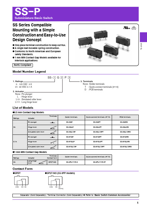
S S -PSS Series Compatible Mounting with a SimpleConstruction and Easy-to-Use Design Concept●One-piece terminal construction to keep out flux. ●A single leaf movable spring construction. ●Conforms to North American and European safety Standards.●1 mm MIN Contact Gap Models available for Interlock applicationsRoHS CompliantModel Number LegendList of Models●0.5 mm Contact Gap Models●1 mm MIN Contact Gap ModelsContact FormSS -@@@1. Ratings3 : 125 VAC 3 A 01 : 30 VDC 0.1 A2. ActuatorNone : Pin plunger L : Hinge leverL13 : Simulated roller lever L111 : Long hinge lever123 3. TerminalsNone : Solder terminalsT : Quick-connect terminals (#110) D : P CB terminalsG P Dummy●SPDT●SPST-NO (SS-3FP models)Separator (Sold Separately), Terminal Connector (Sold Separately)Refer to "Basic Switch Common Accessories "SS-P Subminiature Basic SwitchS S-P Contact Specifications*Please refer to "Using Micro Loads" in "●Precautions" for moreinformation on the minimum applicable load.RatingsNote 1.The above rating values apply under the following test conditions.(1) Ambient temperature: 20±2°C(2) Ambient humidity: 65±5%(3) Operating frequency: 20 operations/minNote 2.Consult your OMRON sales representative for information on modelsfor other loads.Approved Safety StandardsUL (UL1054/CSA C22.2 No.55)VDE (EN61058-1)Testing conditions: 5E4 (50,000 operations) T55 (0 to 55°C) CharacteristicsNote.The data given above are initial values.*1.The values for dielectric strength shown are for models with a Separator (refer to "Micro Switch Common Accessories").*2.The values are at Free Position and Total Travel Position values for pin plunger, and Total Travel Position value for lever.Close or open circuit of the contact is 1 ms max.*3.For testing conditions, consult your OMRON sales representative.Item Model SS-3P models SS-01P models SS-3FP modelsContactSpecification Rivet Crossbar RivetMaterial SilverGoldalloySilverGap(standardvalue)0.5 mm 0.5 mm 1 mm min.InrushcurrentNC9 A max. -9 A max.NOMinimum applicable load(reference value) *5 VDC 160 mA 5 VDC 1 mA 5 VDC 160 mAModelSS-3P /SS-3FP modelsSS-01P modelsRated voltage Item Resistive load125 VAC 3 A 0.1 A30 VDC 3 A 0.1 AModel SS-3P / SS-3FP SS-01PRated voltage Item Resistive load125 VAC 3 A 0.1 A30 VDC 3 A 0.1 ARated voltage Model SS-3P / SS-3FP SS-01P125 VAC 3 A 0.1 A30 VDC 3 A 0.1 AItem Model SS-3P models SS-01P models SS-3FP modelsPermissible operating speed 0.1 mm to 1 m/s (for pin plunger models)PermissibleoperatingfrequencyMechanical 300operations/min Electrical 30operations/min Insulation resistance 100 MΩ min. (at 500 VDC with insulation tester)Contact resistance (initial value) 50 mΩ max. 100 mΩ max. 50 mΩ max.Dielectricstrength *1Between terminals of thesame polarity1,000 VAC 50/60 Hz for 1 minBetween current-carryingmetal parts and ground1,500 VAC 50/60 Hz for 1 minBetween each terminalsand non-current-carryingmetal parts1,500 VAC 50/60 Hz for 1 minVibrationresistance *2Malfunction 10 to 55 Hz, 1.5 mm double amplitudeShockresistanceDurability 1,000m/s2 {approx. 100G} max.Malfunction *2300 m/s2 {approx. 30G} max.Durability *3Mechanical 1,000,000 operations min. (60 operations/min)100,000 operations min.(60 operations/min)Electrical70,000 operations min.(20 operations/min, 125 VAC) 200,000 operations min.(20 operations/min)100,000 operations min.(20 operations/min, 30 VDC)100,000 operations min.(20 operations/min, 30 VDC)Degree of protection IEC IP40Degree of protection against electricshockClass IProof tracking index (PTI) 250Ambient operating temperature -25°C to +85°C (at ambient humidity of 60% max.) (with no icing or condensation)Ambient operating humidity 85% max. (for +5 to +35°C)Weight Approx. 1.6 g (pin plunger models)SS-PSubminiature Basic SwitchS S -PTerminals/Appearances (Unit: mm)Mounting Holes (Unit: mm)Dimensions (Unit: mm) and Operating CharacteristicsThe illustrations and dimensions are for models with solder terminals. Refer to "Terminals/Appearances" for details on models with quick connect terminals (#110) or PCB terminals.Note 1.Unless otherwise specified, a tolerance of ±0.4 mm applies to all dimensions. Note 2.The operating characteristics are for operation in the A direction ().●Solder terminals●Quick Connect Terminals (#110)●PCB terminals<PCB Mounting Dimensions (Reference)>2-2.4 dia. mounting holes ●Pin plunger SS-3GP SS-01GPOperating characteristics Model SS-3GP SS-01GPOperating ForceOF Max. Releasing ForceRFMin.1.50 N {153 gf}0.2 N {20 gf}Pretravel PT Max. Overtravel OT Min. Movement Differential MD Max. 0.6 mm 0.4 mm 0.15 mm Operating PositionOP8.4±0.3 mm●Hinge leverSS-3GLP SS-01GLPOperating characteristics Model SS-3GLP SS-01GLPOperating ForceOF Max.Releasing ForceRFMin.0.5 N {51 gf}0.05 N {5 gf}Overtravel OT Min. Movement Differential MD Max. 1.0 mm 0.8 mmFree PositionFP Max.Operating Position OP13.6 mm 8.8±0.8 mm●Long hinge lever SS-3FL111P-3Operating characteristicsModel SS-3FL111P-3Operating Force OF Max.Releasing Force RFMin.0.55 N {56 gf}0.01 N {1 gf}Overtravel OT Min. Movement Differential MD Max. 1.0 mm 3.0 mm Free PositionFPMax.Operating PositionOP16.8 mm 8.8±1.5 mmSS-PSubminiature Basic SwitchS S -PNote 1.Unless otherwise specified, a tolerance of ±0.4 mm applies to all dimensions. Note 2.The operating characteristics are for operation in the A direction ().Precautions★Please refer to "Common Precautions" for correct use.●Soldering•Connecting to Solder TerminalsComplete the soldering at the iron tip temperature of 350 to 400°C within 5 seconds, and do not apply any external force for 1 minute after soldering. Soldering at an excessively high temperature or soldering for more than 5 seconds may deteriorate the characteristics of the Switch. •Connecting to PCB terminalsWhen using automatic soldering baths, we recommend soldering at 260±5°C within 5 seconds. Make sure that the liquid surface of the solder does not flow over the edge of the board.When soldering terminals manually, complete the soldering at the iron tip temperature between 350 to 400°C within 3 seconds, and do not apply any external force for 1 minute after soldering. When applying solder, keep the solder away from the case of the Switch and do not allow solder or flux to flow into the case.●MountingUse M2.3 mounting screw with plane washers or spring washers to securely mount the Switch. Tighten the screws to a torque of 0.23 to 0.26 N·m {2.3 to 2.7 kgf·cm}.●Using Micro LoadsUsing a model for ordinary loads to open or close the contact of a micro load circuit may result in faulty contact. Use models that operate in the following range. However, even when using micro load models within the following operating range, if inrush current occurs when the contact is opened or closed, it may increase the contact wear and so decrease durability. Therefore, insert a contact protection circuit where necessary. The N-level reference value applies for the minimum applicable load. This value indicates the malfunction reference level for the reliability level of 60% (λ60).(JIS C5003)The equation, λ60=0.5×10⁻⁶/operation indicates that theestimated malfunction rate is less than operations with a reliability level of 60%.●Simulated roller lever SS-3GL13PSS-01GL13POperating characteristicsModel SS-3GL13P SS-01GL13P Operating Force OF Max.Releasing Force RFMin.0.5 N {51 gf}0.05 N {5 gf}Overtravel OT Min. Movement Differential MD Max. 1.0 mm 0.8 mm Free PositionFPMax.Operating PositionOP15.5 mm 10.7±0.8 mmCautionsCorrect Use12,000,000Current (mA)V o l t a g e (V )SS-PSubminiature Basic SwitchS S -P• Application examples provided in this document are for reference only. In actual applications, confirm equipment functions and safety before using the product.• Consult your OMRON representative before using the product under conditions which are not described in the manual or applying the product to nuclear control systems, railroad systems, aviation systems, vehicles, combustion systems, medical equipment, amusement machines, safety equipment, and other systems or equipment that may have a serious influence on lives and property if used improperly. Make sure that the ratings and performance characteristics of the product provide a margin of safety for the system or equipment, and be sure to provide the system or equipment with double safety mechanisms.Cat. No.B108-E1-050716(0207)(O)Note: Do not use this document to operate the Unit.OMRON CorporationElectronic and Mechanical Components CompanyContact: /ecb。


No.DescriptionQty (1)Heated grip harness 1(2)Installation Instruction URL 1(3)Harness boot1(4)Wire tie A (W x L: 7 x 125 mm)3(5)Wire tie B (W x L: 7 x 95 mm)2(6)Wire tie C (W x L: 7 x 165 mm)2(7)Wire tie D (W x L: 7 x 235 mm)2(8)Wire tie E (W x L: 2.5 x 100* mm)2*: Length includes the wire tie head.TOOLS AND SUPPLIES REQUIREDSide cutters Scissors Ruler MarkerElectrical tapePro Honda Handgrip Cement Grease Thread lockIsopropyl alcohol Shop towel(1)(2)RELAY SET Sold separatelyNo.DescriptionQty (1)Fuse (7.5 A)1(2) Relay1HEATED GRIP Sold separatelyNo.DescriptionQty (1) Right heated grip 1(2)Left heated grip1(3) Controller 1(4) Owner’s Manual 1TORQUE INFORMATIONRefer to the Service Manual for the torque values of the removed parts.• To prevent burns, allow the engine, exhaust system, radiator, etc. to cool before installing the accessory. NOTE:• Disconnect the throttle cables from the right grip as instructed in the motorcycle’s Service Manual.• For secure adhesion of the left heated grip to the handlebar, we urge you to use the recommended adhesive agent (Pro Honda Handgrip Cement) and wait until it cures securely.• Be sure to open and close the throttle to check for smooth operation after installation of the right heated grip.• Take care not to damage the painted surfaces of the motorcycle.• Reinstall the removed parts on the motorcycle and make sure that wires and harnesses are not pinched.• Disconnect the negative (-) cable from the battery before installing this accessory.• The memory of the clock will be erased when you disconnect the battery. Reset the clock after reconnecting the battery.• Trim the excess ends off the wire ties after attaching them to the wire harnesses. Do not allow the cut part of the wire tie to interfere with any harness or brake hose.• After heated grip installation, check the lights (e.g.right / left turn signal lights and brake lights) for proper operation.• When replacing any other accessory that is required to install this accessory, follow these instructions only.• Illustrations show the NC700X type, other types are similar.PREPARING THE RELAY SET1. Refer to the Ser vice Manual to remove themotorcycle parts. Disconnect the negative (-) cable from the battery.2. Remove the fuse box cover as shown.2. Remove the left air duct.Open.3. Remove the clip and open the front part of the leftseat cowl slightly as shown.HEATED GRIP INSTALLATION1. Remove the rider and pillion seats.• Confirm the negative (-) cable is disconnected from the battery.4. Remove the left side cover..5. Remove the left front side cowl and disconnect theconnector.6. Connect the controller as shown.7. Disconnect the fuse as shown.9. Install the fuse in the reverse order of removal.10.11. Route the heated grip harness as shown.8. Install and fit the boot over the controller as shown.13. Remove the handlebar weight from the motorcycleas shown.• Repeat on the left side.14. Loosen the bolts and slide the master cylinder asshown.• Be careful not to scratch the handlebar.15. Remove the right handlebar switch as shown.24. Remove the left grip as shown.25. Using isopropyl alcohol, remove all traces ofadhesive from the left handlebar.ISOPROPYL ALCOHOLISOPROPYL ALCOHOL21. Reposition the master cylinder and tighten the boltsas shown.• Be careful not to scratch the handlebar.22. Reinstall the handlebar weight as shown.• Before applying thread lock, thoroughly cleanthe screw.MATING SURFACETORQUE: 12 N·m(1.2 kgf·m, 9 lbt·ft)THREAD LOCKBe sure to apply to the threads of the screw.(Reuse)23. Open and close the throttle grip as shown.• Check that the throttle opens and automatically closes smoothly.29. Slide the left heated grip onto the left handlebar as Array indicated.• Wipe up excess adhesive at once.<NC700X>• Before applying thread lock, thoroughly clean 31. Secure the heated grip harness as shown.WIRE TIE BHARNESS(Reuse)34. Secure each harness with the wire ties as shown.• Secure while the handlebar is turned right fully. After securing, move the handlebar right and left and check that the harnesses are not pinched by the neighboring components and that they are not pulled taut.Secure the heated grip, left heated grip andmotorcycle’s harnesses to the handlebar.35. Connect each harness as shown.harness at the marked point to the motorcycle’s harness.38. Secure the right heated grip harness as shown.• Open and close the throttle and confirm that there is no tightness of the heated grip harness.DEALER TROUBLESHOOTING• Stop the engine and turn the ignition switch OFF when you check the parts and circuits other than those of the heated grips.39. Check each harness for sufficient play.• Move the handlebar right and left and check that the harnesses are not pinched by the neighboring components and that they are not pulled taut.40. Install the motorcycle’s parts in the reverse order ofremoval.• Confirm that the harness is not caught or too tight.41. Move the handlebar right and left, and check thatthis accessory is not interfere with the motorcycle parts.。
