SMCJ150CA中文资料
- 格式:pdf
- 大小:80.67 KB
- 文档页数:3

POWER: 1500Wa t VOLTAGE RANGE: 6.8 - 440 VAXIAL LEADED TRANSIENT VOLTAGE SUPPRESS DIODE1.5KE6.8A(CA) - 1.5KE440A(CA)6.8V – 440V Standoff VoltageCase: JEDEC DO-201AD Molded Plastic FeaturesGlass Passivated Die Construction Uni- and Bi-Directional Versions Available Excellent Clamping Capability Fast Response TimePlastic Case Material has UL FlammabilityMechanical DataTerminals: Axial Leads, Solderable per MIL-STD-202, Method 208 Polarity: Cathode Band or Cathode Notch Marking:Unidirectional – Device Code and Cathode Band Bidirectional – Device Code OnlyMaximum Ratings and Electrical Characteristics@T A =25°C unless otherwise specifiedCharacteristicSymbol Value Unit Peak Pulse Power Dissipation at T A = 25°C (Note 1, 2, 5) Figure 3P PPM 1500 MinimumW Peak Forward Surge Current (Note 3)I FSM 200A Peak Pulse Current on 10/1000µS Waveform (Note 1) Figure 1I PPM See Table 1A Steady State Power Dissipation (Note 2, 4)P M(AV) 5.0W Operating and Storage Temperature RangeT j , T STG-65 to +175°CNote: 1. Non-repetitive current pulse, per Figure 1 and derated above T A = 25°C per Figure 4.2. Mounted on 40mm 2 copper pad.3. 8.3ms single half sine-wave duty cycle = 4 pulses per minutes maximum.4. Lead temperature at 75°C = T L .5. Peak pulse power waveform is 10/1000µS.!!!!!!!Weight: 1.20 grams (approx.)!森美特94.085.57.0211.4510.513.4 1.5KE440CA1.5KE400CA 1.5KE350A 1.5KE220CA 1.5KE170CA 1.5KE150A 1.5KE82CA (uA)R RMW RMW@V leakage Reverse CurrentPulse Peak (A)Vc(V)(mA)BR MAX CurrentMax.BR MIN @I Min.Volgtage Breakdown (V)(BI)(Uni)Voltage Stand-Off Reverse Maximum Clamping V T PP(V)V @I Volgtage Breakdown Test (V)V T Volgtage @I PP 1.5KE62CA 1.5KE56CA 1.5KE51CA 1.5KE47CA 1.5KE43CA 1.5KE39CA 1.5KE36CA 1.5KE33CA 1.5KE30CA 1.5KE27CA 1.5KE24CA 1.5KE22CA 1.5KE20CA 1.5KE18CA 1.5KE16CA 1.5KE15CA 1.5KE13CA 1.5KE12CA 1.5KE11CA 1.5KE10CA 1.5KE9.1CA 1.5KE8.2CA 1.5KE7.5CA 1.5KE6.8CA 1.5KE6.8A 1.5KE7.5A 1.5KE8.2A 1.5KE9.1A 1.5KE10A 1.5KE11A 1.5KE12A 1.5KE13A 1.5KE15A 1.5KE16A 1.5KE18A 1.5KE20A 1.5KE22A 1.5KE24A 1.5KE27A 1.5KE30A 1.5KE33A1.5KE36A 1.5KE39A 1.5KE43A 1.5KE47A 1.5KE51A 1.5KE56A 1.5KE300CA 1.5KE250CA 1.5KE200CA 1.5KE180CA 1.5KE160CA 1.5KE150CA 1.5KE130CA 1.5KE120CA 1.5KE110CA 1.5KE100CA 1.5KE91CA 1.5KE75CA 1.5KE68CA 1.5KE62A 1.5KE68A 1.5KE75A 1.5KE82A 1.5KE91A 1.5KE100A 1.5KE110A 1.5KE120A 1.5KE130A 1.5KE160A 1.5KE170A 1.5KE180A 1.5KE200A 1.5KE220A 1.5KE250A 1.5KE300A 1.5KE400A 1.5KE440A1.5KE350CA 5.80 6.45 7.14 10 144.8 1000.06.407.13 7.88 10 11.3 134.5 500.0 7.79 8.61 10 12.1 125.6 200.0 7.78 8.65 9.55 1.0 113.4 50.0 8.55 9.50 10.5 1.0 14.5 104.8 10.0 9.40 10.11.6 1.0 15.6 97.4 5.0 10.212.6 1.0 16.7 91.0 5.011.1 12.4 13.7 1.0 18.2 83.5 5.0 12.8 14.3 15.8 1.0 21.2 71.75.013.615.2 16.8 1.0 22.5 67.6 5.0 15.3 17.1 18.9 1.0 25.2 60.3 5.0 17.1 19.0 21.0 1.0 27.7 54.9 5.0 18.820.923.1 1.0 30.6 49.7 5.020.5 22.8 25.2 1.0 33.2 45.8 5.023.1 25.7 28.4 1.0 37.5 40.5 5.0 25.6 28.5 31.5 1.0 41.4 36.7 5.0 28.2 31.4 34.7 1.0 45.7 33.3 5.030.8 34.2 37.8 1.0 49.9 30.5 5.033.3 37.1 41.0 1.0 53.9 28.2 5.0 36.8 40.9 45.2 1.0 59.3 25.6 5.0 40.2 44.7 49.4 1.0 64.8 23.5 5.0 43.648.553.6 1.0 70.1 21.7 5.047.8 53.2 58.8 1.0 77.0 19.7 5.053.0 58.9 65.1 1.0 85.0 17.9 5.058.1 64.6 71.4 1.0 92.0 16.5 5.0 64.1 71.3 78.8 1.0 103 14.8 5.0 70.1 77.9 86.1 1.0 113 13.5 5.0 77.8 86.5 95.5 1.0 125 12.2 5.095.0 105 1.0 137 11.1 5.0105 116 1.0 152 10.0 5.0102 114 126 1.0 165 9.2 5.0 111 124 137 1.0 179 8.5 5.0128 143 158 1.0 207 7.3 5.0136 152 168 1.0 219 6.9 5.0 145 162 179 1.0 234 6.5 5.0 154 171 189 1.0 246 6.2 5.0 171 190 210 1.0 274 5.5 5.0 185 209 231 1.0 328 4.6 5.0 214 237 263 1.0 344 4.4 5.0256 285 315 1.0 414 3.7 5.0300 333 368 1.0 482 3.2 5.0 342 380 420 1.0 548 2.8 5.0 376 418 462 1.0 600 2.5 5.0TYPE森美特255075100125150175200100755025T ,AMBIENT TEMPERATURE (°C)Fig.4Pulse Derating CurveA P K P U L S E D E R A T I N G (%P K P W R O R C U R R E N T )25507510012515017520002.55.0T ,LEAD TEMPERATURE (°C)Fig.5,Steady State Power DeratingLP ,S T E A D Y S T A T E P O W E R D I S S I P A T I O N (W )d 0.11.0T ,PULSE WIDTH (µs)Fig.3Pulse Rating Curvep 0.1101001.010100100010000P ,P E A K P U L S E P O W E R (k W )P0123I ,P E A K P U L S E C U R R E N T (%)P p pt,TIME (ms)Fig.1Pulse Waveform110100100010100100010,000V ,REVERSE STANDOFF VOLTAGE (V)Fig.2Typical Junction CapacitanceRWM C ,C A P A C I T A N C E (p F )j 森美特。

SA5.0(C)A - SA170(C)A1:1Scale 1:1 on letter size paperDimensions shown below are in:inches [millimeters]Part Weight per unit (gram): 0.4TRADEMARKSACEx™CoolFET™CROSSVOLT™E 2CMOS TM FACT™FACT Quiet Series™FAST ®FASTr™GTO™HiSeC™The following are registered and unregistered trademarks Fairchild Semiconductor owns or is authorized to use and is not intended to be an exhaustive list of all such trademarks.LIFE SUPPORT POLICYFAIRCHILD’S PRODUCTS ARE NOT AUTHORIZED FOR USE AS CRITICAL COMPONENTS IN LIFE SUPPORTDEVICES OR SYSTEMS WITHOUT THE EXPRESS WRITTEN APPROV AL OF FAIRCHILD SEMICONDUCTOR CORPORA TION.As used herein:ISOPLANAR™MICROWIRE™POP™PowerTrench™QS™Quiet Series™SuperSOT™-3SuperSOT™-6SuperSOT™-8TinyLogic™1. Life support devices or systems are devices or systems which, (a) are intended for surgical implant intothe body, or (b) support or sustain life, or (c) whosefailure to perform when properly used in accordancewith instructions for use provided in the labeling, can be reasonably expected to result in significant injury to the user.2. A critical component is any component of a lifesupport device or system whose failure to perform can be reasonably expected to cause the failure of the life support device or system, or to affect its safety or effectiveness.PRODUCT STATUS DEFINITIONS Definition of Terms Datasheet Identification Product Status DefinitionAdvance InformationPreliminary No Identification Needed Obsolete This datasheet contains the design specifications for product development. Specifications may change in any manner without notice.This datasheet contains preliminary data, andsupplementary data will be published at a later date.Fairchild Semiconductor reserves the right to make changes at any time without notice in order to improve design.This datasheet contains final specifications. Fairchild Semiconductor reserves the right to make changes at any time without notice in order to improve design.This datasheet contains specifications on a product that has been discontinued by Fairchild semiconductor.The datasheet is printed for reference information only.Formative or In DesignFirst ProductionFull ProductionNot In ProductionDISCLAIMERFAIRCHILD SEMICONDUCTOR RESERVES THE RIGHT TO MAKE CHANGES WITHOUT FURTHER NOTICE TO ANY PRODUCTS HEREIN TO IMPROVE RELIABILITY , FUNCTION OR DESIGN. FAIRCHILD DOES NOT ASSUME ANY LIABILITY ARISING OUT OF THE APPLICATION OR USE OF ANY PRODUCT OR CIRCUIT DESCRIBED HEREIN; NEITHER DOES IT CONVEY ANY LICENSE UNDER ITS PATENT RIGHTS, NOR THE RIGHTS OF OTHERS.UHC™VCX™。
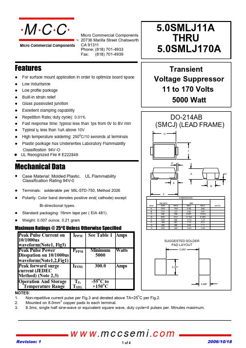
FeaturesMechanical DataTerminals: solderable per MIL-STD-750, Method 2026 Polarity: Color band denotes positive end( cathode) exceptBi-directional types.Standard packaging: 16mm tape per ( EIA 481). Weight: 0.007 ounce, 0.21 gramMaximum Ratings @ 25o C Unless Otherwise SpecifiedPeak Pulse Current on 10/1000uswaveform(Note1, Fig3)I PPM See Table 1Amps Peak Pulse Power Disspation on 10/1000us waveform(Note1,2,Fig1)P PPMMinimum 5000Watts Peak forward surge current (JEDEC Method) (Note 2,3)I FSM)300.0Amps Operation And Storage Temperature Range T J ,T STG -55o C to +150o CNOTES:1.Non-repetitive current pulse per Fig.3 and derated above TA=25oC per Fig.2.2.Mounted on 8.0mm 2copper pads to each terminal.3.8.3ms, single half sine-wave or equivalent square wave, duty cycle=4 pulses per. Minutes maximum.For surface mount application in order to optimize board space Low inductance Low profile package Built-in strain relief Glass passivated junction Excellent clamping capability Repetition Rate( duty cycle): 0.01%Fast response time: typical less than 1ps from 0V to BV min Typical I D less than 1uA above 10VHigh temperature soldering: 250oC/10 seconds at terminals Plastic package has Underwrites Laboratory FlammabilityClassification 94V-Oomp onents 20736 Marilla Street Chatsworth! "# $ % ! "#Revision: 1 2006/10/18 UL Recognized File # E222849TMMicro Commercial ComponentsCase Material: Molded Plastic. UL Flammability Classification Rating 94V-0www.mccsemi .com1 of 4MAXIMUM CLAMPING VOLTAGE REVERSE LEAKAGE @Ipp @V RWM Vc(V)I D (µA)5.0SMLJ 11A 1112.213.51018.22758005PEN 5.0SMLJ 12A 1213.314.71019.92528005PEP 5.0SMLJ 13A 1314.415.91021.52335005PEQ 5.0SMLJ 14A 1415.617.21023.22162005PER 5.0SMLJ 15A 1516.718.5124.42051005PES 5.0SMLJ 16A 1617.819.7126193505PET 5.0SMLJ 17A 1718.920.9127.6181205PEU 5.0SMLJ 18A 182022.1129.2172105PEV 5.0SMLJ 20A 2022.224.5132.415555PEW 5.0SMLJ 22A 2224.426.9135.514155PEX 5.0SMLJ 24A 2426.729.5138.912955PEZ 5.0SMLJ 26A 2628.931.9142.111955PFE 5.0SMLJ 28A 2831.134.4145.411055PFG 5.0SMLJ 30A 3033.336.8148.410355PFK 5.0SMLJ 33A 3336.740.6153.393.955PFM 5.0SMLJ 36A 364044.2158.186.155PFP 5.0SMLJ 40A 4044.449.1164.577.655PFR 5.0SMLJ 43A 4347.852.8169.472.155PFT 5.0SMLJ 45A 455055.3172.768.855PFV 5.0SMLJ 48A 4853.358.9177.464.755PFX 5.0SMLJ 51A 5156.762.7182.460.755PFZ 5.0SMLJ 54A 546066.3187.157.555RGE 5.0SMLJ 58A 5864.471.2193.653.555PGG 5.0SMLJ 60A 6066.773.7196.851.755PGK 5.0SMLJ 64A 6471.178.6110348.655PGM 5.0SMLJ 70A 7077.886111344.355PGP 5.0SMLJ 75A 7583.392.1112141.455PGR 5.0SMLJ 78A 7886.795.8112639.755PGT 5.0SMLJ 85A 8594.4104113736.555PGV 5.0SMLJ 90A 90100111114634.355PGX 5.0SMLJ 100A 100111123116230.955PGZ 5.0SMLJ 110A 110122135117728.355PHE 5.0SMLJ 120A 12013314711932655PHG 5.0SMLJ 130A 13014415912092455PHK 5.0SMLJ 150A 150167185124320.655PHM 5.0SMLJ 160A 160178197125919.355PHP 5.0SMLJ 170A170189209127518.255PHRDEVICE MARKING CODE PART NUMBERPEAK PULSE CURRENT Ipp (A)TEST CURRENT I T (mA)BREAKDOWNVOLTAGE V BR (V)MAX.@ITBREAKDOWN VOLTAGEV BR (V)MIN.@IT REVERSE STAND- OFF VOLTAGE V RWM (V)TMMicro Commercial Components5.0SMLJ11A~5.0SMLJ170Awww.mccsemi .com2 of 4Revision: 1 2006/10/18MAXIMUM CLAMPING VOLTAGE REVERSE LEAKAGE @Ipp @V RWM Vc(V)I D (µA)5.0SMLJ 11CA 1112.213.51018.22758005BEN 5.0SMLJ 12CA 1213.314.71019.92528005BEP 5.0SMLJ 13CA 1314.415.91021.52335005BEQ 5.0SMLJ 14CA 1415.617.21023.22162005BER 5.0SMLJ 15CA 1516.718.5124.42051005BES 5.0SMLJ 16CA 1617.819.7126193505BET 5.0SMLJ 17CA 1718.920.9127.6181205BEU 5.0SMLJ 18CA 182022.1129.2172105BEV 5.0SMLJ 20CA 2022.224.5132.415555BEW 5.0SMLJ 22CA 2224.426.9135.514155BEX 5.0SMLJ 24CA 2426.729.5138.912955BEZ 5.0SMLJ 26CA 2628.931.9142.111955BFE 5.0SMLJ 28CA 2831.134.4145.411055BFG 5.0SMLJ 30CA 3033.336.8148.410355BFK 5.0SMLJ 33CA 3336.740.6153.393.955BFM 5.0SMLJ 36CA 364044.2158.186.155BFP 5.0SMLJ 40CA 4044.449.1164.577.655BFR 5.0SMLJ 43CA 4347.852.8169.472.155BFT 5.0SMLJ 45CA455055.3172.768.855BFVPART NUMBERREVERSE STAND- OFF VOLTAGE V RWM (V)BREAKDOWN VOLTAGEV BR (V)MIN.@IT BREAKDOWNVOLTAGE V BR (V)MAX.@ITTEST CURRENT I T (mA)PEAK PULSE CURRENT Ipp (A)DEVICE MARKING CODE TMMicro Commercial Components5.0SMLJ11C A~5.0SMLJ 45C AFor Bidirectional type having Vrwm of 20 volts and less,the Ir limit is double.www.mccsemi .com3 of 4Revision: 1 2006/10/18Revision: 12006/10/18Micro Commercial Componentswww.mccsemi .com4 of 4products are represented on our website, harmless against all damages.***APPLICATIONS DISCLAIMER******IMPORTANT NOTICE***Aerospace or Military Applications.Products offer by Micro Commercial Components Corp .are not intended for use in Medical,Micro Commercial Components Corp .reserve s the right to make changes without further notice to any product herein to make corrections, modifications , enhancements , improvements , or other changes .Micro Commercial Components Corp .does not assume any liability arising out of the application or use of any product described herein; neither does it convey any license under its patent rights ,nor the rights of others . The user of products in such applications shall assume all risks of such use and will agree to hold Micro Commercial Components Corp .and all the companies whose。


横河CA150中文说明
日本横河(YOKOGAWA)CA150便携式过程校验仪突出特点
多功能、高精度校准仪通常用于校准、测试工业过程装置及各种电气设备。
手持立式校准仪:
立式易持设计使本产品易于直观操作,通过按键能直接进入各自功能。
使用主机套(型号名:93027)时,你可以将CA150挂在身上或者手边的栏杆上。
信号源和测量操作同时进行:
王常规校准应用中,需要多个设备,如标准源、电阻箱和万用表。
现在,只要用一台CA150,既能对热电偶、热电阻和仪表执行常规检查和维护,又能付过程装置,如变送器、温度调节器和信号变换器进行维护和设备诊断。
高精度、多功能的源和测量:
对于源单元和测量单元的直流电压量程具有0.02%高精度。
具有直流电压、直流电流、电阻、热电阻、热电偶(10种)和频率等测量功能。
在DC1V、0V、500欧姆(激励电流1mA)和RTD(激励电流1mA)量程,源响应时间zui小5ms。
环路供电功能:
向环路供电(最大22mADC)时,能够测量来自2线制变送器的电流信号。


S M B J15C A中文资料(总5页) -CAL-FENGHAI.-(YICAI)-Company One1-CAL-本页仅作为文档封面,使用请直接删除SMBJ5.0(C)A - SMBJ440(C)A600W Surface Mount Transient Voltage Suppressor Features600W Peak Pulse Power Dissipation5.0V - 440V Standoff VoltagesGlass Passivated Die ConstructionUni- and Bi-Directional Versions Available Excellent Clamping CapabilityFast Response TimePlastic Material - UL FlammabilityClassification Rating 94V-0Mechanical DataCase: SMB, Transfer Molded EpoxyTerminals: Solderable per MIL-STD-202,Method 208Polarity Indicator: Cathode Band(Note: Bi-directional devices have no polarityindicator.)Marking: Date Code and Marking CodeSee Page 2Weight: 0.1 grams (approx.)MAXIMUM RATINGSRating at Ta = 25 C ambient temperature unless otherwise specified.DO-214AA (SMB)0.083(2.11) 0.155(3.94) 0.075(1.91) 0.130(3.30)0.185(4.70)0.160(4.06)0.012(0.31)0.006(0.15) 0.096(2.44)0.083(2.13)0.050(1.27) 0.008(0.203)0.030(0.76) MAX.0.220(5.59)0.200(5.08)Dimensions in inches and (millimeters)Rating Symbol Value UnitsPeak Pulse Power Dissipation on 10/1000μs (1)waveform (Notes 1, 2, Fig. 3) P PPM Minimum 600 Watts Peak Pulse Current on 10/1000μswaveform (Note 1, Fig. 5) I PPM See Table Amps Peak forward Surge Current8.3 ms single half sine-wave superimposed onrated load ( JEDEC Method )(Notes 2, 3)Maximum Instantaneous Forward Voltage at 50A V FM See Note 3, 4 VoltsOperating Junction and Storage Temperature Range T J, T STG - 65 to + 150 C Note :(1) Non-repetitive Current pulse, per Fig. 5 and derated above Ta = 25 C per Fig. 1(2) Mounted on 5.0mm2 (0.013mm thick) land areas.(3) Measured on 8.3ms. Single half sine-wave or equivalent square wave, duty cycle = 4 pulses per minutes maximum.SMBJ15CATYPE MarkingReverse Breakdown Stand-Off Voltage Voltage Min. @I T BreakdownVoltage TestMax. @ I T CurrentMaximumClampingVoltage@I PPPeak ReversePulse LeakageCurrent @V RMW(Uni) (BI) (Uni) (Bi) V (V) V(V) V(V) I T (mA) V(V) I PP(A) I R(uA) SMBJ5.0 SMBJ5.0C KD AD 5.0 6.40 7.55 10 9.6 62.5 800.0 SMBJ5.0A SMBJ5.0CA KE AE 5.0 6.40 7.25 10 9.2 65.2 800.0 SMBJ6.0 SMBJ6.0C KF AF 6.0 6.67 8.45 10 11.4 52.6 800.0 SMBJ6.0A SMBJ6.0CA KG AG 6.0 6.67 7.67 10 10.3 58.3 800.0 SMBJ6.5 SMBJ6.5C KH AH 6.5 7.22 9.14 10 12.3 48.8 500.0 SMBJ6.5A SMBJ6.5CA KK AK 6.5 7.22 8.30 10 11.2 53.6 500.0 SMBJ7.0 SMBJ7.0C KL AL 7.0 7.78 9.86 10 13.3 45.1 200.0 SMBJ7.0A SMBJ7.0CA KM AM 7.0 7.78 8.95 10 12.0 50.0 200.0 SMBJ7.5 SMBJ7.5C KN AN 7.5 8.33 10.67 1.0 14.3 42.0 100.0 SMBJ7.5A SMBJ7.5CA KP AP 7.5 8.33 9.58 1.0 12.9 46.5 100.0 SMBJ8.0 SMBJ8.0C KQ AQ 8.0 8.89 11.3 1.0 15.0 40.0 50.0 SMBJ8.0A SMBJ8.0CA KR AR 8.0 8.89 10.23 1.0 13.6 44.1 50.0 SMBJ8.5 SMBJ8.5C KS AS 8.5 9.44 11.92 1.0 15.9 37.7 20.0 SMBJ8.5A SMBJ8.5CA KT AT 8.5 9.44 10.82 1.0 14.4 41.7 20.0 SMBJ9.0 SMBJ9.0C KU AU 9.0 10.0 12.6 1.0 16.9 35.5 10.0 SMBJ9.0A SMBJ9.0CA KV AV 9.0 10.0 11.5 1.0 15.4 39.0 10.0 SMBJ10 SMBJ10C KW AW 10 11.1 14.1 1.0 18.8 31.9 5.0 SMBJ10A SMBJ10CA KX AX 10 11.1 12.8 1.0 17.0 35.3 5.0 SMBJ11 SMBJ11C KY AY 11 12.2 15.4 1.0 20.1 29.9 5.0 SMBJ11A SMBJ11CA KZ AZ 11 12.2 14.0 1.0 18.2 33.0 5.0 SMBJ12 SMBJ12C LD BD 12 13.3 16.9 1.0 22.0 27.3 5.0 SMBJ12A SMBJ12CA LE BE 12 13.3 15.3 1.0 19.9 30.2 5.0 SMBJ13 SMBJ13C LF BF 13 14.4 18.2 1.0 23.8 25.2 5.0 SMBJ13A SMBJ13CA LG BG 13 14.4 16.5 1.0 21.5 27.9 5.0 SMBJ14 SMBJ14C LH BH 14 15.6 19.8 1.0 25.8 23.3 5.0 SMBJ14A SMBJ14CA LK BK 14 15.6 17.9 1.0 23.2 25.9 5.0 SMBJ15 SMBJ15C LL BL 15 16.7 21.1 1.0 26.9 22.3 5.0 SMBJ15A SMBJ15CA LM BM 15 16.7 19.2 1.0 24.4 24.6 5.0 SMBJ16 SMBJ16C LN BN 16 17.8 22.6 1.0 28.8 20.8 5.0 SMBJ16A SMBJ16CA LP BP 16 17.8 20.5 1.0 26.0 23.1 5.0 SMBJ17 SMBJ17C LQ BQ 17 18.9 23.9 1.0 30.5 19.7 5.0 SMBJ17A SMBJ17CA LR BR 17 18.9 21.7 1.0 27.6 21.7 5.0 SMBJ18 SMBJ18C LS BS 18 20.0 25.3 1.0 32.2 18.6 5.0 SMBJ18A SMBJ18CA LT BT 18 20.0 23.3 1.0 29.2 20.5 5.0 SMBJ20 SMBJ20C LU BU 20 22.2 28.1 1.0 35.8 16.8 5.0 SMBJ20A SMBJ20CA LV BV 20 22.2 25.5 1.0 32.4 18.5 5.0 SMBJ22 SMBJ22C LW BW 22 24.4 30.9 1.0 39.4 15.2 5.0 SMBJ22A SMBJ22CA LX BX 22 24.4 28.0 1.0 35.5 16.9 5.0 SMBJ24 SMBJ24C LY BY 24 26.7 33.8 1.0 43.0 14.0 5.0 SMBJ24A SMBJ24CA LZ BZ 24 26.7 30.7 1.0 38.9 15.4 5.0 SMBJ26 SMBJ26C MD CD 26 28.9 36.6 1.0 46.6 12.9 5.0 SMBJ26A SMBJ26CA ME CE 26 28.9 33.2 1.0 42.1 14.3 5.0 SMBJ28 SMBJ28C MF CF 28 31.1 39.4 1.0 50.0 12.0 5.0 SMBJ28A SMBJ28CA MG CG 28 31.1 35.8 1.0 45.4 13.2 5.0 Note:( 1 ) V measured after I applied for 300 s., I = square wave pulse or equivalent. ( 2 )Surge Current Waveform per Figure 5 and Derate per Figure 1( 3 ) A Transient suppressor is normally selected according to the reverse " Stand-off Voltage " (V) which should beequal to or greater then the D.C. or continuous peak operating voltage level.SMBJ15CAReverse Breakdown Breakdown Maximum Peak Reverse TYPE Marking Stand-Off Voltage Voltage Test Clamping Pulse LeakageVoltage Min. @I T Max. @ I T Current Voltage @I Current @V RMW (Uni) (BI) (Uni) (Bi) V (V) V(V) V(V) I T (mA) V(V) I PP(A) I R(uA) SMBJ30 SMBJ30C MH CH 30 33.3 42.2 1.0 53.5 11.2 5.0 SMBJ30A SMBJ30CA MK CK 30 33.3 38.3 1.0 48.4 12.4 5.0 SMBJ33 SMBJ33C ML CL 33 36.7 46.5 1.0 59.0 10.2 5.0 SMBJ33A SMBJ33CA MM CM 33 36.7 42.2 1.0 53.3 11.3 5.0 SMBJ36 SMBJ36C MN CN 36 40.0 50.7 1.0 64.3 9.3 5.0 SMBJ36A SMBJ36CA MP CP 36 40.0 46.0 1.0 58.1 10.3 5.0 SMBJ40 SMBJ40C MQ CQ 40 44.4 56.3 1.0 71.4 8.4 5.0 SMBJ40A SMBJ40CA MR CR 40 44.4 51.1 1.0 64.5 9.3 5.0 SMBJ43A SMBJ43CA MT CT 43 47.8 54.9 1.0 69.4 8.6 5.0 SMBJ45 SMBJ45C MU CU 45 50.0 63.3 1.0 80.3 7.5 5.0 SMBJ45A SMBJ45CA MV CV 45 50.0 57.5 1.0 72.7 8.3 5.0 SMBJ48 SMBJ48C MW CW 48 53.3 67.5 1.0 85.5 7.0 5.0 SMBJ48A SMBJ48CA MX CX 48 53.3 61.3 1.0 77.4 7.8 5.0 SMBJ51 SMBJ51C MY CY 51 56.7 71.8 1.0 91.1 6.6 5.0 SMBJ51A SMBJ51CA MZ CZ 51 56.7 65.2 1.0 82.4 7.3 5.0 SMBJ54 SMBJ54C ND DD 54 60.0 76.0 1.0 96.3 6.2 5.0 SMBJ54A SMBJ54CA NE DE 54 60.0 69.0 1.0 87.1 6.9 5.0 SMBJ58 SMBJ58C NF DF 58 64.4 81.6 1.0 103 5.8 5.0 SMBJ58A SMBJ58CA NG DG 58 64.4 74.1 1.0 93.6 6.4 5.0 SMBJ60 SMBJ60C NH DH 60 66.7 84.5 1.0 107 5.6 5.0 SMBJ60A SMBJ60CA NK DK 60 66.7 76.7 1.0 96.8 6.2 5.0 SMBJ64 SMBJ64C NL DL 64 71.1 90.1 1.0 114 5.3 5.0 SMBJ64A SMBJ64CA NM DM 64 71.1 81.8 1.0 103 5.8 5.0 SMBJ70 SMBJ70C NN DN 70 77.8 98.6 1.0 125 4.8 5.0 SMBJ70A SMBJ70CA NP DP 70 77.8 89.5 1.0 113 5.3 5.0 SMBJ75 SMBJ75C NQ DQ 75 83.0 105.7 1.0 134 4.5 5.0 SMBJ75A SMBJ75CA NR DR 75 83.0 95.8 1.0 121 5.0 5.0 SMBJ90 SMBJ90C NW DW 90 100 126.5 1.0 160 3.8 5.0 SMBJ90A SMBJ90CA NX DX 90 100 115.5 1.0 146 4.1 5.0 SMBJ100 SMBJ100C NY DY 100 111 141.0 1.0 179 3.4 5.0 SMBJ100A SMBJ100CA NZ DZ 100 111 128.0 1.0 162 3.7 5.0 SMBJ110 SMBJ110C PD ED 110 122 154.5 1.0 196 3.1 5.0 SMBJ110A SMBJ110CA PE EE 100 122 140.5 1.0 177 3.4 5.0 SMBJ120 SMBJ120C PF EF 120 133 169.0 1.0 214 2.8 5.0 SMBJ120A SMBJ120CA PG EG 120 133 153.0 1.0 193 3.1 5.0 SMBJ130 SMBJ130C PH EH 130 144 182.5 1.0 231 2.6 5.0 SMBJ130A SMBJ130CA PK EK 130 144 165.5 1.0 209 2.9 5.0 SMBJ150 SMBJ150C PL EL 150 167 211.5 1.0 268 2.2 5.0 SMBJ150A SMBJ150CA PM EM 150 167 192.5 1.0 243 2.5 5.0 SMBJ160 SMBJ160C PN EN 160 178 226.0 1.0 287 2.1 5.0 SMBJ160A SMBJ160CA PP EP 160 178 205.0 1.0 259 2.3 5.0 Note:( 1 ) V measured after I applied for 300 s., I = square wave pulse or equivalent. ( 2 )Surge Current Waveform per Figure 5 and Derate per Figure 1( 3 ) A Transient suppressor is normally selected according to the reverse " Stand-off Voltage " (V) which should beequal to or greater then the D.C. or continuous peak operating voltage level.SMBJ15CATYPE MarkingReverse Breakdown Stand-Off Voltage Voltage Min. @I T BreakdownVoltage TestMax. @ I T CurrentMaximumClampingVoltage@I PPPeak ReversePulse LeakageCurrent @V RMW(Uni) (BI) (Uni) (Bi) V (V) V(V) V(V) I T (mA) V(V) I PP(A) I R(uA) SMBJ170 SMBJ170C PQ EQ 170 189 239.5 1.0 304 2.0 5.0 SMBJ170A SMBJ170CA PR ER 170 189 217.5 1.0 275 2.2 5.0 SMBJ180 SMBJ180C PS ES 180 200 253.8 1.0 321 1.9 5.0 SMBJ180A SMBJ180CA PT ET 180 200 230.4 1.0 290 2.1 5.0 SMBJ190 SMBJ190C PU EU 190 211 267.9 1.0 339 1.8 5.0 SMBJ190A SMBJ190CA PV EV 190 211 243.2 1.0 306 2.0 5.0 SMBJ200 SMBJ200C PW EW 200 222 282.0 1.0 356 1.7 5.0 SMBJ200A SMBJ200CA PX EX 200 222 256.0 1.0 322 1.9 5.0 SMBJ210 SMBJ210C PY EY 210 233 296.1 1.0 375 1.6 5.0 SMBJ210A SMBJ210CA PZ EZ 210 233 268.8 1.0 339 1.8 5.0 SMBJ220 SMBJ220C QD FD 220 244 310.2 1.0 392 1.5 5.0 SMBJ220A SMBJ220CA QE FE 220 244 281.6 1.0 355 1.7 5.0 SMBJ250 SMBJ250C QF FF 250 278 342.5 1.0 447 1.3 5.0 SMBJ250A SMBJ250CA QG FG 250 278 309.0 1.0 403 1.5 5.0 SMBJ300 SMBJ300C QH FH 300 333 411.0 1.0 535 1.1 5.0 SMBJ300A SMBJ300CA QK FK 300 333 371.0 1.0 484 1.2 5.0 SMBJ350 SMBJ350C QL FL 350 389 479.5 1.0 624 1.0 5.0 SMBJ350A SMBJ350CA QM FM 350 389 432.0 1.0 565 1.1 5.0 SMBJ400 SMBJ400C QN FN 400 444 548.0 1.0 687 0.9 5.0 SMBJ400A SMBJ400CA QP FP 400 444 494.0 1.0 645 0.9 5.0 SMBJ440 SMBJ440C QQ FQ 440 489 602.8 1.0 786 0.8 5.0 SMBJ440A SMBJ440CA QR FR 440 489 543.0 1.0 710 0.8 5.0SMBJ15CARatings and Characteristic Curves T A =25癈 unless otherwise notedSMBJ15CA。


SMCJ30CA中⽂规格书Features1500W Peak Pulse Power Dissipation ?5.0V - 170V Standoff Voltages ?Glass Passivated Die Construction ?Unidirectional and Bidirectional Versions Available ?Excellent Clamping Capability ?Fast Response Time ?Lead-Free Finish; RoHS Compliant (Notes 1 & 2)?Halogen and Antimony Free. “Green” Device (Note s 3 & 4)Mechanical Data ?Case: SMC ?Case Material: Molded Plastic. UL Flammability Classification Rating 94V-0?Terminals: Lead-Free Plating (Matte Tin Finish). Solderable per MIL-STD-202, Method 208?Polarity Indicator: Cathode Band (Note: Bidirectional devices have no polarity indicator.)?Weight: 0.21 grams (Approximate)Ordering Information (Note 5)*x = Device Voltage, e.g., SMCJ170A-13-F.Notes: 1.EU Directive 2002/95/EC (RoHS) & 2011/65/EU (RoHS 2) compliant. All applicable RoHS exemptions applied.2.See http:///quality/lead_free.html for more information about Diodes Incorporated’s definitions of Hal ogen- and Antimony-free, "Green" and Lead-free.3.Halogen- and Antimony-free "Green” products are defined as those which contain <900ppm bromine, <900ppm chlorine (<1500ppm total Br + Cl) and <1000ppm antimony compounds.4.Product manufactured with Date Code 0924 (week 24, 2009) and newer are built with Green Molding Compound.5.For packaging details, go to our website at http”///products/packages.html . Marking InformationTop View Bottom Viewxxx = Product Type Marking Code (See Page 2) = Manufacturers’ Code Marking YWW = Date Code MarkingY = Last Digit of Year (ex: 4 for 2014)WW = Week Code (01 to 53)YWWSMC找电⼦元器件上宇航军⼯Maximum Ratings (@T A = +25°C unless otherwise specified.)Thermal CharacteristicsNotes: 6. Valid provided that terminals are kept at ambient temperature.7. Measured with 8.3ms single half sine-wave. Duty cycle = 4 pulses per minute maximum.8. Unidirectional units only.9. V F = 3.5V for SMCJ5.0A through SMCJ90A, and V F = 5.0V for SMCJ100A through SMCJ170A.Package Outline DimensionsPlease see AP02002 at http:///datasheets/ap02002.pdf for the latest version. Suggested Pad Layout Please see AP02001 at http:///datasheets/ap02001.pdf for the latest version.。

SMCJ5.0(C)A - SMCJ170(C)A1:1Scale 1:1 on letter size paper Dimensions shown below are in: inches [millimeters]TRADEMARKSACEx™Bottomless™CoolFET™CROSSVOLT™E 2CMOS TM FACT™FACT Quiet Series™FAST FASTr™GTO™The following are registered and unregistered trademarks Fairchild Semiconductor owns or is authorized to use and is not intended to be an exhaustive list of all such trademarks.LIFE SUPPORT POLICYFAIRCHILD’S PRODUCTS ARE NOT AUTHORIZED FOR USE AS CRITICAL COMPONENTS IN LIFE SUPPORTDEVICES OR SYSTEMS WITHOUT THE EXPRESS WRITTEN APPROV AL OF FAIRCHILD SEMICONDUCTOR CORPORATION.As used herein:1. Life support devices or systems are devices or systems which, (a) are intended for surgical implant intothe body, or (b) support or sustain life, or (c) whosefailure to perform when properly used in accordancewith instructions for use provided in the labeling, can be reasonably expected to result in significant injury to the user.2. A critical component is any component of a lifesupport device or system whose failure to perform can be reasonably expected to cause the failure of the life support device or system, or to affect its safety or effectiveness.PRODUCT STATUS DEFINITIONS Definition of Terms Datasheet Identification Product Status DefinitionAdvance InformationPreliminary No Identification Needed Obsolete This datasheet contains the design specifications for product development. Specifications may change in any manner without notice.This datasheet contains preliminary data, andsupplementary data will be published at a later date.Fairchild Semiconductor reserves the right to make changes at any time without notice in order to improve design.This datasheet contains final specifications. Fairchild Semiconductor reserves the right to make changes at any time without notice in order to improve design.This datasheet contains specifications on a product that has been discontinued by Fairchild semiconductor.The datasheet is printed for reference information only.Formative or In DesignFirst ProductionFull ProductionNot In ProductionDISCLAIMERFAIRCHILD SEMICONDUCTOR RESERVES THE RIGHT TO MAKE CHANGES WITHOUT FURTHER NOTICE TO ANY PRODUCTS HEREIN TO IMPROVE RELIABILITY , FUNCTION OR DESIGN. FAIRCHILD DOES NOT ASSUME ANY LIABILITY ARISING OUT OF THE APPLICATION OR USE OF ANY PRODUCT OR CIRCUIT DESCRIBED HEREIN; NEITHER DOES IT CONVEY ANY LICENSE UNDER ITS PATENT RIGHTS, NOR THE RIGHTS OF OTHERS.SuperSOT™-8SyncFET™TinyLogic™UHC™VCX™HiSeC™ISOPLANAR™MICROWIRE™POP™PowerTrench QFET™QS™Quiet Series™SuperSOT™-3SuperSOT™-6。


Surface Mount T RANS Z ORB ®Transient Voltage SuppressorsV (BR)Unidirectional6.8 to 540VV (BR)Bidirectional6.8 to 220VPeak Pulse Power 1500WDevices for Bidirectional ApplicationsFor bi-directional devices, use suffix CA (e.g. 1.5SMC10CA). Electrical characteristics apply in both directions.Maximum Ratings & Thermal CharacteristicsRatings at 25°C ambient temperature unless otherwise specified.ParameterSymbol Value Unit Peak power dissipation with a 10/1000µs waveform (1)(2)(Fig. 1)P PPM 1500W Peak pulse current with a 10/1000µs waveform (1) (Fig. 3)I PPM See Next TableAPower dissipation on infinite heatsink, T A = 50°C P M(AV) 6.5W Peak forward surge current 8.3ms single half sine-wave I FSM 200A uni-directional only (2)Thermal resistance junction to ambient air (3)R θJA 75°C/W Thermal resistance junction to leadsR θJL 15°C/W Operating junction and storage temperature rangeT J , T STG–65 to +150°CNotes:(1) Non-repetitive current pulse, per Fig.3 and derated above T A = 25°C per Fig. 2(2) Mounted on 0.31 x 0.31” (8.0 x 8.0mm) copper pads to each terminal (3) Mounted on minimum recommended pad layoutFeatures• Low profile package with built-in strain relief for surface mounted applications • Glass passivated junction• Low incremental surge resistance • Low inductance• Excellent clamping capability• 1500W peak pulse power capability with a 10/1000µs waveform, repetition rate (duty cycle): 0.01%• Very fast response time• Plastic package has Underwriters Laboratory Flammability Classification 94V-0Mechanical DataCase:JEDEC DO-214AB (SMC) molded plastic over passivated junctionTerminals:Solder plated, solderable per MIL-STD-750,Method 2026. High temperature soldering: 250°C/10seconds at terminals.Polarity:For uni-directional types the band denotes the cathode, which is positive with respect to the anode under normal TVS operation.Standard Packaging:16mm tape (EIA STD RS-481)Weight:0.007 oz., 0.21 gPackaging Codes – Options (Antistatic):51 – 1K per Bulk box, 10K/carton57 – 850 per 7" plastic Reel (16mm tape), 8.5K/carton 9A – 3.5K per 13" plastic Reel (16mm tape), 35K/cartonMounting Pad LayoutE x t e n d e d Vo l t a g e R a n g e 1.5SMC SeriesVishay Semiconductorsformerly General SemiconductorDocument Number Electrical Characteristics Ratings at 25°C ambient temperature unless otherwise specified. VF= 3.5V at I F = 100A (uni-directional only)Breakdown VoltageMaximum Maximum Maximum Maximum GeneralDevice MarkingV (BR) at I T (1)Test Stand-off Reverse Peak Pulse Clamping Temp.Semiconductor Code (V)Current Voltage Leakage Current Voltage at Coefficient Part Number I T V WM at V WM I PPM (2)I PPM of V (BR)UNI BI MIN MAX (mA)(V)I D (4) (µA)(A)V C (V)(% / °C)1.5SMC6.8A 6V8A 6V8C 6.457.1410 5.80100014310.50.0571.5SMC7.5A 7V5A 7V5C 7.137.8810 6.4050013311.30.0611.5SMC8.2A 8V2A 8V2C 7.798.61107.022*******.10.0651.5SMC9.1A 9V1A 9V1C 8.659.55 1.07.785011213.40.0681.5SMC10A 10A 10C 9.5010.5 1.08.551010314.50.0731.5SMC11A 11A 11C 10.511.6 1.09.40 5.096.215.60.0751.5SMC12A 12A 12C 11.412.6 1.010.2 5.089.816.70.0781.5SMC13A 13A 13C 12.413.7 1.011.1 5.082.418.20.0811.5SMC15A 15A 15C 14.315.8 1.012.8 1.070.821.20.0841.5SMC16A 16A 16C 15.216.8 1.013.6 1.066.722.50.0861.5SMC18A 18A 18C 17.118.9 1.015.3 1.059.525.20.0891.5SMC20A 20A 20C 19.021.0 1.017.1 1.054.227.70.0901.5SMC22A 22A 22C 20.923.1 1.018.8 1.049.030.60.0921.5SMC24A 24A 24C 22.825.2 1.020.5 1.045.233.20.091.5SMC27A 27A 27C 25.728.4 1.023.1 1.040.037.50.0961.5SMC30A 30A 30C 28.531.5 1.025.6 1.036.241.40.0971.5SMC33A 33A 33C 31.434.7 1.028.2 1.032.845.70.0981.5SMC36A 36A 36C 34.237.8 1.030.8 1.030.149.90.0991.5SMC39A 39A 39C 37.141.0 1.033.3 1.027.853.90.1001.5SMC43A 43A 43C 40.945.2 1.036.8 1.025.359.30.1011.5SMC47A 47A 47C 44.749.4 1.040.2 1.023.164.80.1011.5SMC51A 51A 51C 48.553.6 1.043.6 1.021.470.10.1021.5SMC56A 56A 56C 53.258.8 1.047.8 1.019.577.00.1031.5SMC62A 62A 62C 58.965.1 1.053.0 1.017.685.00.1041.5SMC68A 68A 68C 64.671.4 1.058.1 1.016.392.00.1041.5SMC75A 75A 75C 71.378.8 1.064.1 1.014.61040.1051.5SMC82A 82A 82C 77.986.1 1.070.1 1.013.31130.1051.5SMC91A 91A 91C 86.595.5 1.077.8 1.012.01250.1061.5SMC100A 100A 100C 95.0105 1.085.5 1.010.91370.1061.5SMC110A 110A 110C 105116 1.094.0 1.09.91520.1071.5SMC120A 120A 120C 114126 1.0102 1.09.11650.1071.5SMC130A 130A 130C 124137 1.0111 1.08.41790.1071.5SMC150A 150A 150C 143158 1.0128 1.07.22070.1061.5SMC160A 160A 160C 152168 1.0136 1.0 6.82190.1081.5SMC170A 170A 170C 162179 1.0145 1.0 6.42340.1081.5SMC180A 180A 180C 171189 1.0154 1.0 6.12460.1081.5SMC200A 200A 200C 190210 1.0171 1.0 5.52740.1081.5SMC220A 220A 220C 209231 1.0185 1.0 4.63280.1081.5SMC250A 250A —237263 1.0214 1.0 4.43440.1101.5SMC300A 300A —285315 1.0256 1.0 3.64140.1101.5SMC350A 350A —333368 1.0300 1.0 3.14820.1101.5SMC400A 400A —380420 1.0342 1.0 2.75480.1101.5SMC440A 440A —418462 1.0376 1.0 2.56020.1101.5SMC480A 480A —456504 1.0408 1.0 2.286580.1101.5SMC510A 510A —485535 1.0434 1.0 2.156980.1101.5SMC540A540A—5135671.04591.02.037400.110Notes: (1) Pulse test: t p ≤50ms(2) Surge current waveform per Fig. 3 and derate per Fig. 2(3) All terms and symbols are consistent with ANSI/IEEE CA62.35(4) For bidirectional types with V R 10 volts and less, the I D limit is doubled1.5SMC SeriesVishay Semiconductorsformerly General Semiconductor Document Number 88303101100400V WM — Reverse Stand-Off Voltage (V)Fig. 2 – Pulse Derating CurveP P P M — P e a k P u l s e P o w e r (k W )Fig. 1 – Peak Pulse Power Rating CurveFig. 6 - Maximum Non-Repetitive Forward Surge Current Uni-Directional Use Only11010010100200P e a k F o r w a r d S u r g e C u r r e n t , A m p e r e sNumber of Cycles at 60Hzt p — Pulse Duration (sec)T r a n s i e n t T h e r m a l I m p e d a n c e (°C /W )Fig. 5 – Typical Transient ThermalImpedance0.11.0101000.0010.010.11101001000I P P M — P e a k P u l s e C u r r e n t , % I R S M1.02.03.04.0t — Time (ms)Ratings andCharacteristic Curves (T A = 25°C unless otherwise noted)1.5SMC SeriesVishay Semiconductorsformerly General SemiconductorDocument Number 。


SMCJ5.0A-TR,CA-TR SMCJ188A-TR,CA-TRTRANSIL TM®PEAK PULSE POWER : 1500 W (10/1000µs)STAND OFF VOLTAGE RANGE :From 5V to 188V.UNI AND BIDIRECTIONAL TYPES LOW CLAMPING FACTOR FAST RESPONSE TIMEFEATURESSMC(JEDEC DO-214AB)Symbol ParameterValue Unit P PP Peak pulse power dissipation (see note 1)Tj initial = T amb 1500W P Power dissipation on infinite heatsink T amb = 50°C 6.5W I FSM Non repetitive surge peak forward current for unidirectional types tp = 10msTj initial = T amb200A T stg T j Storage temperature range Maximum junction temperature- 65 to + 175150°C °C T LMaximum lead temperature for soldering during 10 s.260°CNote 1 : For a surge greater than the maximum values, the diode will fail in short-circuit.ABSOLUTE MAXIMUM RATINGS (T amb = 25°C)DESCRIPTIONThe SMCJ series are TRANSIL TM diodes designed specifically for protecting sensitive equipment against transient overvoltages.Transil diodes provide high overvoltage protection by clamping action. Their instantaneous response to transient overvoltages makes them particularly suited to protect voltage sensitive devices such as MOS Technology and low voltage supplied IC’s.August 1999 - Ed: 5A Symbol ParameterValue Unit R th (j-l)Junction to leads15°C/W R th (j-a)Junction to ambient on printed circuit on recommended pad layout75°C/WTHERMAL RESISTANCES 1/5II F V F V CLV BRV RMI PPI RMVSymbol ParameterV RM Stand-off voltage V BR Breakdown voltage V CL Clamping voltage I RM Leakage current @ V RM I PPPeak pulse currentαTVoltage temperature coefficient V FForward voltage dropELECTRICAL CHARACTERISTICS (T amb = 25°C)TypesI RM @ V RM V BR @ I R V CL @ I PP V CL @ I PP αT C maxmin maxmax maxtyp note210/1000µs 8/20µs note3note4Unidirectional Mark.Bidirectional Mark.µA V V mA V A V A 10-4/°C pF SMCJ5.0A-TR FUA SMCJ5.0CA-TR FBA 800 5.0 6.4109.217113.4746 5.79500SMCJ6.0A-TR FUB SMCJ6.0CA-TR FBB 800 6.0 6.71010.315213.7730 5.99000SMCJ6.5A-TR FUC SMCJ6.5CA-TR FBC 500 6.57.21011.214014.5690 6.18500SMCJ8.5A-TR FUD SMCJ8.5CA-TR FBD 58.59.4114.410519.55127.37000SMC10A-TR FUF SMCJ10CA-TR FBF 51011.11179221.74617.86000SMCJ12A-TR FUH SMCJ12CA-TR FBH 51213.3119.97925.33948.35250SMCJ13A-TR FUI SMCJ13CA-TR FBI 11314.4121.57327.23688.45000SMCJ15A-TR FUJ SMCJ15CA-TR FBJ 11516.7124.46432.53088.84300SMCJ18A-TR FUL SMCJ18CA-TR FBL 11820129.25339.32549.23700SMCJ20A-TR FUM SMCJ20CA-TR FBM 12022.2132.44842.82349.43500SMCJ22A-TR FUN SMCJ22CA-TR FBN 12224.4135.54448.32079.63200SMCJ24A-TR FUO SMCJ24CA-TR FBO 12426.7138.940502009.63050SMCJ26A-TR FUP SMCJ26CA-TR FBP 12628.9142.13753.51879.72900SMCJ28A-TR FUQ SMCJ28CA-TR FBQ 12831.1145.434591699.82700SMCJ30A-TR FUR SMCJ30CA-TR FBR 13033.3148.43264.31569.92500SMCJ33A-TR FUS SMCJ33CA-TR FBS 13336.7153.32969.714310.02400SMCJ40A-TR FUU SMCJ40CA-TR FBU 14044.4164.5248411910.12050SMCJ48A-TR FUW SMCJ48CA-TR FBW 14853.3177.42010010010.31800SMCJ58A-TR FUZ SMCJ58CA-TR FBZ 15864.4193.6161218310.41550SMCJ60A-TR GUA SMCJ60CA-TR GBA 16066.5196.615.71258110.51520SMCJ70A-TR GUB SMCJ70CA-TR GBB 17077.8111313.91466910.51350SMCJ85A-TR GUE SMCJ85CA-TR GBE 18594.4113711.51785610.61150SMCJ100A-TR GUG SMCJ100CA-TR GBG 110011111629.72124710.71000SMCJ130A-TR GUI SMCJ130CA-TR GBI 113014412097.52653810.8850SMCJ154A-TR GUL SMCJ154CA-TR GBL 11541711246 6.131731.510.8725SMCJ170A-TR GUM SMCJ170CA-TR GBM 11701891275 5.73532810.8675SMCJ188A-TRGUNSMCJ188CA-TR GBN 11882091328 4.63882610.8625Note 2 : Pulse test : t p < 50 ms.Note 3 : ∆V BR = αT * (T amb - 25) * V BR (25°C).Note 4 : V R = 0 V, F = 1 MHz. For bidirectional types,capacitance value is divided by 2.10s1000s%I PP 50tPULSE WAVEFORM 10/1000s100SMCJxxxA-TR, CA-TR2/5ORDER CODEBIDIRECTIONALNo suffix : UnidirectionalSURFACE MOUNTSTAND OFF VOLTAGE1500 WATTSSM C J 85 C A - TRTAPE & REEL 02550751001251501750.00.10.20.30.40.50.60.70.80.91.01.1Tj initial(°C)Ppp[Tj initial]/Ppp[Tj initial=25°C]Fig. 1: Peak power dissipation versus initial junc-tion temperature.0.010.101.0010.000.11.010.050.0tp(ms)Ppp(kW)Fig. 3: Peak pulse power versus exponential pulse duration (Tj initial=25°C).025507510012515012345678Tamb(°C)P(W)Rth(j-a)=Rth(j-l)Rth(j-a)=75°C/W Fig. 2: Continous power dissipation versus initial junction temperature.11010010001E-11E+01E+11E+21E+3Vcl(V)Ipp(A)tp=20µstp=1msSMCJ5.0A,CASMCJ58A,CASMCJ33A,CASMCJ18A,CASMCJ8.5A,CASMCJ130A,CASMCJ188A,CAFig. 4: Clamping voltage versus peak pulse cur-rent (Tj initial=25°C).Exponential waveform tp=20µs & tp=1ms.SMCJxxxA-TR, CA-TR3/51101002000.010.101.0010.00VR(V)C(nF)F=1MHzSMCJ5.0ASMCJ188ASMCJ58ASMCJ33ASMCJ18AFig. 5-1: Capacitance versus reverse applied volt-age (typical values) (SMCJxxA serie).0.51.0 1.52.0 2.53.0 3.50.11.010.0100.0200.0VFM(V)IFM(A)Tj=25°CTj=125°CFig. 6: Peak forward voltage drop versus peak for-ward current (typical values).12345405060708090100S(cm²)Rth(j-a) (°C/W)Fig. 8: Thermal resistance junction to ambient ver-sus copper surface under each lead (Printed circuit board FR4, e(Cu)=35µm)1101002000.010.101.0010.00VR(V)C(nF)F=1MHzSMCJ5.0CASMCJ188CASMCJ58CASMCJ33CASMCJ18CAFig. 5-2: Capacitance versus reverse applied volt-age (typical values) (SMCJxxCA serie).1E-21E-11E+01E+11E+25E+20.010.101.00tp(s)Zth(j-a)/Rth(j-a)Fig. 7: Relative variation of thermal impedance junction to ambient versus pulse duration.(Printed circuit board FR4, S(Cu)=1cm 2).02550751001251501E-11E+01E+11E+21E+32E+3Tj(°C)IR[Tj] / IR [Tj=25°C]VBR<8.5VVBR upper or equal to 8.5VFig. 9: Relative variation of leakage current versus junction temperature.SMCJxxxA-TR, CA-TR4/5REF.DIMENSIONSMillimeters Inches Min.Max.Min.Max.A1 1.90 2.450.0750.096A20.050.200.0020.008b2.903.20.1140.126c0.150.410.0060.016E 7.758.150.3050.321E1 6.607.150.2600.281E2 4.40 4.700.1730.185D 5.55 6.250.2180.246L0.751.600.0300.063Information furnished is believed to be accurate and reliable. However, STMicroelectronics assumes no responsibility for the consequences of use of such information nor for any infringement of patents or other rights of third parties which may result from its use. No license is granted by implication or otherwise under any patent or patent rights of STMicroelectronics. Specifications mentioned in this publication are subject to change without notice. This publication supersedes and replaces all information previously supplied.STMicroelectronics products are not authorized for use as critical components in life support devices or systems without express written ap-proval of STMicroelectronics.The ST logo is a registered trademark of STMicroelectronics © 1999 STMicroelectronics - Printed in Italy - All rights reserved.STMicroelectronics GROUP OF COMPANIESAustralia - Brazil - China - Finland - France - Germany - Hong Kong - India - Italy - Japan - MalaysiaMalta - Morocco - Singapore - Spain - Sweden - Switzerland - United Kingdom - U.S.A.Packaging : standard packaging is in tape and reel.PACKAGE MECHANICAL DATA SMC (Plastic)ECLE2E1DA1A2bMARKING : Logo, Date Code, Type Code, Cathode Band (for unidirectional types only).FOOTPRINT DIMENSIONS (Millimeter)SMC Plastic.2.0 4.2 2.03.3Weight : 0.25 gSMCJxxxA-TR, CA-TR5/5。

