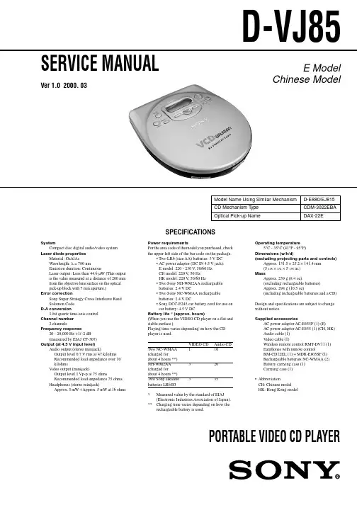
Model Name Using Similar Mechanism D-E880/EJ815CD Mechanism T ype CDM-3022EBA Optical Pick-up NameDAX-22ESERVICE MANUALE Model Chinese ModelD-VJ85PORTABLE VIDEO CD PLAYERSystemCompact disc digital audio/video system Laser diode propertiesMaterial: GaAlAsWavelength: λ = 780 nmEmission duration: ContinuousLaser output: Less than 44.6 µW (This output is the value measured at a distance of 200 mm from the objective lens surface on the optical pick-up block with 7 mm aperture.)Error correctionSony Super Strategy Cross Interleave Reed Solomon Code D-A conversion1-bit quartz time-axis control Channel number2 channelsFrequency response20 - 20,000 Hz +1/–2 dB (measured by EIAJ CP-307)Output (at 4.5 V input level)Audio output (stereo minijack)Output level 0.7 V rms at 47 kilohms Recommended load impedance over 10kilohmsVideo output (minijack)Output level 1 Vp-p at 75 ohmsRecommended load impedance 75 ohms Headphones (stereo minijack)Approx. 5 mW + Approx. 5 mW at 16 ohmsSPECIFICATIONSPower requirementsFor the area code of the model you purchased, check the upper left side of the bar code on the package.•Two LR6 (size AA) batteries: 3 V DC •AC power adaptor (DC IN 4.5 V jack):E model: 220 - 230 V , 50/60 Hz CH model: 220 V , 50 Hz HK model: 220 V , 50/60 Hz•Two Sony NH-WM2AA rechargeable batteries: 2.4 V DC•Two Sony NC-WMAA rechargeable batteries: 2.4 V DC•Sony DCC-E245 car battery cord for use on car battery: 4.5 V DCBattery life * (approx. hours)(When you use the VIDEO CD player on a flat and stable surface.)Playing time varies depending on how the CD player is used.VIDEO CD Audio CD Two NC-WMAA 110(charged forabout 4 hours **)NH-WM2AA 320(charged forabout 4 hours **)Two Sony alkaline 335batteries LR6SG *Measured value by the standard of EIAJ (Electronic Industries Association of Japan).**Charging time varies depending on how the rechargeable battery is used.Operating temperature5°C - 35°C (41°F - 95°F)Dimensions (w/h/d)(excluding projecting parts and controls)Approx. 131.5 × 25.2 × 141.4 mm (5 1/8 × 3/4 × 5 1/8 in.)MassApprox. 239 g (8.4 oz)(excluding rechargeable batteries)Approx. 298 g (10.5 oz)(including rechargeable batteries and a CD)Design and specifications are subject to change without notice.Supplied accessoriesAC power adaptor AC-E455F (1) (E)AC power adaptor AC-E455 (1) (CH, HK)Audio cable (1)Video cable (1)Wireless remote control RMT-DV11 (1)Earphones with remote controlRM-CD12EL (1) + MDR-E805SP (1)Rechargeable batteries NC-WMAA (2)Battery carrying case (1)Carrying case (1)•AbbreviationCH: Chinese model HK: Hong Kong modelVer 1.0 2000. 03CAUTIONUse of controls or adjustments or performance of proce-dures other than those specified herein may result in haz-ardous radiation exposure.Flexible Circuit Board Repairing•Keep the temperature of the soldering iron around 270°C during repairing.•Do not touch the soldering iron on the same conductor of the circuit board (within 3 times).•Be careful not to apply force on the conductor when soldering or unsoldering.Notes on Chip Component Replacement •Never reuse a disconnected chip component.•Notice that the minus side of a tantalum capacitor may be damaged by heat.This Compact Disc player is classified as a CLASS 1LASER product.The CLASS 1 LASERPRODUCT table is located on the bottom exterior.SAFETY-RELATED COMPONENT WARNING!!COMPONENTS IDENTIFIED BY MARK 0 OR DOTTED LINE WITH MARK 0 ON THE SCHEMATIC DIAGRAMS AND IN THE PARTS LIST ARE CRITICAL TO SAFE OPERATION.REPLACE THESE COMPONENTS WITH SONY PARTS WHOSE PART NUMBERS APPEAR AS SHOWN IN THIS MANUAL OR IN SUPPLEMENTS PUBLISHED BY SONY.NOTES ON HANDLING THE OPTICAL PICK-UP BLOCK OR BASE UNITThe laser diode in the optical pick-up block may suffer electro-static breakdown because of the potential difference generated by the charged electrostatic load, etc. on clothing and the human body.During repair, pay attention to electrostatic breakdown and also use the procedure in the printed matter which is included in the repair parts.The flexible board is easily damaged and should be handled with care.Precautions for Checking Emission of Laser DiodeLaser light of the equipment is focused by the object lens in the optical pick-up so that the light focuses on the reflection surface of the disc. Therefore, be sure to keep your eyes more then 30 cm apart from the object lens when you check the emission of laser diode.Before Replacing the Optical Pick-Up BlockPlease be sure to check throughly the parameters as par the “Opti-cal Pick-Up Block Checking Procedures” (Part No.: 9-960-027-11) issued separately before replacing the optical pick-up block.Note and specifications required to check are given below.•FOK output : IC601 eg pinWhen checking FOK, remove the lead wire to disc motor.•RF signal P-to-P value : 0.35 - 0.65 Vp-pLaser Diode Checking MethodsDuring normal operation of the equipment, emission of the laser diode is prohibited unless the upper lid is closed while turning ON the S801. (push switch type)The following two checking methods for the laser diode are operable.•Method:Emission of the laser diode is visually checked.1.Open the upper lid.2.With a disc not set, turn on the S801 with a screwdriver having a thin tip as shown in Fig.1.or TAP802 is shorted as shown in Fig.2.Note:Do not push the detection lever strongly, or it may be bentor damaged.3.Press the u button.4.Observing the objective lens, check that the laser diode emits light.When the laser diode does not emit light, automatic power control circuit or optical pickup is faulty.In this operation, the objective lens will move up and down 5times along with inward motion for the focus search.Fig. 1TABLE OF CONTENTS1. GENERALGetting started (4)Playing a VIDEO CD (4)Playing an audio CD (5)2. DISASSEMBLY2-1. Cabinet (Lower) Assy (6)2-2. Lid Assy, Upper (6)2-3. Switch Board (7)2-4. MD Assy (7)2-5. Main Board, IR Board (8)2-6. Optical Pick-up (8)3. TEST MODE3-1. How to Enter the Test Mode (9)3-2. How to Release the Test Mode (9)3-3. Each Key Function in Test Mode (9)4. ELECTRICAL ADJUSTMENT4-1. Focus Bias Check (11)5. DIAGRAMS5-1. IC Pin Descriptions (12)5-2. Block Diagram –CD Section (1/2)– (17)5-3. Block Diagram –CD Section (2/2)– (19)5-4. Block Diagram –Video Section– (21)5-5. Block Diagram –Power Supply Section– (23)5-6. Printed Wiring Boards (25)5-7. Schematic Diagram –Main Section (1/4)– (29)5-8. Schematic Diagram –Main Section (2/4)– (31)5-9. Schematic Diagram –Main Section (3/4)– (33)5-10. Schematic Diagram –Main Section (4/4)– (35)6. EXPLODED VIEWS6-1. Cabinet Section (41)6-2. CD Mechanism Deck Section (42)7. ELECTRICAL PARTS LIST (43)SECTION 1GENERALThis section is extracted from instruction manual.Locating the ControlsFor details, see pages in parentheses.CD player (front)Getting startedRemote controlNoteUse only the supplied remote control. You cannot operate this VIDEO CD player with the remote control supplied with other VIDEO CD players.(Front)(Rear)clip.CD player (rear)Wireless remote controlmodel.21, 22, 23)(Continued)Playing a VIDEO CDYou can play back a VIDEO CD, using the supplied AC power adaptor. You can also use rechargeable batteries and alkaline batteries. (See “Connecting a power source ” on pages 28 –30.)To produce color pictures normally, you need to set the color system properly according to theDo this Press u .Press x /CHG (x ).Press uPress > repeatedly until you find the scene or track.Press . repeatedly unitl you find the scene or track.Press the number button of the track (wireless remote control only).Press . or > and hold it down until m or M appears on the TV screen.To Pause StopResume play after pauseLocate the next or succeeding tracks Locate the current or preceding tracks Locate a specific track directlyLocate a point in the track while monitoring the picture**To return to normal playback, press u .The above operations can also be done with the buttons on the supplied earphones with remote control or wireless remote control.About the display•No indication appears on the display while you operate the unit with the wired remote control.•During play, the track number and the elapsed playing time of the current track appear.•During pause, the elapsed playing time flashes.If the volume level does not increase (when listening with the headphones/earphone)Is A VLS set to “LIMIT ”? Set A VLS to “NORM.” For details, see “To protect your hearing (A VLS)” on page 24.If a cable is connected to the AUDIO OUT jack, you cannot adjust the volume. In such a case,disconnect the cable.Removing the VIDEO CDPlaying an audio CDYou can also use rechargeable batteries, alkaline batteries and a car battery. (See “Connecting aheard.Press ux /CHG (x )u. once**. repeatedly**> once**> repeatedly**Number buttons of the track (wireless remote control only)**Hold down >**Hold down .**To Pause StopResume play after pauseFind the beginning of the current track (AMS*)Find the beginning of previous tracks (AMS)Find the beginning of the next track (AMS)Find the beginning of succeeding tracks (AMS)Locate a specific track directly Go forward quickly Go backwards quickly *Automatic Music Sensor**These operations are possible during both play and pause.The above operations can also be done with the buttons on the supplied earphones with remote control or wireless remote control.If you press REPEAT/ENTER (RPT/ENT) to display “REPEAT ”, you can locate the tracks continuously in the following order:•When using >: next track t next track ...... last track t first track t second track ......•When using .: previous track t previous track ...... first track t last track ......About the display•When playing an audio CD using the AC power adaptor, indications on the remote controldisplay window go off until the sound is heard.•When you press u , the total number of tracks in the audio CD and total playing time appear for about two seconds.•During play, the track number and the elapsed playing time of the current track appear.•Between tracks, the time to the beginning of the next track appears with the “-” indication.•During pause, the elapsed playing time flashes.If the volume level does not increaseIs A VLS set to “LIMIT ”? Set A VLS to “NORM.” For details, see “To protect your hearing (A VLS)” on page 24.If a cable is connected to the AUDIO OUT jack, you cannot adjust the volume. In such a case,disconnect the cable.Removing the audio CD3 boss2 boss1 screw (M1.4), step4 lid assy, upperlid, battery caseclaws7 claws6 claw4 claws8 CN8013 claws5 claws2 screws (B2)1 screws (B2)9cabinet (lower) assy • The equipment can be removed using the following procedure.2-2. LID ASSY, UPPERSECTION 2DISASSEMBL YNote : Follow the disassembly procedure in the numerical order given.2-1. CABINET (LOWER) ASSYSetCabinet (Lower) AssyLid Assy, Upper Switch BoardMain Board, IR Board Optical Pick-up4SWITCH board2-3. SWITCH BOARD 2-4. MD ASSY36 optical pick-up2 rack1 M1.4x1.83 M1.4x45 shaft, standard4 bracket assy, sled2-5. MAIN BOARD, IR BOARD2-6. OPTICAL PICK-UPSECTION 3TEST MODE3-1. OUTLINEThis set has the test mode in which the pick-up can be operational checked and the video signal can be verified.3-2. PICK-UP OPERATIONAL CHECKS3-2-1. Setting the test mode 1.Switch positionsOPEN switch (S801): OPEN HOLD switch (S804): OFF A VLS switch (S893): OFF2.Short the TEST terminal TAP801 (TEST) by soldering it.Remove the solder from the TAP901 (V-TEST) and open the terminal.3.Supply4.5 V DC from the DC jack (J401).3-2-2. Releasing the test mode1.Open the TEST terminal TAP801 (TEST) and short the TAP901 (V-TEST).2.Turn the power OFF.3-2-3.Operational checks1.When a specific key is operated:KEYContents of the operation.((LCD DISPLAY))u Spindle on. Tracking servo off.((UP 00 03))x All servo off. Mute on.CHG ((10 different displays are repeatedly presented.))Moves the pick-up to the outside (with the open >switch open). Tracking servo off. Mute on.NEXT((Among 10 different displays, the display when the key is pressed is held.))Moves the pick-up to the inside (with the open.switch open). Tracking servo off. Mute on.PREV((Among 10 different displays, the display when the key is pressed is held.))2.In play mode • Press the u key:KEYContents of the operation.((LCD DISPLAY))Tracking servo on. Mute off.Each time this key is pressed, the display changes PLAY as follows:MODEx1 speed t x2 speed t x3 speed t x4 speed t x1 speed(( 01 00 01)) t ((02 00 02)) t ((03 00 03))t ((04 00 04))Each time this key is pressed, the display changes SELECT as follows:REPEAT/Tracking gain up. Emphasis on. LCD back light ENTERon h Tracking gain down. Emphasis off.LCD back light off3-3. VIDEO SIGNAL VERIFICATION3-3-1. Setting the test mode 1.Switch positionsOPEN switch (S801): OPEN HOLD switch (S804): OFF A VLS switch (S893): OFF2.Short the TEST terminal TAP801(TEST) by soldering it.Remove the solder from the TAP901(V-TEST) and connect the terminal to the TP945 (VDD) with a 47 k Ω resistor.3.Supply 4.5V DC from the DC jack (J401).3-3-2. Releasing the test mode1.Open the TEST terminal TAP801(TEST). Remove the resistor from the TAP901 (V-TEST) and short the terminal by soldering it.2.Turn the power OFF.3-3-3. Operational checks1.Connect the TP931 to the TP945 (VDD) with a 47 k Ω resistor (NTSC mode).2.Press the O RETURN key once.3.Verify that a 100% white pattern is output from the VIDEO OUT (J901).4.Press the O RETURN key once (output off).5.Connect the TP931 to the TP919 (GND) (PAL mode).6.Press O RETURN key once.7.Verify that a 100% white pattern is output from the VIDEO OUT (J901).8.Press the O RETURN key once (output off).9.Open the TP931.Fig. 100% white patternAdjustment Location: See page 10.Test Points:– main board (side A) –– main board (side B) –1. 2. 3. 4.5.•SECTION 4 ELECTRICAL ADJUSTMENTCD section adjustments are done automatically in this set.1.2.3.A•Test Points:– 11 –SECTION 5DIAGRAMS5-1. IC PIN DESCRIPTIONS• IC801 TMP88CM22F (SYSTEM CONTROLLER)Pin No.Pin Name I/O Pin Description1VSS I Ground2IRRMC I Infrared remote control signal input3FOKI I Focus OK signal input from CXD3027R (IC601).4AGCCON O AGC control pulse output5XLEDDISP O CHG/HOLD LED control signal output6VCC SWITCHING O Control signal output for Switching power supply circuit.7AMUTE O Analog audio muting ON/OFF signal control signal output (H: Mute ON)8VCC2 ON O VCC2 voltage control output9XRST O Reset signal output to CXD3027R (IC601). (L: Reset)10SCK O Serial data transfer clock signal output to CXD3027R (IC601).11SDTI I Serial data input from CXD3027R (IC601).12SDTO O Serial data output to CXD3027R (IC601).13SLPOUT O WAKE-UP control signal output (for system standby reset)14SEL I Plug-in detection signal input of AUDIO OUT (OPTICAL) jack.15CHGMNT1I Battery charge voltage detection input from TB2119F (IC401).16VCDKEY I VCD key input17BATMNT I Battery voltage detection input18KEY I Key input from switch board (A/D input).19RMKEY I Key input from headphones with remote controller (A/D input).20DCINMNT I DC input voltage detection input (A/D input) DC input jack use/no-use detect input 21OPEN I CD door open/close detection input22VREFL I Reference voltage (0 V) input for A/D converter.23VREFH I Reference voltage (+2 V) input for A/D converter.24VDD—Power supply pin (+2 V)25SCOR I Sub code sync detection input from CXD3027R (IC601).26GRSCOR I GRSCOR signal input27FG I FG pulse input28BEEP O Beep sound output to headphone AMP (IC351).29XU TX REQ O Request signal output to TMP87PM41U (IC902).30RMSCK O Communication clock to CXD751-103R (IC802) and TMP87PM41U (IC902).31RMDATI I Communication data bus input from CXD751-103R (IC802) and TMP87PM41U (IC902).32RMDA TO O Communication data bus output to CXD751-103R (IC802) and TMP87PM41U (IC902).33RMRW O Read/write control signal output to headphones with remote. (L: Read, H: Write) 34RMLAT O Serial data latch pulse output to headphones with remote.35WFCKI I WFCK input36NC—Not used. (Open)37XNTSC I I NTSC/PAL select input (“L”: PAL, “H”: NTSC)38A VLS I A VLS (Automatic V olume Limiter System) switch input (L: Normal, H: Limit) 39HOLD I HOLD switch input (L: HOLD on, H: HOLD off)40EX BATT I EXT BATT plug-in detection input41XSPDOE O Spindle motor driver control signal output42XHGON O Optical pick-up VCC control signal output (L: on)43XLAT O Serial data latch pulse output to CXD3027R (IC601). (for ESP)44XSOE O Output enable signal output (for ESP)45DRVLT O Spindle motor driver latch output46XPOWLT O Latch output to VCD control IC.47XDOUTON O DIGITAL OUT LED control signal output48XAPC OFF O APC mute signal output (L: mute)49XVRST O Reset signal output to TMP87PM41U (IC902).50 – 52SEG14 – 12O LCD drive segment output53 – 56SEG11 – 8O LCD drive segment output– 12 –Pin No.Pin Name I/O Pin Description57 – 64SEG7 – 0O LCD drive segment output65 – 68COM3 – 0O LCD drive common output69 – 71V3 – 1O LCD drive bias output72, 73C1, 0O Capacitor connected terminal of LCD driver for voltage-up.74STOP O Stop signal output to VCD control IC.75TEST I Test terminal for IC. (Fixed at L in this set)76XHPSW O Headphone AMP ON/OFF control signal output (L: ON) 77XLIGHT O LCD back light control signal output to LCD.78RESET I System reset signal input from TB2119F (IC401). (L: Reset) 79XIN I Oscillation input80XOUT O Oscillation output (Open)– 13 –• IC902 TMP87PM41U (MICON VIDEO ENCODER/VIDEO CONTROLLER)Pin No.Pin Name I/O Pin Description1 – 8P00 – 07—Not used. (Open)9(INT0) P10—Not used. (Open)10(INT1) P11—Not used. (Open)11(INT2/TC1) P12—Not used. (Open)12(DVO) P13—Not used. (Open)13(PPG) P14—Not used. (Open)14(TC2) P15—Not used. (Open)15P16—Not used. (Open)16P17I Visual system test mode pin (“L”: Test mode)17P20 (INT5/STOP)I Interruption request signal input from CL680T-D1 (IC906).18TEST I Test pin (Fixed at “L” in this set)19P21 (XTI)—Not used. (Open)20P22 (XTOUT)—Not used. (Open)21RESET I I System reset signal input from TMP88CM22F (IC801). (“L”: Reset) 22XIN I I High frequency oscillator input from TMP88CM22F (IC801).23XOUT O High frequency oscillator output (Not used in this set)24VSS—Digital ground25P30O CD DA/CD ROM judgment output (“L”: Audio CD)26 – 30P31 – 35—Not used. (Open)31——Not used. (Open)32 C RESET O Reset signal output to CL680T-D1 (IC906). (“L”: Reset)33P40O Ready signal output to CL680T-D1 (IC906).34P41O Address select signal output to CL680T-D1 (IC906).35P42 (SCK1)O Serial clock signal output to CL680T-D1 (IC906).36P43 (SI1)I Serial data signal input from CL680T-D1 (IC906).37P44 (SO1)O Serial data signal output to CL680T-D1 (IC906).38P45 (SCK2)I Serial clock signal input from TMP88CM22F (IC801).39P46 (SI2)I Serial data signal input from TMP88CM22F (IC801).40P47 (SO2)O Serial data signal output to TMP88CM22F (IC801).41P50 (INT3/TC3)I Request signal input from TMP88CM22F (IC801).42P51 (INT4/TC4)I Ready signal input from TMP88CM22F (IC801).43P52 (PWM/PDO)O Request signal output to TMP88CM22F (IC801).44P53 (HPWM0)—Not used. (Open)45P54 (HPWM1)—Not used. (Open)46A VSS—Not used. (Open)47A VREF—Not used. (Open)48(AIN0) P60—Not used. (Open)49(AIN1) P61—Not used. (Open)50(AIN2) P62—Not used. (Open)51(AIN3) P63—Not used. (Open)52(AIN4) P64—Not used. (Open)53(AIN5) P65—Not used. (Open)54(AIN6) P66—Not used. (Open)55(AIN7) P67—Not used. (Open)56VDD—Digital power supply pin (+3.2 V)57(AIN10) P70—Not used. (Open)58(AIN11) P71—Not used. (Open)59(AIN12) P72—Not used. (Open)60(AIN13) P73—Not used. (Open)61(AIN14) P74—Not used. (Open)62(AIN15) P75—Not used. (Open)63(AIN16) P76—Not used. (Open)64(AIN17) P77—Not used. (Open)– 14 –– 39 –IC601 CXD3027RA9A8A7DVSS V D D C O U M I R D F C F O P W M L O C H P H P H P V D D C 17M D M D S S T S F D S R D T F D T R D F F D F R D V S S T E S T E S A V D D I G E A V S S R F D O E C A S 2301W E R A S 1110V D D 0123V D D 2O U T 2I N 2O U T 2V S S 2V S S 1O U T 1I N 1O U T 1V D D 1V S S T A O T A I V D D C K IA6A5A4XWRE XRDE XEMP XWIH XQOK AMUTE SDTI XQCK SCSY SCOR VSS0SBSO EXCK XRST SYSM SDTO XLAT CLOK SENS SCLK XSOE ATSK R4MBCK PCMDI PCMD LRCKI LRCK DOUT VDD2WFCK C2PO GFS XPCK XUGF WDCK VSS2XTSL AVDD3ASYO ASYI BIAS RFAC AVSS3CLTV PCO FILI FILO VCTL VPCO VC A B– 40 –IC351 TA2120FNBEEP NFOUTSWGNDOUTINDETATT MT MT PW BIASBST BST IC802 CXD751-103RIC803 TC7W53FU (TE12R)O 26O 27C C S S 2S B W S E L 2S E L 2V S S X L T S O S C K R E S E L 2L T– 41 –SECTION 6EXPLODED VIEWSRef. No.Part No.DescriptionRemark6-1. CABINET SECTIONRef. No.Part No.DescriptionRemarkNOTE:•The mechanical parts with no referencenumber in the exploded views are not supplied.•Accessories and packing materials are given in the last of this parts list.•Items marked “*” are not stocked sincethey are seldom required for routine service.Some delay should be anticipated when ordering these items.The components identified by mark 0 or dotted line with mark 0 are critical for safety.Replace only with part number specified.1X-4952-439-1CABINET (LOWER) SUB ASSY 24-225-414-01LID, BATTERY CASE 34-908-792-91SCREW (B2)44-224-048-01FOOT, RUBBER54-225-413-01WINDOW (RAY CATCHER)64-224-020-01KNOB (HOLD)*71-676-499-11IR BOARD8A-3323-414-A MAIN BOARD, COMPLETE94-225-416-01TERMINAL SPRING (–), BATTERY 104-225-417-01PLATE, CHARGE DETECTION 114-225-415-01TERMINAL BOARD (+), BATTERY 124-908-792-51SCREW (B2)133-318-382-01SCREW (1.7X3), TAPPING 144-225-407-01LEVER, DETECTION 154-224-229-01SPACER (A)16X-4952-438-1OPEN ASSY 174-224-016-01KNOB (OPEN)184-224-015-01BUTTON (VOL)19X-4952-437-1CABINET (UPPER) SUB ASSY 20X-4952-436-1PLATE ASSY, ORNAMENTAL 213-345-710-21SCREW (M1.4X3) TAPPING 22X-4952-435-1LID SUB ASSY, UPPER 234-224-230-01SPACER (B)243-043-558-01SPRING (B) (OPEN)25X-4952-205-1ARM ASSY, SWITCHING *261-674-587-21SWITCH BOARD274-224-053-01SCREW (M1.4), STEP 284-221-927-01INSULATOR293-375-114-51SCREW303-042-766-11CUSHION (BATT)313-318-201-51SCREW (B) (1.4X4), TAPPING 323-318-382-01SCREW (1.7X3), TAPPING 333-045-650-01SHEET, RADIATION343-044-559-01RAIL354-225-396-01SPACER (C)*361-678-339-11WAKE BOARD– 42 –51525354555657575859606162636465M902M9016-2. CD MECHANISM DECK SECTION(CDM-3022EBA)Ref. No.Part No.DescriptionRemark Ref. No.Part No.DescriptionRemark51A-3328-418-A CHASSIS ASSY (INCLUDING M902)524-220-645-01SHAFT, STANDARD 053X-4952-079-1DAX-22E RP ASSY 544-220-646-01RACK553-704-197-92SCREW (M1.4X1.8), LOCKING56X-4951-687-1BASE ASSY, SLED573-348-998-61SCREW (M1.4X4), TAPPING, PAN584-220-648-01GEAR (C)593-338-645-31WASHER (0.8-2.5)60A-3328-298-A SCREW ASSY, FEED61A-3328-299-AMOTOR BLOCK ASSY , SLED(INCLUDING M901)624-964-564-01SCREW (M1.2X1.6)633-686-458-03SCREW (P1.4X3.5), TAPPING 644-973-631-31SCREW65X-4951-688-1BRACKET ASSY , SLEDThe components identified by mark 0 or dotted line with mark 0 are critical for safety.Replace only with part number specified.– 43 –SECTION 7ELECTRICAL PARTS LISTRef. No.Part No.Description Remark Ref. No.Part No.Description Remark NOTE:•Due to standardization, replacements in the parts list may be different from the parts specified in the diagrams or the components used on the set.•RESISTORSAll resistors are in ohms.METAL:Metal-film resistor.METAL OXIDE: Metal oxide-film resistor.F:nonflammable •Items marked “*” are not stocked sincethey are seldom required for routine service.Some delay should be anticipated when ordering these items.•SEMICONDUCTORSIn each case, u : µ, for example:uA..: µA..uPA..: µPA..uPB..: µPB..uPC..: µPC.. uPD.. : µPD..•CAPACITORS uF : µF •COILS uH : µHThe components identified by mark 0 or dotted line with mark 0 are critical for safety.Replace only with part number specified.When indicating parts by reference number, please include the board.MAIN•AbbreviationCH : Chinese model HK : Hong Kong modelIR*1-676-499-11IR BOARD*********< IC >PH9018-749-015-96IC GP1UC10J*************************************************************A-3323-414-A MAIN BOARD, COMPLETE*********************< CAPACITOR >C1011-104-851-11TANTAL. CHIP 10uF 20%10V C1021-162-925-11CERAMIC CHIP 68PF 5%50V C1031-164-230-11CERAMIC CHIP 220PF 5%50V C1041-126-246-11ELECT CHIP 220uF 20%4V C1611-107-826-11CERAMIC CHIP 0.1uF 10%16V C1631-125-838-11CERAMIC CHIP 2.2uF 10% 6.3V C2011-104-851-11TANTAL. CHIP 10uF 20%10V C2021-162-925-11CERAMIC CHIP 68PF 5%50V C2031-164-230-11CERAMIC CHIP 220PF 5%50V C2041-126-246-11ELECT CHIP 220uF 20%4V C2611-107-826-11CERAMIC CHIP 0.1uF 10%16V C2631-125-838-11CERAMIC CHIP 2.2uF 10%6.3V C3011-117-720-11CERAMIC CHIP 4.7uF 10V C3041-164-156-11CERAMIC CHIP 0.1uF 25V C3061-115-156-11CERAMIC CHIP 1uF 10V C3071-127-569-11TANTAL. CHIP 100uF 20%4V C3081-164-156-11CERAMIC CHIP 0.1uF 25V C3611-135-259-11TANTAL. CHIP 10uF 20% 6.3V C3621-115-156-11CERAMIC CHIP 1uF 10V C3631-125-837-11CERAMIC CHIP 1uF 10%6.3V C3641-115-156-11CERAMIC CHIP 1uF 10V C3651-135-259-11TANTAL. CHIP 10uF 20% 6.3V C4011-164-156-11CERAMIC CHIP 0.1uF 25V C4031-162-964-11CERAMIC CHIP 0.001uF 10%50V C4041-104-752-11TANTAL. CHIP 33uF 20% 6.3V C4051-104-752-11TANTAL. CHIP 33uF 20% 6.3V C4061-164-156-11CERAMIC CHIP 0.1uF 25V C4071-162-970-11CERAMIC CHIP 0.01uF 10%25V C4081-109-982-11CERAMIC CHIP 1uF 10%10V C4111-109-982-11CERAMIC CHIP 1uF 10%10V C4121-162-970-11CERAMIC CHIP 0.01uF 10%25V C4131-162-925-11CERAMIC CHIP 68PF 5%50V C4141-125-899-11TANTAL. CHIP 220uF 20%4V C4151-110-569-11TANTAL. CHIP47uF20%4VC4161-115-156-11CERAMIC CHIP 1uF 10V C4171-104-852-11TANTAL. CHIP 22uF 20%10V C4181-164-156-11CERAMIC CHIP 0.1uF 25V C4191-104-847-11TANTAL. CHIP 22uF 20%4V C4201-115-156-11CERAMIC CHIP 1uF 10V C4211-164-677-11CERAMIC CHIP 0.033uF 10%16V C4221-162-927-11CERAMIC CHIP 100PF 5%50V C4231-162-970-11CERAMIC CHIP 0.01uF 10%25V C4241-110-569-11TANTAL. CHIP 47uF 20%6.3V C4251-164-156-11CERAMIC CHIP 0.1uF 25V C4261-104-851-11TANTAL. CHIP 10uF 20%10V C4271-115-156-11CERAMIC CHIP 1uF 10%10V C4281-164-156-11CERAMIC CHIP 0.1uF 25V C4301-135-201-11TANTALUM CHIP 10uF 20%4V C4311-110-569-11TANTAL. CHIP 47uF 20%4V C4321-113-682-11TANTAL. CHIP 33uF 20%10V C4331-164-156-11CERAMIC CHIP 0.1uF 25V C4341-162-970-11CERAMIC CHIP 0.01uF 10%25V C4351-125-838-11CERAMIC CHIP 2.2uF 10% 6.3V C4361-110-501-11CERAMIC CHIP 0.33uF 10%16V C4371-109-982-11CERAMIC CHIP 1uF 10%10V C4381-115-156-11CERAMIC CHIP 1uF 10V C4391-110-569-11TANTAL. CHIP 47uF 20%4V C4411-162-970-11CERAMIC CHIP 0.01uF 10%25V C4421-162-970-11CERAMIC CHIP 0.01uF 10%25V C4441-115-467-11CERAMIC CHIP 0.22uF 10%10V C4451-104-913-11TANTAL. CHIP 10uF 20%16V C4461-164-156-11CERAMIC CHIP 0.1uF 25V C4471-109-982-11CERAMIC CHIP 1uF 10%10V C4481-162-925-11CERAMIC CHIP 68PF 5%50V C4491-115-566-11CERAMIC CHIP 4.7uF 10%10V C4501-125-838-11CERAMIC CHIP 2.2uF 10% 6.3V C4511-162-964-11CERAMIC CHIP 0.001uF 10%50V C4521-162-964-11CERAMIC CHIP 0.001uF 10%50V C4531-162-964-11CERAMIC CHIP 0.001uF 10%50V C4541-162-969-11CERAMIC CHIP 0.0068uF 10%25V C4561-115-156-11CERAMIC CHIP 1uF 10%10V C4571-162-964-11CERAMIC CHIP 0.001uF 10%50V C4591-110-569-11TANTAL. CHIP 47uF 20% 6.3V C4611-162-962-11CERAMIC CHIP 470PF10%50V C4621-162-968-11CERAMIC CHIP 0.0047uF 10%50V C4631-107-826-11CERAMIC CHIP 0.1uF 10%16V C5011-164-156-11CERAMIC CHIP 0.1uF 25V C5021-104-847-11TANTAL. CHIP 22uF 20%4V C6011-164-156-11CERAMIC CHIP0.1uF25V。