
BIT1612_MasterMode20090519
- 格式:pdf
- 大小:284.58 KB
- 文档页数:24

利用BIOS-ID获得主板的信息
以下是AMI的BIOS-ID,,同时也会逐步加入新的代码的。
在计算机启动,进行设备自检时,按下PAUSE键暂停,这时屏幕左下端的一段字符串就是我们所说的BIOS-ID。
AMI和AWARD是两家最著名的BIOS厂家。虽说目前大多主板都采用AWARD公司的BIOS,但是也有不少主板厂商采用AMI的BIOS,例如,大家都知道的、以生产TXPRO、VXPRO系列主板而出名的香港明致公司(PCCHIPS)。在很多人眼里,明致公司的产品是质优价廉的同义词,著名的宏鹰主板,麒麟主板等等,实际上都是明致公司的产品,它们采用的BIOS大部分都是AMI公司的。很多朋友,尤其是当初攒机时追求低价位的朋友,使用的是明致公司的主板产品;采用的是AMI公司的BIOS。这些朋友在升级时同样也遇到了如何准确识别主板型号的问题,在升级BIOS之前同样需要知道主板的详细资料。
一、在采用AMI公司BIOS的主板上,如何获得BIOS号码。
同采用AWARD BIOS的主板一样,采用AMI BIOS的电脑启动到自检内存时,BIOS号码也会在屏幕的最下面一行显示出来,其格式大约是:
51-0119-001107-00111111-071595-82437FX-H
您的主板身份就隐藏在上述的信息中。这时,您可以按下键盘上的PAUSE键把这些信息抄下来,以供仔细研究。很多朋友向我抱怨,“按下PAUSE键后,机器暂停的时间太短;来不及抄下BIOS号码,机器就接着启动了”。您先不用着急,我下面就向您介绍另外一个办法;使用该办法,您即使将屏幕上显示的所有内容都仔细地抄下来也都会有足够的时间。方法就是:
按着键盘上的某个按键,然后打开电脑的电源开关;电脑在启动的过程中,自检到了键盘错误就会停止继续引导,直到您按F1键。这时您就可以随心所欲地抄下BIOS信息了。当然,您也可以干脆将键盘从电脑中拔下来,然后开机;电脑启动后,自检到键盘错误停下来后,您就可以有充足的时间来抄写主板的BIOS号码了。

C51 Manchester译码源程序 C51曼彻斯特码译码源程序
2009-04-30 11:14
/*
manchester编码方式:0为10 1为01,如果与其相反则需要做相应的修改。
适用于125KHz非接触式ID卡,EM4100兼容格式ID卡(64bits, Manchester编码)
MCU:stc12c54xx
crystal:11.0592M
使用资源:外部中断0(INT0)+PCA0
*/
#include
#include
#include
#define Channe256uS_H 0x00 //模块60mS 定时常数高位
#define Channe256uS_L 0xEC //模块60mS 定时常数低位
#define uint8 unsigned char
sbit RFID_DATA = P3^2; //外部中断口 接收数据
/*/函数申明 */
void start_Read() ;
void Data_reveice() ;
void Lmove_bite() ;
uint8 find_head() ;
uint8 Data_L_check() ;
uint8 Data_R_check() ;
void get_data();
uint8 Data_Sever() ;
void Get_EffectData(uint8 edata) ;
void Init_PCA0();
void DAT_Change(uint8 dat[]);
void init_dev(void);
uint8 tcount ;// 定时中断计数
uint8 count ;//接收数据位数计数
uint8 t_count ;//获得数据及校验变量。
uint8 temp ;// 临时变量
uint8 temp_buf[16] ;//128个Machester位 55个数据位 缓冲区。
欧姆龙 PLC通信协议
参考: W342 --SYSMAC CS/CJ Series Communications Commands
欧姆龙通信命令可分为两类:
1: C-mode commands 只可通过串口通讯 2: FINS commands 既可通过串口通讯也可通过各类网络通信(适应性较强)
面只讲 FINS命令
一、命令发送:
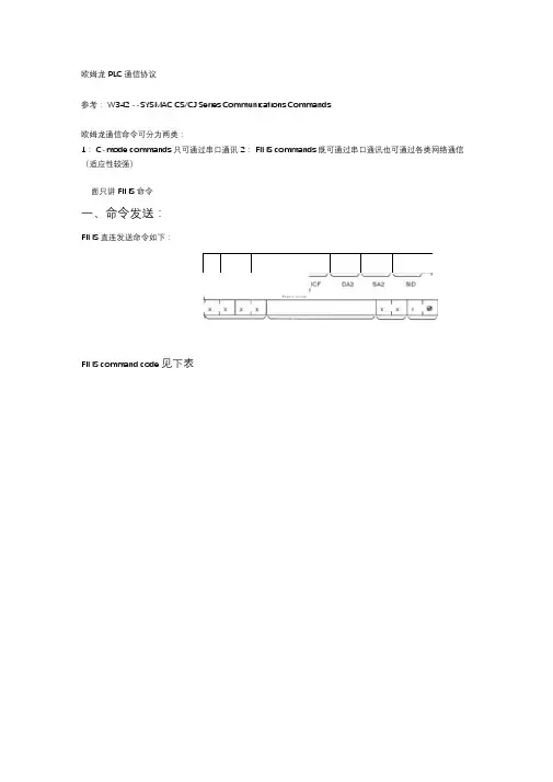
FINS直连发送命令如下:
FINS command code 见下表
5-1-1 FINS COmmandS
Thefdlwirg table IlStS the FINS CCXnmands.
HPe COmmDnd cod∙ NAme FUnCtiOn
MR SR
VQ f∏∙fτory ar∞
CECe33 01 01 MEMORY AREA READ Rood。the ContOnt・ Of COnoOCU⅛v∙
l,0 Rvmoryarca ・orcs・
01 0? NFMOR、ARFA WRrF (Sm nct
mβπwyarea worcs.
01 03 MEMOR、AREA FllL (See note) WriteS Ihesamedats to tne SOeCried
ranςeof IQ menoryarea W(Xd5.
01 CM MULTlPLE MEMORr AREA READ ReaaS tħeconte∩U Of SPeQfied nor-
consecutive I/O InerTOry area^oras.
01 05 MCMORY AREA T□ANSΓER (See rotσ.∣ Copes f>e COrtCnto Of GCnOeCKXKe /O
∣∏σmcryafea ∙CTGB IoarxXbrf VO
meπχχy 孔 乱
ParAmotQravQa 0∞C33 CQ 01 FARAMETER APEA PEAD ∏βadβ the COntOnCf ConCOCUftVo pare
1.General descriptionThe LPC2109/2119/2129 are based on a 16/32-bit ARM7TDMI-S CPU with real-timeemulation and embedded trace support, together with 64/128/256 kB of embeddedhigh-speed flash memory. A 128-bit wide memory interface and a unique acceleratorarchitecture enable 32-bit code execution at maximum clock rate. For critical code sizeapplications, the alternative 16-bit Thumb mode reduces code by more than 30% withminimal performance penalty.With their compact 64-pin package, low power consumption, various 32-bit timers,4-channel 10-bit ADC, two advanced CAN channels, PWM channels and 46 fast GPIOlineswithuptonineexternalinterruptpinsthesemicrocontrollersareparticularlysuitablefor automotive and industrial control applications, as well as medical systems andfault-tolerant maintenance buses. With a wide range of additional serial communicationsinterfaces, they are also suited for communication gateways and protocol converters aswell as many other general-purpose applications.Remark:Throughout the data sheet, the termLPC2109/2119/2129 will apply to deviceswith and without the /00 or /01 suffixes. The /00 or the /01 suffix will be used todifferentiate from other devices only when necessary.2.Features2.1Key features brought by LPC2109/2119/2129/01 devicesIFastGPIOportsenableportpintogglingupto3.5timesfasterthantheoriginaldevice.They also allow for a port pin to be read at any time regardless of its function.IDedicated result registers for ADC(s) reduce interrupt overhead. The ADC pads are5V tolerant when configured for digital I/O function(s).IUART0/1 include fractional baud rate generator, auto-bauding capabilities andhandshake flow-control fully implemented in hardware.IBuffered SSP serial controller supporting SPI, 4-wire SSI, and Microwire formats.ISPI programmable data length and master mode enhancement.IDiversified Code Read Protection (CRP) enables different security levels to beimplemented. This feature is available in LPC2109/2119/2129/00 devices as well.IGeneral purpose timers can operate as external event counters.2.2Key features common for all devicesI16/32-bit ARM7TDMI-S microcontroller in a tiny LQFP64 package.I8/16kB on-chip static RAM.LPC2109/2119/2129Single-chip16/32-bitmicrocontrollers;64/128/256kBISP/IAP