IRLML2803
- 格式:pdf
- 大小:190.59 KB
- 文档页数:9
IRLML2803
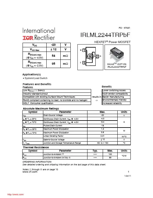
Fifth Generation HEXFETs from International Rectifierutilize advanced processing techniques to achieveextremely low on-resistance per silicon area. This benefit,combined with the fast switching speed and ruggedizeddevice design that HEXFET Power MOSFETs are wellknown for, provides the designer with an extremely efficientand reliable device for use in a wide variety of applications.A customized leadframe has been incorporated into thestandard SOT-23 package to produce a HEXFET PowerMOSFET with the industry's smallest footprint. Thispackage, dubbed the Micro3, is ideal for applicationswhere printed circuit board space is at a premium. The lowprofile (<1.1mm) of the Micro3 allows it to fit easily intoextremely thin application environments such as portable
electronics and PCMCIA cards.VDSS = 30VRDS(on) = 0.25ΩHEXFET® Power MOSFET
Description
4/28/03lGeneration V TechnologylUltra Low On-ResistancelN-Channel MOSFETlSOT-23 FootprintlLow Profile (<1.1mm)lAvailable in Tape and ReellFast SwitchingSDG
Micro3Parameter Max. UnitsID @ TA = 25°CContinuous Drain Current, VGS @ 10V1.2ID @ TA = 70°CContinuous Drain Current, VGS @ 10V0.93 AIDMPulsed Drain Current 7.3PD @TA = 25°CPower Dissipation540 mWLinear Derating Factor4.3 mW/°CVGSGate-to-Source Voltage ± 20 Vdv/dtPeak Diode Recovery dv/dt 5.0 V/nsTJ, TSTGJunction and Storage Temperature Range-55 to + 150 °CAbsolute Maximum Ratings
Parameter Typ.Max.UnitsRθJAMaximum Junction-to-Ambient 230Thermal Resistance°C/WPD - 91258DIRLML2803ParameterMin.Typ.Max.Units ConditionsV(BR)DSSDrain-to-Source Breakdown Voltage30VVGS = 0V, ID = 250µA∆V(BR)DSS/∆TJBreakdown Voltage Temp. Coefficient0.029V/°CReference to 25°C, ID = 1mA0.25VGS = 10V, ID = 0.91A 0.40VGS = 4.5V, ID = 0.46A VGS(th)Gate Threshold Voltage1.0VVDS = VGS, ID = 250µAgfsForward Transconductance0.87SVDS = 10V, ID = 0.46A1.0VDS = 24V, VGS = 0V25VDS = 24V, VGS = 0V, TJ = 125°CGate-to-Source Forward Leakage-100VGS = -20V Gate-to-Source Reverse Leakage100VGS = 20VQgTotal Gate Charge3.35.0ID = 0.91AQgsGate-to-Source Charge0.480.72nCVDS = 24VQgdGate-to-Drain ("Miller") Charge1.11.7VGS = 10V, See Fig. 6 and 9 td(on)Turn-On Delay Time3.9VDD = 15VtrRise Time4.0ID = 0.91Atd(off)Turn-Off Delay Time9.0RG = 6.2ΩtfFall Time1.7RD = 16Ω, See Fig. 10 CissInput Capacitance85VGS = 0VCossOutput Capacitance34pFVDS = 25VCrssReverse Transfer Capacitance15 = 1.0MHz, See Fig. 5ΩµAnAnsIGSSIDSSDrain-to-Source Leakage CurrentRDS(on)Static Drain-to-Source On-ResistanceElectrical Characteristics @ TJ = 25°C (unless otherwise specified)
ParameterMin.Typ.Max.Units ConditionsISContinuous Source CurrentMOSFET symbol(Body Diode)showing theISMPulsed Source Currentintegral reverse(Body Diode) p-n junction diode.VSDDiode Forward Voltage1.2VTJ = 25°C, IS = 0.91A, VGS = 0V trrReverse Recovery Time2640nsTJ = 25°C, IF = 0.91AQrrReverse RecoveryCharge2232nCdi/dt = 100A/µs Source-Drain Ratings and CharacteristicsA7.30.54SDG
Repetitive rating; pulse width limited by max. junction temperature. ( See fig. 11 )ISD ≤ 0.91A, di/dt ≤ 120A/µs, VDD ≤ V(BR)DSS, TJ ≤ 150°CNotes: Pulse width ≤ 300µs; duty cycle ≤ 2%. Surface mounted on FR-4 board, t ≤ 5sec.IRLML2803
Fig 4. Normalized On-ResistanceVs. TemperatureFig 1. Typical Output CharacteristicsFig 2. Typical Output Characteristics
Fig 3. Typical Transfer Characteristics0.1110
0.1110
20µs PULSE WIDTH T = 25°CAJDSV , Drain-to-Source Voltage (V) 3.0V VGS TOP 15V 10V 7.0V 5.5V 4.5V 4.0V 3.5V BOTTOM 3.0VDI , Drain-to-Source Current (A)
0.1110
0.1110
ADSV , Drain-to-Source Voltage (V)DI , Drain-to-Source Current (A)
20µs PULSE WIDTH T = 150°CJ 3.0V VGS TOP 15V 10V 7.0V 5.5V 4.5V 4.0V 3.5V BOTTOM 3.0V
0.00.51.01.52.0
-60-40-20020406080100120140160JT , Junction Temperature (°C)R , Drain-to-Source On Resistance
DS(on)(Normalized) V = 10VGSAI = 0.91AD
0.1110
3.03.54.04.55.05.56.0
6.5T = 25°CT = 150°CJJ
GSV , Gate-to-Source Voltage (V)DI , Drain-to-Source Current (A)
A V = 10V 20µs PULSE WIDTHDSIRLML2803
Fig 7. Typical Source-Drain DiodeForward VoltageFig 5. Typical Capacitance Vs.Drain-to-Source Voltage
Fig 8. Maximum Safe Operating AreaFig 6. Typical Gate Charge Vs.Gate-to-Source Voltage020406080100120140160
110100C, Capacitance (pF)
DSV , Drain-to-Source Voltage (V)AV = 0V, f = 1MHzC = C + C , C SHORTEDC = CC = C + CGSiss gs gd dsrss gdoss ds gdCissCossCrss048121620