
CL9904 300mA稳压IC
- 格式:pdf
- 大小:3.17 MB
- 文档页数:8


Rev 3
October 20051/15
15LM2904
Low Power Dual Operational Amplifier
■Internally frequency compensated
■Large DC voltage gain: 100dB
■Wide bandwidth (unity gain): 1.1MHz
(temperature compensated)
■Very low supply current/op (500µA) essentially
independent of supply voltage
■Low input bias current: 20nA (temperature
compensated)
■Low input offset current: 2nA
■Input common-mode voltage range includes
ground
■Differential input voltage range equal to the
power supply voltage
■Large output voltage swing 0V to (V
CC - 1.5V)
Description
This circuit consists of two independent, high
gain, internally frequency compensated which
were designed specifically for automotive and
industrial control system. It operates from a single
power supply over a wide range of voltages. The
low power supply drain is independent of the
magnitude of the power supply voltage.

型 号参 数型 号
2SC1000SI-N 55V 0.1A 0.2W 80MHz2SC982
2SC1008SI-N 80V 0.7A 0.8W 75MHz2SC1012A
2SC1014SI-N 50V 1.5A 7W2SC1017
2SC1030SI-N 150V 6A 50W2SC1046
2SC1047SI-N 30V 20mA 0.4W 650MHz2SC1050
2SC1051SI-N 150V 7A 60W 8MHz2SC1061
2SC1070SI-N 30V 20mA 900MHz2SC1080
2SC109SI-N 50V 0.6A 0.6W2SC1096
2SC1106SI-N 350V 2A 80W2SC1114
2SC1115SI-N 140V 10A 100W 10MHz2SC1116
2SC1161SI-P 160V 12A 120W2SC1162
2SC1172SI-N 1500V 5A 50W2SC1195
2SC1213CSI-N 50V 0.5A 0.4W UNI2SC1214
2SC1215SI-N 30V 50mA 0.4W 1.2GHZ2SC1216
2SC1226SI-N 40/50V 2A 10W 150MHz2SC1238
2SC1247ASI-N 50V 0.5A 0.4W 60MHz2SC1308
2SC1312SI-N 35V 0.1A 0.15W 100MHz2SC1318
2SC1343SI-N 150V 10A 100W 14MHz2SC1345
2SC1359SI-N 30V 30mA 0.4W 250MHz2SC1360
2SC1362SI-N 50V 0.2A 0.25W 140MHz2SC1368
2SC1382SI-N 80V 0.75A 5W 100MHz2SC1384
2SC1393SI-N 30V 20mA 250 mW 700MHz2SC1398
2SC1413ASI-N 1200V 5A 50W2SC1419
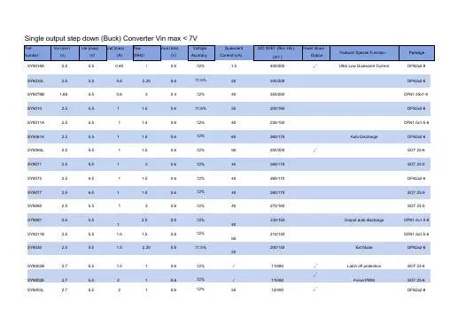
Single output step down (Buck) Converter Vin max < 7V
Part Vin (min) Vin (max) Iout (max) Fsw Vout (min) Voltage Quiescent MO SFET (Ron H/L) Power Good
Number (V) (V) (A) (MHz) (V) Acurracy Current (uA) (m? ) Output Feature/ Special Function Package
SY8018A 2.5 5.5 0.45 / 0.6 ±2% 1.5 400/200 √ Ultra Low Quiescent Current DFN2x2-8
SY8030L 2.5 5.5 0.6 2.25 0.6 ±1.5% 50 300/200
DFN2x2-6
SY8078B 1.85 5.5 0.6 3 0.4 ±2% 40 350/250
DFN1.45x1-6
SY8010 2.5 5.5 1 1.5 0.6 ±1.5% 50 200/150
DFN2x2-6
SY8011A 2.5 5.5 1 1.5 0.6 ±2% 40 230/150
DFN1.5x1.5-6
SY8061A 2.5 5.5 1 1.5 0.6 ±2% 60 260/170
Auto Discharge DFN2x2-6
SY8065L 2.5 5.5 1 1.5 0.6 ±2% 90 250/200 √
SOT 23-6
SY8071 2.5 5.5 1 2 0.6 ±2% 40 260/170
SOT 23-5
SY8075 2.5 6.5 1 1.5 0.6 ±2% 40 260/170
DFN2x2-6
SY8077 2.5 6.5 1 1.5 0.6 ±2% 40 260/170
Absolute Maximum Ratings
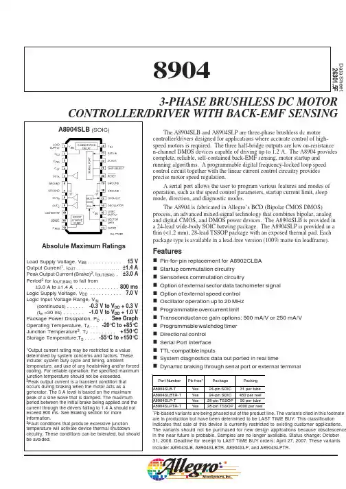
Load Supply Voltage, VBB. . . . . . . . . . . . 15 VOutput Current1, IOUT. . . . . . . . . . . . . . . . . . . . . ±1.4 APeak Output Current (Brake)2, IOUT(BRK). ±3.0 APeriod2 for IOUT(BRK) to fall from ±3.0 A to ±1.4 A. . . . . . . . . . . . . . . 800 msLogic Supply Voltage, VDD. . . . . . . . . . . 7.0 VLogic Input Voltage Range, VIN(continuous). . . . . . -0.3 V to VDD + 0.3 V(tw <30 ns). . . . . . . -1.0 V to VDD + 1.0 VPackage Power Dissipation, PD. . See GraphOperating Temperature, TA. . . -20°C to +85°CJunction Temperature3, TJ. . . . . . . . . +150°CStorage Temperature,TS. . . . -55°C to +150°C
1Output current rating may be restricted to a valuedetermined by system concerns and factors. Theseinclude: system duty cycle and timing, ambienttemperature, and use of any heatsinking and/or forcedcooling. For reliable operation, the specified maximumjunction temperature should not be exceeded.2Peak output current is a transient condition thatoccurs during braking when the motor acts as agenerator. The 3 A level is based on the maximumpeak of a sine wave that is damped. The maximumperiod between the initial brake being applied and thecurrent through the drivers falling to 1.4 A should notexceed 800 ms. See Braking section for moreinformation.3Fault conditions that produce excessive junctiontemperature will activate device thermal shutdowncircuitry. These conditions can be tolerated, but shouldbe avoided.Data Sheet26301.5F