
Wilson-like fermions and the static B_B parameter with no chirality breaking mixings
- 格式:pdf
- 大小:108.32 KB
- 文档页数:3

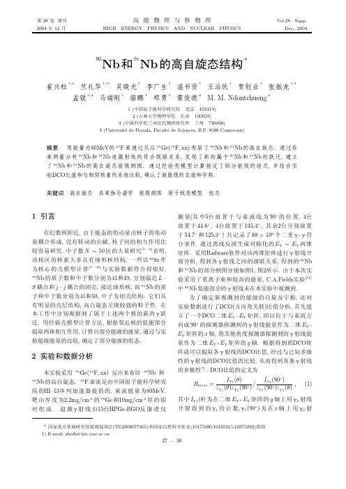
第28卷增刊2004年12月高能物理与核物理HIGH ENERGY PHYSICS AND NUCLEAR PHYSICSVol.28,Supp.Dec.,2004 90Nb和91Nb的高自旋态结构∗崔兴柱1,2竺礼华1;1)吴晓光1李广生1温书贤1王治民1贺创业1张振龙1,2孟锐1,2马瑞刚1骆鹏3郑勇3霍俊德2M.M.Ndontchueng41(中国原子能科学研究院北京102413)2(吉林大学物理学院长春130023)3(中国科学院兰州近代物理研究所兰州730000)4(Universit´e de Douala,Facult´e de Sciences,B.P.8580Cameroun)摘要用能量为80MeV的19F束通过反应76Ge(19F,xn)布居了90Nb和91Nb的高自旋态.通过在束测量分析90Nb和91Nb退激射线的符合级联关系,发现了新的属于90Nb和91Nb的跃迁,建立了90Nb和91Nb的高自旋态能级纲图.通过经验壳模型计算指定了部分能级的组态,并结合实验DCO比值和与相邻核素的系统比较,确认了新能级的自旋和宇称.关键词高自旋态在束伽马谱学能级纲图原子核壳模型组态1引言在幻数核附近,由于能态的角动量由核子的角动量耦合形成,没有转动的贡献,核子间的相互作用比较容易研究.中子数N∼50区的大量研究[1—4]表明,该核区的核素大多具有球形核结构,一些以88Sr作为核心的壳模型计算[5—10]与实验数据符合得很好. 90Nb的质子数和中子数分别为41和49,分别临近L–S耦合和j–j耦合的闭壳,接近球形核,而91Nb的质子和中子数分别为41和50,中子为闭壳结构.它们具有明显的壳层结构,高自旋态呈现较强的粒子性.在本工作中分别观察到了属于上述两个核的新的γ跃迁.用经验壳模型计算方法,根据邻近核的低能部分提取两体相互作用,计算出部分能级的能量,通过与实验能级能量的比较,确定了部分能级的组态.2实验和数据分析本实验采用76Ge(19F,xn)反应来布居90Nb和91Nb的高自旋态.19F束流是由中国原子能科学研究院的HI–13串列加速器提供的,束流能量为80MeV.靶由厚度为2.2mg/cm2的76Ge和10mg/cm2厚的铅衬组成.退激γ射线由15台HPGe-BGO反康谱仪测量(其中5台放置于与束流线为90◦的位置,4台放置于44.6◦,4台放置于135.4◦,其余2台分别放置于54.7◦和125.3◦)共记录了68×106个二重γ-γ符合事件.通过离线反演生成对称化的Eγ∼Eγ两维矩阵.采用Radware软件对该两维矩阵进行γ射线开窗分析,得到各γ射线之间的级联关系,得到的90Nb 和91Nb的部分纲图分别如图1,图2所示.由于本次实验采用了重离子束和较高的能量,C.A.Fields实验[11]中90Nb低能部分的γ射线未在本实验中观测到.为了确定新观测到的能级的自旋及宇称,还对实验数据进行了DCO(方向角关联)比值分析.首先建立了一个DCO二维Eγ-Eγ矩阵,即以位于与束流方向成90◦的探测器探测到的γ射线能量作为二维Eγ-Eγ矩阵的x轴,将其他角度探测器探测到的γ射线能量作为二维Eγ-Eγ矩阵的y轴.根据得到的DCO矩阵就可以提取各γ射线的DCO比值,经过与已知多级性的γ射线的DCO比值的比较,从而得到各条γ射线的多极性[7].DCO比值的定义为R DCO=Iγ1(θ)εγ1(θ)εγ2(90◦)/Iγ1(90◦)εγ1(90◦)εγ2(θ),(1)其中Iγ1(θ)为在二维Eγ-Eγ矩阵的y轴上用γ2射线开窗得到的γ1的计数,γ1(90◦)为在x轴上用γ2射*国家重点基础研究发展规划项目(TG2000077405)和国家自然科学基金(10175090,10105015,10375092)资助1)E-mail:zhulh@27—3028高能物理与核物理(HEP&NP)第28卷线开窗得到的γ1的计数,θ为除90◦外的角度,εγ(θ)为θ角度上所有探测器对γ射线的探测效率.图190Nb的能级纲图图291Nb的能级纲图表1是这次实验中观测到的部分γ射线的DCO比值,通过与已知多级性γ射线的比较即可以定出新得到γ射线的多极性.从表中可以看出,γ射线的DCO比值明显分为两组.DCO比值接近1.5的γ射线对应于∆I=2的跃迁,而DCO比值接近0.5的γ射线则对应于∆I=1的跃迁.表1本次实验部分γ射线的DCO数据E aγI bγR cDCOσλd JπiJπfE ei/keV 90Nb813.4100(10)0.50(0.09)M19+8+813.4 996.326.8(5.2)0.88(0.67)E19−9+1809.7 1067.552.1(7.2) 1.48(0.37)M211−9+1880.9 1249.98.9(3.7)0.78(0.37)M1(10+)9+2062.8 2062.856.3(7.5) 1.61(0.30)E2(10+)8+2062.8 607.18.1(2.8)0.72(0.43)M112−11−2488.0 1876.612.1(3.5) 1.97(1.60)E2(11+)(9+)2690 775.665.2(8.1) 1.35(0.51)E2(12+)(10+)2818.4 495.860.7(7.8)0.57(0.21)M1(13+)(12+)3316.3 626.3 6.3(2.5) 1.30(0.64)E2(13+)(11+)3316.3 676.6 4.5(2.1)0.22(0.16)M1(13+)(12+)3495.0 587.1 5.0(2.5)0.35(0.29)M1(13−)(12−)3075.1 597.58.5(2.9)0.66(0.35)M1(14−)(13−)3672.6 660.437.6(8.2)0.43(0.20)M1(15+)(13+)3976.7 446.412.8(4.2)0.56(0.53)M1(15+)(13+)4423.1 571.414.9(3.8)0.78(0.52)(E2)f(15+)(13+)4066.4 1694.67.0(2.6) 2.23(1.40)E2(17+)(15+)5761.0 384.0 5.3(2.3)0.35(0.25)M1(18+)(17+)6145.0 1904.2 3.3(1.8)0.49(0.31)M1(15−)(14−)5576.8 1774.4 6.6(2.6) 1.66(0.62)E2(17−)(15−)7351.2 743.2 2.1(1.4)0.71(0.44)M1(18−)(17−)8094.4 281.3g 1.1(1.0)8375.7 91Nb(假定2290keV相对强度为100)421.135.8(7.7)0.35(0.17)M1(27/2+)(25/2+)5452.5 1063.414.9(7.3)0.58(0.24)M1f(29/2+)(27/2+)6515.8 919.026.7(5.4)0.62(0.24)M1(31/2+)(29/2+)7434.9 1982.567.1(8.4)0.78(0.32)(E2)f(31/2+)(27/2+)7434.5 661.752.0(7.5)0.43(0.20)M1(33/2+)(31/2+)8095.6 1717.410.0(4.6)0.55(0.29)M1(23/2+)(21/2+)5182.0 904.3 5.7(2.3)0.40(0.15)M1(25/2+)(23/2+)6086.7 2076.215(4.0) 2.53(1.04)E2(21/2−)(21/2+)5541.4 730.110(3.3) 1.29(0.30)E2(25/2−)(21/2−)6271.5 645.39(3)0.48(0.16)M1(27/2−)(25/2−)6919.8 aγ−射线的能量误差约为0.5keV;bγ−射线相对强度;c由多极性为2的γ−射线开窗得到的R DCO值;d由R DCO得出的射线多极性;e衰变能级的能量;f多极性由进一步的系统比较确定; g峰很弱无法确定其多极性.由于DCO数据只能确定γ射线的跃迁多极性,不能指定跃迁是磁跃迁还是电跃迁.通过对邻近的核的能级纲图进行分析,并做系统性比较,推定90Nb 和91Nb中部分能级的自旋和宇称.而在Nillson单粒子能级图中,可以看到N=49的三个核的基态价核子都是位于g9/2轨道的一个质子和一个中子空穴,因此这3个核的能级结构非常相似,如图3所示.而N=50的同中子素具有位于g9/2轨道的一个质子,他们的能级结构也非常相似,如图4.但是,这些核的能级结构存在一些差别,这主要是由于它们的价质子所处的平均场和价核子的激发状态不完全相同.增刊崔兴柱等:90Nb和91Nb的高自旋态结构29图3N=49的临近90Nb的同中子素的纲图比较图4N=50的临近91Nb的同中子素的纲图比较3经验壳模型计算由于90Nb和91Nb的中子数分别为49和50,接近或等于N=50的满壳结构,所以可以用近球形的壳模型的经验公式来描述.选择90Zr作为核芯,通过研究核外价核子的组态,以及由附近核的低激发态提取的价核子间的相互作用以及价核子和声子间的相互作用,来研究90Nb和91Nb的能级结构[12,14].至于不选88Sr作为我们计算的核芯,是因为选90Zr计算比较简单,而计算结果表明其计算结果和实验数据符合很好.对90Nb的10+态能级,其能量可描述为E90Nb{[πg9/2⊗νg−19/2]8+⊗2+}10+=E91Nb[πg9/2⊗2+]11/2++E89Zr[νg−19/2⊗2+]13/2+−E90Zr2++∆(πg9/2⊗νg−19/2)8++S,(2)其中∆(πg9/2⊗νg−19/2)8+=E[πg9/2⊗νg−19/2]8+−(E91Nbπg9/2+E89Zrνg9/2)−S,(3)S=B(90Nb)+B(90Zr)−B(89Zr)−B(91Nb)为质量过剩项.用同样的方法我们可以得到其他的能态的结构.本次计算的部分结果分别列于表2和表3.同时,为了便于比较,我们将计算值也分别在图1,图2中绘出.表290Nb中部分能级壳模型计算值与观测值的比较JπE exp/keV configuration E calc/keV9−1808πg9/2⊗νp−11/2g−19/2s1/2190511−1880πg9/2⊗νp−11/2g−19/2d3/2213212−2487πg9/2⊗νp−11/2g−19/2d5/2252413−3074πp−11/2g29/2⊗νg−19/2305314−3671πf−15/2g29/2⊗νg−19/237709+813πg9/2⊗νg−19/283410+2063[πg9/2⊗νg]8+⊗2+208311+2689[πg9/2⊗νg−19/2]9+⊗2+285712+2818πg9/2⊗νg−29/2s1/2282613+3315πg9/2⊗νg−29/2s1/2333414+未观测πg9/2⊗νg−29/2d3/2363215+4067πg9/2⊗νg−29/2d5/2392317+5761πf−15/2p−11/2g39/2⊗νg−19/2512918+6145πf−15/2p−11/2g39/2⊗νg−19/25900表390Nb中部分能级壳模型计算值与观测值的比较JπE exp/keV configuration E calc/keV27/2+6916πp−11/2g29/2⊗νfg−19/2s1/22627421/2+3465πg9/2⊗νg−19/2d3/2349023/2+5182πg9/2⊗νg−19/2d5/2526725/2+5116πg9/2⊗νg−19/2g7/2503127/2+5452πp−11/2f−15/2g9/2g7/2d5/2553129/2+6515πf−15/2p−13/2g9/2g7/2d5/26382从表2中可以看出四准粒子态的大部分计算与实验得到的能级数据基本相符,但是基于六准粒子态计算的17+和18+两个能态已经偏离了实验数据很多,不过还可以描述大致的规律.这可能是由于组态混杂引起的,也可能是从相邻核中提取剩余相互作用时所选的组态不正确所致.通过上述计算,我们可以进一步确定各能级的自旋及宇称指定的正确性.4结论实验布居了90Nb和91Nb的高自旋态,得到了新的能级结构,实验结果和经验壳模型的计算符合得很好.表明了90Nb和91Nb具有较好的壳层结构,是一个近球形核.通过经验壳模型计算与实验能级的比较确定了一些90Nb和91Nb高自旋态的价核子组态.30高能物理与核物理(HEP&NP)第28卷本工作是在中国原子能科学研究院HI–13串列加速器上完成的,加速器运行组为实验提供稳定的高品质束流,许国基研究员提供了实验靶,在此表示感谢,同时作者还要感谢兰州近代物理研究所的张玉虎、柳敏良等人在经验壳模型计算方面给予的指导和帮助.参考文献(References)1Warburton E K,Olness J W,Lister C J.J.Phys.,1986, G12:10172Tulapurkar A A,Das P,Mishra S N.Phys.Rev.,1996, C54:29043Schubart R,Jungclaus A,Harder A.Nucl.Phys.,1995, A591:5154Ghugre S S,Patel S B,Bhowmik R K.Phys.Rev.,1995, C51:11365JI Xiang-Dong,Wildental B H.Phys.Rev.,1988,C37: 12566B Lomqvist J,Rydstr¨o m L.Phys.Scr.,1985,31:317Muto K,Shimano T,Horie H.Phys.Lett.,1984,135B:3498Stefanova E A,Danchev M,Schwenger R.Phys.Rev., 2002,C65:0343239Johnstone I P,Johnstone L D.Phys.Rev.,1997,C55: 122710Arnell S E,F oltescu D,Roth H A.Phys.Rev.,1994,C49: 5111Fields C A,De Boer F W N,Kraushaar J J.Nucl.Phys., 1981,A363:31112Piiparinen M,Atac A,Blomqvist J.Nucl.Phys.,1986, A605:19113LI Guang-Sheng,Chin.Phys.Lett.,1999,16(11):796 14Bayer S,Byrne A P,Dracoulis G D.Nucl.Phys.,2001, A694:3Study of High Spin States in90Nb and91Nb∗CUI Xing-Zhu1,2ZHU Li-Hua1;1)WU Xiao-Guang1LI Guang-Sheng1WEN Shu-Xian1WANG Zhi-Min1HE Chuang-Ye1ZHANG Zhen-Long1,2MENG Rui1,2MA Rui-Gang1LUO Peng3ZHENG Yong3HUO Jun-De2M.M.Ndontchueng41(China Institute of Atomic Energy,Beijing102413,China)2(Department of Physics,Jilin University,Changchun130023,China)3(Institute of Modern Physics,Chinese Academy of Sciences,Lanzhou730000,China)4(Universit´e de Douala,Facult´e de Sciences,B.P.8580Cameroun)Abstract The high spin states of90Nb and91Nb have been populated via reaction76Ge(19F,xn)atbeam energy of80MeV.The de-excitingγ-rays have been measured with in-beamγ-ray spectroscopymethod.Afterγ-γcoincidence analysis,the new level scheme of90Nb and91Nb was established.Basedon the semi-empirical shell model calculations,the configurations of the levels have been suggested,in addi-tion,the spins and parities of the new levels have been assigned according to the experimental DCO valuesand to the systematic comparison with the neighboring nuclei.Key words high spin state,in-beamγ-ray spectroscopy,level scheme,nuclear shell model,configu-ration*Supported by Major State Basic Research Development Program(TG2000077405)and National Natural Science Foundation of China(10175090,10105015,10375092)1)E-mail:zhulh@。


Band structures and band offsets of high K dielectrics on SiJ.Robertson *Engineering Department,Cambridge University,Trumpington Street,Cambridge CB21PZ,UKAbstractVarious high dielectric constant oxides will be used as insulator in ferroelectric memories,dynamic random access memories,and as the gate dielectric material in future complementary metal oxide semiconductor (CMOS)technology.These oxides which have moderately wide bandgaps provide a good test of our understanding of Schottky barrier heights and band offsets at semiconductor interfaces.Metal induced gap states (MIGS)are found to give a good description of these interfaces.The electronic structure and band offsets of these oxides are calculated.It is found that Ta 2O 5and SrTiO 3have small or vanishing conduction band offsets on 2O 3,Y 2O 3,ZrO 2,HfO 2,Al 2O 3and silicates like ZrSiO 4have offsets over 1.4eV for both electrons and holes,making them better gate dielectrics.#2002Elsevier Science B.V .All rights reserved.Keywords:Band structures;Band offsets;Dielectric constant oxides1.IntroductionThe closed shell transition metal (TM)oxides like SrTiO 3have been extensively studied for their ferro-electric properties,phase transitions and soft modes [1].They are now of great technological importance for electronic devices such as dynamic random access memories (DRAMs),ferroelectric non-volatile mem-ories (FeRAMs),and as alternative gate oxides in future complementary metal oxide semiconductor (CMOS)transistors [2±4].This requires them to be considered in terms of their electronic properties,by treating them as wide bandgap semiconductors [5].This paper reviews the band structures of these oxides,and then considers important electronic prop-erties such as their band offsets and Schottky barrier heights (SBHs).It turns out that the oxides have intermediate bandgaps and so they provide a goodtest of our present models of Schottky barriers and band offsets.2.Band structuresThe simplest band structures are those of the cubic ABO 3perovskites such as SrTiO 3or BaTiO 3.The bandgap is direct at G (Fig.1)[6].The valence band consists mainly of the 2p states of the O 2Àions,and the conduction band of the Ti 4 3d (t 2g )states [7].The Sr s and p states lie higher in the conduction band.However,the bonding is 60±70%ionic,and so there is signi®cant mixing of Ti d states in the valence band.The bands of the Pb perovskites differ in that Pb is divalent and it retains its 6s electrons [8].The ®lled Pb s states form an additional valence band at about À7eV as in PbTiO 3(Fig.2)[6,9].There is also some Pb s admixture in the upper valence band.The empty Pb 6p states now lie near the lowest conduction band.When Zr replaces Ti in SrTiO 3(or BaTiO 3),the bandgap increases strongly by 2eV,because itisApplied Surface Science 190(2002)2±10*Tel.: 44-1223-33-2689;fax: 44-1223-33-2662.E-mail address:jr@ (J.Robertson).0169-4332/02/$±see front matter #2002Elsevier Science B.V .All rights reserved.PII:S 0169-4332(01)00832-7controlled by the energy of the Zr d states.In contrast,in PZT,the Pb 6p states form the conduction band minimum,so the gap barely increases from 3.3to 3.7eV [10].It is recognised that the resonant covalence of Ti-d/O-p states is the origin of ferroelectricity in SrTiO 3type perovskites [11].In Pb perovskites,there is additional resonant covalence between Pb s and O p states which increases the ferroelectric polarity.SrBi 2Ta 2O 9is a layered crystal built from perovs-kite blocks separated by Bi 2O 2layers.It turns out that the Bi s and p states form the highest valence band and lowest conduction bands,respectively,while the ferro-electric response originates mainly from the TaO 3perovskite blocks [12].There is therefore an interest-ing separation of the functionality onto the Ta and Bi sub-lattices.Cubic ZrO 2has the ¯uorite structure.It has a simple band structure,as shown in Fig.3.The O p states form the valence band with a maximum at X [13].The conduction band minimum is at G ,and consists of Zr d states.The Zr d x 2Ày 2and d z 2states lie below the d xy states.The Zr s state lies midway between these at G ,but it disperses rapidly upwards.2.1.Models of Schottky barriers and semiconductor heterojunctionsThe band line-up of two semiconductors is deter-mined,like the SBH of a semiconductor on a metal,by charge transfer across the interface and the presence of any dipole layer at the interface.The charge transfer is that between the metal and the interface states of the semiconductor (Fig.4)[14].The charge transfertendsFig.1.Band structure of BaTiO 3calculated by pseudo-potential method [6].J.Robertson /Applied Surface Science 190(2002)2±103to align the Fermi level E F of the metal to the energy level of the interface states.The SBH for electrons f n between a semiconductor S and a metal M is f n S F M ÀF S F S Àw S(1)Here,F M is the work function of the metal,F S the energy of the semiconductor interface states,w S the semiconductor's electron af®nity (EA)and S the Schottky pinning parameter.S is given by [15]S11 e 2N d =ee 0(2)where e is the electronic charge,e 0the permittivity of free space,N the areal density of the interface states and d their decay length in the semiconductor.The dimensionless pinning factor S describes if the barrieris `pinned'or not.S varies between the limits S 1for unpinned Schottky barriers,and S 0for `Bardeen'barriers pinned by a high density of interface states in which the SBH is f n F S Àw S .There are numerous models of the origins of inter-face states,both intrinsic and extrinsic.In the intrinsic model originating from Bardeen and Heine,a semi-in®nite semiconductor in contact with a metal pos-sesses intrinsic states which are now called metal-induced gap states (MIGS)by Tersoff [14].F S is then the charge neutrality level (CNL)of the interface states,de®ned as the energy above which the states are empty for a neutral surface [16±18].On the other hand,the extrinsic models stress that the metal can react with the semiconductor [19].Brillson correlated the heat of reaction with S .This reaction maycreateFig.2.Band structure of PbTiO 3calculated by pseudo-potential method [6].4J.Robertson /Applied Surface Science 190(2002)2±10interface defects such as vacancies,whose gap states can pin the metal Fermi level,as noted by Spicer [20]and Dow [21].These models were supported by theobservation that pinning occurs even for monolayer coverage of metal,before the MIGS could be estab-lished.It is now believed that,overall,the intrinsic model gives a better description of Schottky barriers,because intrinsic states have a larger pinning dipole,N d ,than surface defects.The pinning parameter S has been in¯uential in our empirical understanding of Schottky barriers.Some years ago,Kurtin et al.[22]noted that S seemed to vary sharply with the ionicity of semi-conductor (Fig.5),from near 0for low ionicity semiconductors like Si and GaAs to 1for higher ionicity solids like SiO 2,SrTiO 3and KTaO 3.S is a dimensionless slope of barrier height to metal work function,S@f n @F M(3)Fig.3.Band structure of ZrO 2calculated by pseudo-potential method[6].Fig.4.Schematic diagram of SBHs.J.Robertson /Applied Surface Science 190(2002)2±105However,Louie [23]and Schluter [24]noted that Kurtin [22]had actually correlated the barrier heights to S H :S H@f n @X(4)which is the slope of barrier height to the Pauling electronegativity of the metal,and not the dimension-less S in (4).The work function and electronegativity vary roughly as [25,26]:F M 2:27X M 0:34(5)Thus,S H 2:27S ,and the Schottky limit should be S H 2:27.The data rarely reach this limit and Schluter [24]observed that S had a better correlation with the dielectric constant of the semiconductor e 0.Empiri-cally,Mo Ènch [14,27]found that S varied with e I as S11 0:1 e I À1 2(6)Certain materials are key tests of Schottky barriermodels.Diamond and xenon [14,28]have zero ioni-city but small e I ,and so their large S values show that S depends on e not on ionicity.This is tested by plotting log 1= S À1 against log e I À1 as in Fig.6.The wide gap oxides provide another key test,because they have intermediate e I values.SrTiO 3and KTaO 3were taken as high ionicity solids in the original Kurtin plot,with S H $1.However,this wasbefore data was actually known.When data [29]became available for SrTiO 3,showing S lying between 0.25and 0.4(Fig.6),it was clear that S is much lower.SrTiO 3falls well on the trend in Fig.3.The reason for this is that the SBHs depend on e I .e I is controlled by the states closest to the bandgap [5].In SrTiO 3,these are the moderately ionic Ti±O states of Ti±O bonds,not the highly ionic Sr±O states which lie well away from the gap and provide a much smaller contribution to e I .This can be seen in the partial density of states (DOS)of SrTiO 3in Fig.6.Thus,SrTiO 3and KTaO 3were misplaced in Fig.5as highly ionic solids.A lesser point is that the moderate value of S of SrTiO 3clearly correlates with e I ,and not with the low frequency dielectric constant e 0,which has a very large value for ferroelectrics and would give S %0from (6).SrTiO 3also serves as an evidence against the defect model,in that the barrier lies some way into the gap,not at the conduction band edge where the O vacancy states lie and would cause pinning.In sum-mary,the MIGS model of Schottky barriers holds for a wide range of solids of various ionicity and dielectric constants [5].The band alignment between two semiconductors is controlled by charge transfer and interface dipoles,just as Schottky barriers [30].For no dipoles,the Schottky limit,the conduction band offset isgivenFig.5.Schottky barrier pinning factor S H in the (incorrect)model of Kurtin etal.Fig. 6.Log±log plot of 1= S À1 vs.e I À1for various semiconductors and insulators to verify the MIGS model of Schottky barrier pinning factor S .6J.Robertson /Applied Surface Science 190(2002)2±10by the difference in their electron af®nities,the `elec-tron af®nity rule'.A similar idea was that for no charge transfer,the band line-ups are derived by placing each semiconductor's band on an absolute energy scale such as those of the free atom energy levels [31].Tersoff [16]showed that the band offset between two semiconductors a and b is controlled by interface dipoles as in the Schottky barrier,and so the conduc-tion band offset is given by f n w a ÀF CNL ;a À w b ÀF CNL ;bS F CNL ;a ÀF CNL ;b(7)The offsets are now described by aligning the CNLs of each semiconductor,modi®ed by the S factor.For simple semiconductors like Si,e I is large,and so S is small and the third term was negligible in the original formulation,but it is retained here for wide gap oxides.For strong pinning,the alignment is just given by the alignment of the two CNLs.The CNL energy below the vacuum level is a measure of the mean electronegativity of the semiconductor,in the same way that the work function of a metal is propor-tional to the metal's electronegativity.Thus,Eq.(7)says that the band alignment is the difference in electronegativity screened by the S factor.A wide ranging quantitative comparison found that the CNL models gives a good description of the band offsets [30].The CNL is the branch point of the semiconductor interface states.It is the integral of the Green's func-tion of the band structure,taken over the Brillouin zone [17],G E ZBZ N E H d H EE ÀE H0(8)Cardona and Christensen later provided a quicker method using a sum over special points of the Bril-louin zone [5,32].G E X i 1E ÀE i (9)2.2.Application to oxidesThe band alignments for the various wide gapoxides in contact with metal or silicon are found by calculating their CNLs and S parameters.The S factors are found from (6)using the experimental values of e Iand are shown in Table 1.The CNLs were found by calculating the oxide band structures by the tight-binding method [5,6,8,33].The tight-binding para-meters are found by ®tting to existing band structures [9,10,34],photoemission spectra and optical data [2,35±37].The CNLs for the various oxides are given in Table 1,together with the experimental values of their bandgaps and electron af®nities [2,38].SrTiO 3is an important oxide for future DRAM capacitor dielectrics.SrTiO 3is also the most studied system and the best test of our calculations.Fig.7compares the predicted SBHs of SrTiO 3on various metals with the experimental values [30,39±43].The experimental data are quite scattered but are quite consistent with S !1and our calculated value of 0.28.This shows that SrTiO 3is a key oxide in the tests of Schottky barrier models.The calculated barrier height for SrTiO 3on Pt is 0.9eV ,which is close to the 0.8eV found by photoemission by Copel et al.[43].However we cannot account for the much larger S value found by Shimizu et al.[42].BaTiO 3has similar band offsets to SrTiO 3.PbTi x Zr 1Àx O 3or PZT is an important ferroelectric for non-volatile memories,optical memories and other applications.The predicted barrier height for Pt onTable 1Calculated values for various oxides of their CNL and conduction band (CB)offset with Si aGap (eV)EA (eV)CNL (eV)e I S CB offset (eV)SiO 290.9 2.250.86 3.5b Si 3N 4 5.3 2.1 4.10.51 2.4b Ta 2O 5 4.4 3.3 3.3 4.840.40.3BaTiO 3 3.3 3.9 2.6 6.10.28À0.1BaZrO 3 5.3 2.6 3.740.530.8TiO 2 3.05 3.9 2.27.80.180.05ZrO 2 5.8 2.5 3.6 4.80.41 1.4HfO 26 2.5 3.740.53 1.5Al 2O 38.81c 5.5 3.40.63 2.8Y 2O 362c 2.4 4.40.46 2.3La 2O 36c 2c 2.440.53 2.3ZrSiO 46.5 2.4 3.6 3.80.56 1.5SrBi 2Ta 2O 94.13.53.35.30.4aExperimental values [36,37]of the bandgap,EA [2,38],dielectric constant e I [37]are also given.In Eqs.(2)and (5),F S is the energy of the CNL below the vacuum level,in this table,it is its energy above the valence band.bExperimental values.cEstimated values.J.Robertson /Applied Surface Science 190(2002)2±107PZT (Pb 0.55Zr 0.45O 3)is 1.45eV ,which is close to the 1.5eV measured by Dey et al.[44].The electron barrier of Pt on PZT is larger than that on BST because its CNL lies lower in the gap.This is because of the different band structure of PZT,in which the Pb 6s and 6p states form the band edges and this tends to lower the CNL.The larger value of the hole barrier than the electron barrier means that PZT thin ®lms can have predominantly electron injection,even though bulk PZT tends to be p-type.SrBi 2Ta 2O 9(SBT)is an important ferroelectric for non-volatile memories [2,45].It does not suffer from the loss of switchable polarisation (fatigue)when used with Pt electrodes,which is a problem for PZT.Note that more recent optical data ®nd that the bandgap of SBT is 4.1eV [2].The Schottky barrier of Pt is predicted to be 1.2eV ,which is essentially the same as that found by photoemission [46].There is an important need for high dielectric constant oxides to act as gate oxides instead of silicon dioxide [3,4].This is because the SiO 2layer is now so thin (2nm),that it no longer acts as a good insulator because of direct tunnelling across it.The solution is to replace SiO 2with a thicker layer of a medium k oxide,with the same equivalent capacitance or `equivalence oxide thickness't ox .The oxides must also satisfy certain other conditions,including chemi-cal stability in contact with Si [47].This rules out Ti and Ta which both react with Si to form SiO 2.The other key requirement is that they act as barriers toboth electrons and holes [5,32].This requires that both their valence and conduction band offsets be over 1eV .There is presently considerable effort to identify the most effective oxide,from a choice of ZrO 2,HfO 2,La 2O 3,Y 2O 3,Al 2O 3and the silicates ZrSiO 4and HfSiO 4.The calculated CB band offsets with Si are given in Table 1and summarised in Fig.8.They are compared in Table 2with recent experimental values [48±53],which is seen to be in good agreement.The important feature of Ta 2O 5and SrTiO 3is that both of them have CB offsets on Si under 1eV ,in fact 0in the case of SrTiO 3.This prediction was recently con®rmed by photoemission data of Chambers et al.[48].This means that SrTiO 3or BST cannot be a good gate oxide.The calculated CB offset for Ta 2O 5is only 0.36eV for Ta 2O 5on Si.This is consistent with recent photoemission data of Miyazaki and Hirose [49].Data for Ta 2O 5gate FETS also showed only a small elec-tron barrier [50].The CB offsets for BST and Ta 2O 5and BST are small or negligible because the bandgap is quite small and the band offsets are so asymmetric.To increasetheparison of calculated and observed SBHs of SrTiO 3on variousmetals.Fig.8.Predicted band offsets of various oxides on Si.Table 2Comparison of calculated and experimental values [48±53]of conduction band offsets on SiCalculatedExperiment References Ta 2O 50.350Miyazaki SrTiO 3À0.1<0.1Chambers ZrO 2 1.4 1.4Miyazaki 2.0Houssa Al 2O 32.82.8Ludeke8J.Robertson /Applied Surface Science 190(2002)2±10CB offset,we must either increase the bandgap or lower the CNL.The gap can be increased by raising the TM d levels,by using4d or5d metals instead of3d metals or using group IIIB metals instead of group IV. We should use zirconates,not titanates.The gap of BaZrO3is2eV wider than BaTiO3.Its offset is0.8eV.A better strategy is to lower the CNL.The CNL is lowered if the metal valence is lowered from4to3. Indeed,in Y2O3and La2O3,the CNL is much lower in the bandgap.Y2O3and La2O3are the oxides with largest CB offsets for reasonable dielectric constants. ZrO2has a bandgap of5.8eV,which is slightly wider than BaZrO3,and it also has a lower metal/ oxygen stoichiometry.This gives a larger CB offset for ZrO2(1.4eV)than BaZrO3,and indeed one which is just high enough.HfO2is similar.The calculated CB offset of1.4eV for ZrO2compares with an experi-mental value of1.4eV from photoemission[51]and a value of2eV by internal photoemission[52].This CB offset is large enough for devices.Zirconium silicate ZrSiO4and hafnium silicate HfSiO4are glassy oxides with bandgaps of $6.5eV.ZrSiO4consists of chains of alternate edge-sharing ZrO4and SiO2tetrahedra,with addi-tional Zr±O bonds between the chains,leading to an overall six-fold Zr coordination.We estimate the bandgap of ZrSiO4to be6.5eV.The calculated CB offsets are1.5eV,slightly more than ZrO2.Al2O3has a bandgap of8eV close to SiO2but with a higher k($9).Its calculated CB offset is2.8eV, which compares exactly with that measured by Ludeke et al.[53].Overall,the agreement between the calculated and subsequent experimental values for CB offsets in Table2is surprisingly good.References[1]M.E.Lines,X.Glass,Ferroelectrics,Oxford UniversityPress,Oxford,1990.[2]J.F.Scott,Ferroelectrics Rev.1(1998)1.[3]G.D.Wilk,R.M.Wallace,J.M.Anthony,J.Appl.Phys.89(2001)5243.[4]A.I.Kingon,J.P.Maria,S.K.Streiffer,Nature406(2000)1032.[5]J.Robertson,J.Vac.Sci.Technol.B18(2000)1785.[6]P.W.Peacock,J.Robertson,Unpublished work.[7]L.F.Mattheis,Phys.Rev.B6(1972)4718.[8]J.Robertson,W.L.Warren,B.A.Tuttle,D.Dimos,D.M.Smyth,Appl.Phys.Lett.63(1993)1519.[9]R.D.King-Smith,D.Vanderbilt,Phys.Rev.B49(1994)5828.[10]J.Robertson,W.L.Warren,B.A.Tuttle,J.Appl.Phys.77(1995)3975.[11]R.E.Cohen,Nature358(1992)136.[12]J.Robertson,C.W.Chen,W.L.Warren,C.D.Gutleben,Appl.Phys.Lett.69(1996)1704.[13]R.H.French,S.J.Glass,F.S.Ohuchi,Y.N.Xu,W.Y.Ching,Phys.Rev.B49(1994)5133.[14]W.MoÈnch,Phys.Rev.Lett.58(1987)1260.[15]W.MoÈnch,Surf.Sci.300(1994)928.[16]A.W.Cowley,S.M.Sze,J.Appl.Phys.36(1965)3212.[17]C.Tejedor,F.Flores,E.Louis,J.Phys.C10(1977)2163.[18]J.Tersoff,Phys.Rev.Lett.52(1984)465.[19]J.Tersoff,Phys.Rev.B30(1984)4874;J.Tersoff,Phys.Rev.B32(1985)6989.[20]L.J.Brillson,Surf.Sci.300(1994)909.[21]W.E.Spicer,T.Kendelewicz,N.Newman,K.K.Chin,I.Lindau,Surf.Sci.168(1986)240.[22]R.E.Allen,O.F.Sankey,J.D.Dow,Surf.Sci.168(1986)376.[23]S.Kurtin,T.C.McGill,C.A.Mead,Phys.Rev.Lett.30(1969)1433.[24]S.G.Louie,J.R.Chelikowsky,M.L.Cohen,Phys.Rev.B15(1977)2154.[25]M.Schluter,Phys.Rev.B17(1978)5044;M.Schluter,Thin Solid Films93(1982)3.[26]W.Gordy,W.J.O.Thomas,Phys.Rev.24(1956)439.[27]H.B.Michaelson,J.Appl.Phys.48(1977)4729.[28]W.MoÈnch,Phys.Rev.Lett.58(1986)1260.[29]W.MoÈnch,Europhys.Lett.27(1994)479.[30]R.C.Neville,C.A.Mead,J.Appl.Phys.43(1972)4657.[31]W.A.Harrison,J.Vac.Sci.Technol.14(1977)1016.[32]M.Cardona,N.E.Christensen,Phys.Rev.B35(1987)6182.[33]E.T.Yu,J.O.McCaldin,T.C.McGill,Solid State Phys.46(1992)1.[34]J.Robertson,C.W.Chen,Appl.Phys.Lett.74(1999)1168.[35]G.M.Rignanese,X.Gonze,A.Pasquarello,Phys.Rev.B63(2001)104305.[36]R.H.French,J.Am.Ceram.Soc.73(1990)477.[37]E.D.Palik,Handbook of Optical Properties of Solids,V ol.1±3,Academic Press,New York,1985.[38]W.Schmickler,J.W.Schultze,in:J.M.O'Bockris(Ed.),Modern Aspects of Electrochemistry,V ol.17,Plenum Press, London,1986.[39]G.W.Dietz,W.Antpohler,M.Klee,R.Waser,J.Appl.Phys.78(1995)6113.[40]H.Hasegawa,T.Nishino,J.Appl.Phys.69(1991)1501.[41]K.Abe,S.Komatsu,Jpn.J.Appl.Phys.31(1992)2985.[42]T.Shimizu,N.Gotoh,N.Shinozaki,H.Okushi,App.Surf.Sci.117(1997)400;()T.Shimizu,N.Gotoh,N.Shinozaki,H.Okushi,Mat.Res.Soc.Symp.Proc.(2000).[43]M.Copel,P.R.Duncombe,D.A.Neumayer,T.M.Shaw,R.M.Tromp,Appl.Phys.Lett.70(1997)3227.[44]S.K.Dey,J.J.Lee,P.Alluri,Jpn.J.Appl.Phys.34(1995)3134.[45]C.A.Paz de Araujo,J.D.Cuchiaro,L.D.McMillan,M.C.Scott,J.F.Scott,Nature374(1995)627.[46]C.D.Gutleben,Appl.Phys.Lett.71(1997)3444.[47]H.J.Hubbard,D.G.Schlom,J.Mater.Res.11(1996)2757.J.Robertson/Applied Surface Science190(2002)2±109[48]S.A.Chambers,Y.Liang,Z.Yu,R.Dropad,J.Ramdani,K.Eisenbeiser,Appl.Phys.Lett.77(2000)1662.[49]S.Miyazaki,Appl.Surface Science(2002)``these proceed-ings''.[50]S.Miyazaki,M.Narasaki,M.Ogasawara,M.Hirose,Microelec.Eng.59(2001)373.[51]A.Chatterjee,et al.,IEDM Tech Digest,1998,p.777.[52]M.Houssa,M.Tuominen,M.Nailli,V.Afansev, A.Stesmans,J.Appl.Phys.87(2000)8615.[53]R.Ludeke,M.T.Cuberes,E.Cartier,Appl.Phys.Lett.76(2000)2886;D.J.Maria,J.Appl.Phys.45(1974)5454.10J.Robertson/Applied Surface Science190(2002)2±10。
PART ONE 填空问题Q01_01_001 原胞中有p 个原子。
那么在晶体中有3支声学波和33p −支光学波?Q01_01_002 按结构划分,晶体可分为7大晶系, 共14布喇菲格子?Q01_01_004 面心立方原胞的体积为314a Ω=;其第一布里渊区的体积为334(2)*a πΩ= Q01_01_005 体心立方原胞的体积为32a Ω=;第一布里渊区的体积为332(2)*a πΩ= Q01_01_006 对于立方晶系,有简单立方、体心立方和面心立方三种布喇菲格子。
Q01_01_007 金刚石晶体是复式格子,由两个面心立方结构的子晶格沿空间对角线位移 1/4 的长度套构而成,晶胞中有8个碳原子。
Q01_01_008 原胞是最小的晶格重复单元。
对于布喇菲格子,原胞只包含1个原子;Q01_01_009 晶面有规则、对称配置的固体,具有长程有序特点的固体称为晶体;在凝结过程中不经过结晶(即有序化)的阶段,原子的排列为长程无序的固体称为非晶体。
由晶粒组成的固体,称为多晶。
Q01_01_010 由完全相同的一种原子构成的格子,格子中只有一个原子,称为布喇菲格子。
满足ij j i b a πδ2=⋅G G ⎩⎨⎧≠===)(0)(2j i j i π 关系的1b G ,2b G ,3b G 为基矢,由322211b h b h b h G h K K K K ++=构成的格子,称作倒格子。
由若干个布喇菲格子相套而成的格子,叫做复式格子。
其原胞中有两个以上的原子。
Q01_03_001 由N 个原胞构成的晶体,原胞中有l 个原子,晶体共有3lN 个独立振动的正则频率。
Q01_03_002 声子的角频率为ω,声子的能量和动量表示为ω=和q K =。
Q01_03_003 光学波声子又可以分为纵光学波声子和横光学波声子,它们分别被称为极化声子和电磁声子Q01_03_004 一维复式原子链振动中,在布里渊区中心和边界,声学波的频率为 ⎪⎩⎪⎨⎧→±==0,02,)2(211q a q M πβω;光学波的频率⎪⎪⎩⎪⎪⎨⎧±=→=a q m q 2)2(0)2(21212πβµβωQ01_04_001 金属的线度为L ,一维运动的自由电子波函数ikx e Lx 1)(=ψ;能量m k E 222==;波矢的取值Ln k π2= Q01_04_002 电子在三维周期性晶格中波函数方程的解具有()()ik r kr e u r k ψ⋅=K K K K K K 形式?式中()k u r K K 在晶格平移下保持不变。