
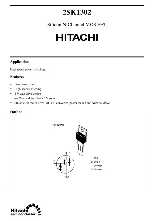
2SK1302中文资料
- 格式:pdf
- 大小:53.14 KB
- 文档页数:9

==99-10-28== P&S
Î人Á¦Ô´µç×ӹɷÝÓÐÏÞ¹«Ë¾ ==13-1==
P&S Î人Á¦Ô´µç×ӹɷÝÓÐÏÞ¹«Ë¾ µØÖ·:ºþ±±Î人ÊÐ׿µ¶ÈªÂ·15ºÅ ÐÅÏä:Î人ÊÐ70020ÐÅÏä Óʱà:
430079 µç»°:(86) (027£©87493500¡«87493506 ´«Õæ:(86) (027) 87491166, 87493497 P&SÍøÍøÖ·:DS1302
¸ßÐÔÄÜ¡¢µÍ¹¦ºÄ´øRAMʵʱʱÖÓоƬ
Ò»¡¢¸ÅÊö
1.1 ÌØÐÔ
l ʵʱʱÖÓ£¬¿É¶ÔÃë¡¢·Ö¡¢Ê±¡¢ÈÕ¡¢ÖÜ¡¢ÔÂÒÔ¼°´øÈòÄê²¹³¥µÄÄê½øÐмÆÊý
l ÓÃÓÚ¸ßËÙÊý¾ÝÔÝ´æµÄ31¡Á8 RAM
l ×îÉÙÒý½ÅÊýµÄ´®ÐÐI/O
l 2.5-5.5VÂú¶È¹¤×÷·¶Î§
¡ª¡ª»¹ÓÐ2.0-5.5VÂú¶È¹¤×÷·¶Î§¿É¹©Ñ¡ÓÃ
l 2.5VʱºÄµçСÓÚ300nA
l ÓÃÓÚʱÖÓ»òRAMÊý¾Ý¶Á/дµÄµ¥×Ö½Ú»ò¶à×Ö½Ú£¨Âö³å·½Ê½£©Êý¾Ý´«ËÍ
l 8Òý½ÅDIP»ò¿ÉÑ¡µÄÓÃÓÚ±íÃæ°²×°µÄ8Òý½ÅSOIC·â×°
l ¼òµ¥µÄ3Ïß½Ó¿Ú
l TTL¼æÈÝ£¨VCC=5V£©
l ¿ÉÑ¡µÄ¹¤ÒµÎ¶ȷ¶Î§-40¡æÖÁ+85¡æ
l ÓëDS1202¼æÈÝ
l ÔÚDS1202»ù´¡ÉÏÔö¼ÓµÄÌصã
¡ª¡ª¿ÉÑ¡µÄÂýËÙ³äµç£¨ÖÁVCC1£©µÄÄÜÁ¦
¡ª¡ªÓÃÓÚÖ÷µçÔ´ºÍ±¸·ÝµçÔ´µÄË«µçÔ´Òý½Å
¡ª¡ª±¸·ÝµçÔ´Òý½Å¿ÉÓÃ×÷µç³Ø»ò³¬ÈÝÁ¿µçÈÝÆ÷£¨Super Cap£©µÄÊäÈë¶Ë
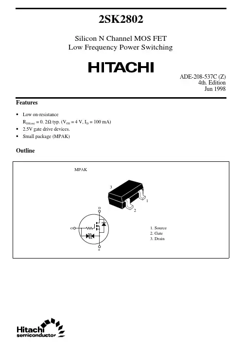
2SK2802
Silicon N Channel MOS FETLow Frequency Power Switching
ADE-208-537C (Z)4th. EditionJun 1998
Features
• Low on-resistance
RDS(on) = 0. 2Ω typ. (VGS = 4 V, ID = 100 mA)
• 2.5V gate drive devices.
• Small package (MPAK)
Outline
1
23
1. Source2. Gate3. DrainMPAK
D
SG2SK2802
2Absolute Maximum Ratings (Ta = 25°C)
ItemSymbolRatingsUnit
Drain to source voltageVDSS30V
Gate to source voltageVGSS±10V
Drain currentID0.5A
Drain peak currentID(pulse)Note11.0A
Channel dissipationPch Note2150mW
Channel temperatureTch150°C
Storage temperatureTstg–55 to +150°C
Note:1.PW ≤ 10µs, duty cycle ≤ 1 %
Electrical Characteristics (Ta = 25°C)
ItemSymbolMinTypMaxUnitTest Conditions
Drain to source breakdownvoltageV(BR)DSS30——VID = 100µA, VGS = 0
Gate to source breakdownvoltageV(BR)GSS±10——VIG = ±100µA, VDS = 0
Zero gate voltege draincurrentIDSS——1.0µAVDS = 30 V, VGS = 0
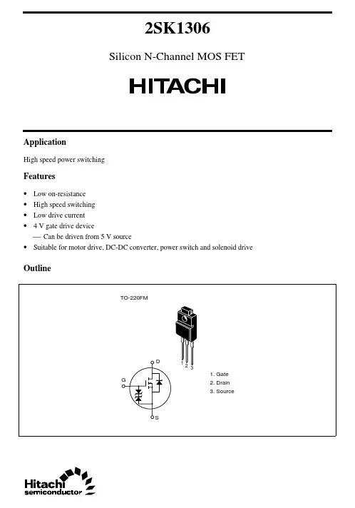
2SK1306Silicon N-Channel MOS FET
Application
High speed power switching
Features
• Low on-resistance
• High speed switching
• Low drive current
• 4 V gate drive device
Can be driven from 5 V source
• Suitable for motor drive, DC-DC converter, power switch and solenoid drive
Outline
123TO-220FM
1. Gate2. Drain3. SourceD
G
S2SK1306
2Absolute Maximum Ratings (Ta = 25°C)
ItemSymbolRatingsUnit
Drain to source voltageVDSS100V
Gate to source voltageVGSS±20V
Drain currentID15A
Drain peak currentID(pulse)*160A
Body to drain diode reverse drain currentIDR15A
Channel dissipationPch*230W
Channel temperatureTch150°C
Storage temperatureTstg–55 to +150°C
Notes:1.PW ≤ 10 µs, duty cycle ≤ 1%2.Value at TC = 25°C2SK1306
3Electrical Characteristics (Ta = 25°C)
ItemSymbolMinTypMaxUnitTest conditions
Drain to source breakdownvoltageV(BR)DSS100——VID = 10 mA, VGS = 0
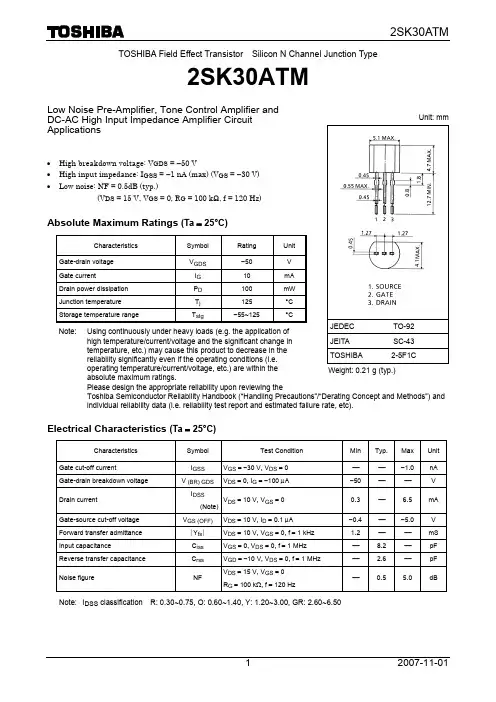
2SK30ATM
2007-11-01 1 TOSHIBA Field Effect Transistor Silicon N Channel Junction Type
2SK30ATM
Low Noise Pre-Amplifier, Tone Control Amplifier and DC-AC High Input Impedance Amplifier Circuit Applications
• High breakdown voltage: VGDS = −50 V • High input impedance: IGSS = −1 nA (max) (VGS = −30 V) • Low noise: NF = 0.5dB (typ.) (VDS = 15 V, VGS = 0, RG = 100 kΩ, f = 120 Hz) Absolute Maximum Ratings (Ta = 25°C) Characteristics Symbol Rating
Unit
Gate-drain voltage VGDS −50 V
Gate current IG 10 mA
Drain power dissipation PD 100 mW
Junction temperature Tj 125 °C
Storage temperature range Tstg −55~125 °C
Note: Using continuously under heavy loads (e.g. the application of high temperature/current/voltage and the significant change in temperature, etc.) may cause this product to decrease in the reliability significantly even if the operating conditions (i.e. operating temperature/current/voltage, etc.) are within the absolute maximum ratings. Please design the appropriate reliability upon reviewing the Toshiba Semiconductor Reliability Handbook (“Handling Precautions”/“Derating Concept and Methods”) and individual reliability data (i.e. reliability test report and estimated failure rate, etc). Electrical Characteristics (Ta = 25°C)