
DS-qian-1.5-1.7
- 格式:pdf
- 大小:130.15 KB
- 文档页数:58


HWD2171 ——设有关断功能的1.5W音频功率放大器●产品概述--- HWD2171是一款单通道桥式连接音频功率放大器,在5V单电源条件下,可为3Ω负载提供1.5W的连续平均功率,THD+N<10% 。
--- HWD2171不需要耦合电容和自举电容,因此非常适用于以小功耗作为主要指标的低电压便携式系统。
--- HWD2171设有低功耗关断模式,可处于I Q=0.6µA的微功耗状态,它通过在SHUTDOWN管脚输入逻辑高电平实现。
另外,HWD2171还具有内部过热停机保护、开关机切换噪声抑制等功能特点。
其增益可以通过外部电阻进行配置。
●技术规格·输出功率 PO (5.0V & 10% THD+N)8Ω 1.5W(典型)uA(典型)·关断电流 0.1·电源范围 2.0V~5.5V·总谐波失真+噪声(1KHz 1W 8Ω) 0.5%●功能特色·极低的待机电流·不需要输出耦合电容,缓冲器网络和自举电容·过热停机保护·单位增益稳定·增益可外部配置·SOP封装·管脚与HWD2161兼容●应用范围·掌上电脑、笔记本·台式机·低压音响系统●工作范围·温度范围﹣40℃~85℃·电源电压 2.0V≤V DD≤5.5V●典型应用●管脚定义●极限参数·电源电压 6.0V·贮存温度-65℃~+150℃·输入电压-0.3V ~V DD+0.3V·功耗内部限制·ESD承受能力(人体模式) 2000V·ESD承受能力(机械模式) 200V·结温150℃●电学特性·电学参数(V DD=5V)除特殊说明外,极限参数在T A=25℃时得出,以下相同。
符号 参数 条件 最小典型 最大 单位I DD静态电源电流 V IN=0V, I O=0A6.510mAI SD关断电流 V SHUTDOWN=V DD0.62.0uA V OS输出失调电压 V IN=0V,无负载 -505.050mVTHD=1%, f=1kHzHWD2171, RL=8Ω 1.2 WP O输出功率THD=10%, f=1kHzHWD2171, RL=8Ω 1.5WTHD+N 总谐波失真+噪音20Hz≤f≤20KHz, A VD=2HWD2171, R L=8Ω, Po=1W0.25 %PSRR 电源抑制比 VDD = 4.9V~5.1V 60 dB●特别说明外部组件描述器件 功能描述1 R IN反相输入电阻,与R f设定闭环增益,并与C IN组成高通滤波器2 C IN阻直流输入耦合电容,与R IN组成高通滤波器fc = 1/(2πR IN C IN).3 R f反馈电阻,与R IN设定闭环增益4 C S电源旁路电容,提供电源滤波5 C BYPASS旁路电容,提供半电压滤波封装规格<SOP-8>:<SOP-8> Top View<SOP-8> Side View 1 <SOP-8> Side View 2Dimensions In Millimeters Dimensions In Inches SymbolMin. Max. Min. Max.A 1.350 1.750 0.053 0.069A1 0.100 0.250 0.004 0.010 A2 1.350 1.550 0.053 0.061b 0.330 0.510 0.013 0.020c 0.170 0.250 0.006 0.010D 4.700 5.100 0.185 0.200e 1.270(BSC) 0.050(BSC)E 3.800 4.000 0.150 0.157E1 5.800 6.200 0.228 0.244 L 0.400 1.270 0.016 0.050 0° 8° 0° 8°Order Number HWD2171M----------------------------------------------------------------------------------------------------------------------。
General DescriptionThe DS17285, DS17485, DS17885, DS17287, DS17487,and DS17887 real-time clocks (RTCs) are designed to be successors to the industry-standard DS12885 and DS12887. The DS17285, DS17485, and DS17885 (here-after referred to as the DS17x85) provide a real-time clock/calendar, one time-of-day alarm, three maskable interrupts with a common interrupt output, a programma-ble square wave, and 114 bytes of battery-backed NV SRAM. The DS17x85 also incorporates a number of enhanced functions including a silicon serial number,power-on/off control circuitry, and 2k, 4k, or 8kbytes of battery-backed NV SRAM. The DS17287, DS17487, and DS17887 (hereafter referred to as the DS17x87) integrate a quartz crystal and lithium energy source into a 24-pin encapsulated DIP package. The DS17x85 and DS17x87power-control circuitry allows the system to be powered on by an external stimulus such as a keyboard or by a time-and-date (wake-up) alarm. The PWR output pin is triggered by one or either of these events, and is used to turn on an external power supply. The PWR pin is under software control, so that when a task is complete, the sys-tem power can then be shut down.For all devices, the date at the end of the month is auto-matically adjusted for months with fewer than 31 days,including correction for leap years. It also operates in either 24-hour or 12-hour format with an AM/PM indicator.A precision temperature-compensated circuit monitors the status of V CC . If a primary power failure is detected,the device automatically switches to a backup supply. A lithium coin cell battery can be connected to the V BAT input pin on the DS17x85 to maintain time and date oper-ation when primary power is absent. The DS17x85 and DS17x87 include a V BAUX input used to power auxiliary functions such as PWR control. The device is accessed through a multiplexed byte-wide interface.ApplicationsEmbedded Systems Utility Meters Security SystemsNetwork Hubs, Bridges, and RoutersFeatures♦Incorporates Industry-Standard DS12887 PC Clock Plus Enhanced Functions ♦RTC Counts Seconds, Minutes, Hours, Day, Date,Month, and Year with Leap Year Compensation Through 2099♦Optional +3.0V or +5.0V Operation ♦SMI Recovery Stack ♦64-Bit Silicon Serial Number♦Power-Control Circuitry Supports System Power-On from Date/Time Alarm or Key Closure ♦Crystal Select Bit Allows Operation with 6pF or 12.5pF Crystal ♦12-Hour or 24-Hour Clock with AM and PM in 12-Hour Mode ♦114 Bytes of General-Purpose, Battery-Backed NV SRAM ♦Extended Battery-Backed NV SRAM2048 Bytes (DS17285/DS17287)4096 Bytes (DS17485/DS17487)8192 Bytes (DS17885/DS17887)♦RAM Clear Function♦Interrupt Output with Six Independently Maskable Interrupt Flags ♦Time-of-Day Alarm Once per Second to Once per Day ♦End of Clock Update Cycle Flag ♦Programmable Square-Wave Output♦Automatic Power-Fail Detect and Switch Circuitry ♦Available in PDIP, SO, or TSOP Package (DS17285, DS17485, DS17885)♦Optional Encapsulated DIP (EDIP) Package with Integrated Crystal and Battery (DS17287,DS17487, DS17887)♦Optional Industrial Temperature Range Available ♦Underwriters Laboratory (UL) RecognizedDS17285/DS17287/DS17485/DS17487/DS17885/DS17887Real-Time Clocks______________________________________________Maxim Integrated Products 1Rev 0; 4/06For pricing, delivery, and ordering information,please contact Maxim/Dallas Direct!at 1-888-629-4642, or visit Maxim’s website at .Ordering Information, Pin Configurations, and Typical Operating Circuit appear at end of data sheet.D S 17285/D S 17287/D S 17485/D S 17487/D S 17885/D S 17887Real-Time Clocks 2_____________________________________________________________________ABSOLUTE MAXIMUM RATINGSDC ELECTRICAL CHARACTERISTICS(V= +4.5V to +5.5V, or V = +2.7V to +3.7V, T = Over the operating temperature range, unless otherwise noted.Typical Stresses beyond those listed under “Absolute Maximum Ratings” may cause permanent damage to the device. These are stress ratings only, and functional operation of the device at these or any other conditions beyond those indicated in the operational sections of the specifications is not implied. Exposure to absolute maximum rating conditions for extended periods may affect device reliability.Voltage Range on V CC Pin Relative to Ground....-0.3V to +6.0V Operating Temperature Range (Noncondensing)Commercial.........................................................0°C to +70°C Industrial..........................................................-40°C to +85°CStorage Temperature.........................................-55°C to +125°C Soldering Temperature.....................See IPC/JEDEC J-STD-020Specification (Note 1)Soldering Temperature (leads, 10 seconds)...................+260°CDC ELECTRICAL CHARACTERISTICSDS17285/DS17287/DS17485/DS17487/DS17885/DS17887Real-Time ClocksAC ELECTRICAL CHARACTERISTICSD S 17285/D S 17287/D S 17485/D S 17487/D S 17885/D S 17887Real-Time Clocks 4_____________________________________________________________________AC ELECTRICAL CHARACTERISTICSWrite TimingDS17285/DS17287/DS17485/DS17487/DS17885/DS17887Real-Time Clocks_____________________________________________________________________5Read TimingPower-Up/Power-Down TimingD S 17285/D S 17287/D S 17485/D S 17487/D S 17885/D S 17887Real-Time Clocks 6_____________________________________________________________________POWER-UP/POWER-DOWN CHARACTERISTICS(T A = -40°C to +85°C) (Note 2)CAPACITANCENote 1:RTC modules can be successfully processed through conventional wave-soldering techniques as long as temperature exposure to the lithium energy source contained within does not exceed +85°C. However, post-solder cleaning with water-washing techniques is acceptable, provided that ultrasonic vibrations not used to prevent damage to the crystal.Note 2:Limits at -40°C are guaranteed by design and not production tested.Note 3:All voltages are referenced to ground.Note 4:All outputs are open.Note 5:Specified with CS = RD = WR = V CC , ALE, AD0–AD7 = 0.Note 6:Applies to the AD0–AD7 pins, IRQ , and SQW when each is in a high-impedance state.Note 7:Measured with a 32.768kHz crystal attached to X1 and X2.Note 8:Measured with a 50pF capacitance load plus 1TTL gate.Note 9:If the oscillator is disabled in software, or if the countdown chain is in reset, t REC is bypassed, and the part becomesimmediately accessible.Note 10:Guaranteed by design. Not production tested.data.DS17285/DS17287/DS17485/DS17487/DS17885/DS17887Real-Time Clocks_____________________________________________________________________7SUPPLY CURRENT vs. INPUT VOLTAGEV BAT (V)S U P P L Y C U R R E N T (n A )3.53.33.02.82503003504002002.53.8SUPPLY CURRENT vs. TEMPERATURETEMPERATURE (°C)S U P P L Y C U R R E N T (n A )655035205-10-25300350400250-4080OSCILLATOR FREQUENCY vs. SUPPLY VOLTAGED S 17285/87 t o c 03SUPPLY VOLTAGE (V)O S C I L L A T O R F R E Q U E N C Y (H z )5.04.54.03.53.032768.132768.232768.332768.432768.532768.632768.732768.02.55.5Typical Operating Characteristics(V CC = +3.3V, T A = +25°C, unless otherwise noted.)D S 17285/D S 17287/D S 17485/D S 17487/D S 17885/D S 17887Real-Time Clocks 8_____________________________________________________________________Pin Description (continued)DS17285/DS17287/DS17485/DS17487/DS17885/DS17887Real-Time ClocksD S 17285/D S 17287/D S 17485/D S 17487/D S 17885/D S 17887Real-Time Clocks 10____________________________________________________________________Figure 1. Functional DiagramDetailed DescriptionThe DS17x85 is a successor to the DS1285 real-time clock (RTC). The device provides 18 bytes of real-time clock/calendar, alarm, and control/status registers and 114 bytes of nonvolatile battery-backed RAM. The device also provides additional extended RAM in either 2k/4k/8kbytes (DS17285/DS17485/DS17885). A time-of-day alarm, six maskable interrupts with a common interrupt output, and a programmable square-wave output are available. It also operates in either 24-hour or 12-hour format with an AM/PM indicator. A precision temperature-compensated circuit monitors the status of V CC . If a primary power-supply failure is detected, the device automatically switches to a backup supply. The backup supply input supports a primary battery, such as a lithium coin cell. The device is accessed by a mul-tiplexed address/data bus.Oscillator CircuitThe DS17x85 uses an external 32.768kHz crystal. The oscillator circuit does not require any external resistors or capacitors to operate. Table 1 specifies several crystal parameters for the external crystal, and Figure 2shows a functional schematic of the oscillator circuit.The oscillator is controlled by an enable bit in the con-trol register. Oscillator startup times are highly depen-dent upon crystal characteristics, PC board leakage,and layout. High ESR and excessive capacitive loads are the major contributors to long startup times. A cir-cuit using a crystal with the recommended characteris-tics and proper layout usually starts within one second.An external 32.768kHz oscillator can also drive the DS17x85. In this configuration, the X1 pin is connected to the external oscillator signal and the X2 pin is floated.Clock AccuracyThe accuracy of the clock is dependent upon the accu-racy of the crystal and the accuracy of the match between the capacitive load of the oscillator circuit and the capacitive load for which the crystal was trimmed.Additional error will be added by crystal frequency drift caused by temperature shifts. External circuit noise coupled into the oscillator circuit may result in the clock running fast. Figure 3 shows a typical PC board layout for isolation of the crystal and oscillator from noise.Refer to Application Note 58: Crystal Considerations with Dallas Real-Time Clocks for detailed information.Clock Accuracy (DS17287, DS17487, and DS17887)The encapsulated DIP (EDIP) modules are trimmed at the factory to ±1 minute per month accuracy at 25°C.DS17285/DS17287/DS17485/DS17487/DS17885/DS17887Real-Time ClocksFigure 2. Oscillator Circuit Showing Internal Bias NetworkFigure 3. Layout ExampleD S 17285/D S 17287/D S 17485/D S 17487/D S 17885/D S 17887Power-Down/Power-UpConsiderationsThe RTC function continues to operate, and all the RAM, time, calendar, and alarm memory locations remain nonvolatile regardless of the level of the V CC input. V BAT or V BAUX must remain within the minimum and maximum limits when V CC is not applied. When V CC falls below V PF , the device inhibits all access,putting the part into a low-power mode. When V CC is applied and exceeds V PF (power-fail trip point), the device becomes accessible after t REC , if the oscillator is running and the oscillator countdown chain is not in reset (Register A). This time period allows the system to stabilize after power is applied. If the oscillator is not enabled, the oscillator enable bit is enabled on power-up, and the device becomes immediately accessible.Power ControlThe power control function is provided by a precise,temperature-compensated voltage reference and a comparator circuit that monitors the V CC level. The device is fully accessible and data can be written and read when V CC is greater than V PF . However, when V CC falls below V PF , the device inhibits read and write access. If V PF is less than V BAT , the device power is switched from V CC to the higher of V BAT or V BAUX when V CC drops below V PF . If V PF is greater than the higher of V BAT or V BAUX , the device power is switched from V CC to the higher of V BAT or V BAUX when V CC drops below the higher backup source. The registers are maintained from the V BAT or V BAUX source until V CC is returned to nominal levels. After V CC returns above V PF , read and write access is allowed after t REC .Time, Calendar, and AlarmLocationsThe time and calendar information is obtained by read-ing the appropriate register bytes. The time, calendar,and alarm are set or initialized by writing the appropri-ate register bytes. The contents of the 12 time, calen-dar, and alarm bytes can be either binary or binary-coded decimal (BCD) format. Tables 3A and 3B show the BCD and binary formats of the 12 time, date,and alarm registers, control registers A to D, plus the two extended registers that reside in bank 1 only (bank 0 and bank 1 switching is explained later in this text).The day-of-week register increments at midnight, incre-menting from 1 through 7. The day-of-week register is used by the daylight saving function, and so the value 1 is defined as Sunday. The date at the end of the month is automatically adjusted for months with fewer than 31 days, including correction for leap years.Before writing the internal time, calendar, and alarm registers, the SET bit in Register B should be written to logic 1 to prevent updates from occurring while access is being attempted. In addition to writing the 12 time,calendar, and alarm registers in a selected format (binary or BCD), the data mode bit (DM) of Register B must be set to the appropriate logic level. All 12 time,calendar, and alarm bytes must use the same data mode. The set bit in Register B should be cleared after the data mode bit has been written to allow the real time clock to update the time and calendar bytes. Once initialized, the real time clock makes all updates in the selected mode. The data mode cannot be changed without reinitializing the 12 data bytes. Tables 3A and 3B show the BCD and binary formats of the 12 time,calendar, and alarm locations.The 24-12 bit cannot be changed without reinitializing the hour locations. When the 12-hour format is selected,the high order bit of the hours byte represents PM when it is logic 1. The time, calendar, and alarm bytes are always accessible because they are double-buffered.Once per second, the eight bytes are advanced by one second and checked for an alarm condition.If a read of the time and calendar data occurs during an update, a problem exists where seconds, minutes,hours, etc., may not correlate. The probability of read-ing incorrect time and calendar data is low. Several methods of avoiding any possible incorrect time and calendar reads are covered later in this text.Real-Time ClocksThe alarm bytes can be used in two ways. First, when the alarm time is written in the appropriate hours, min-utes, and seconds alarm locations, the alarm interrupt is initiated at the specified time each day, if the alarm enable bit is high. In this mode, the “0” bits in the alarm registers and the corresponding time registers must always be written to 0 (see Table3A and 3B). Writing the 0 bits in the alarm and/or time registers to 1 can result in undefined operation.The second use condition is to insert a “don’t care”state in one or more of the alarm bytes. The don’t care code is any hexadecimal value from C0 to FF. The two most significant bits of each byte set the don’t care condition when at logic 1. An alarm will be generated each hour when the “don’t care” bits are set in the hours byte. Similarly, an alarm is generated every minute with don’t care codes in the hours and minute alarm bytes. An alarm is generated every second with don’t care codes in the hours, minutes, and seconds alarm bytes.All 128 bytes can be directly written or read except for the following:1)Registers C and D are read-only.2)Bit 7 of register A is read-only.3)The MSB of the seconds byte is read-only.DS17285/DS17287/DS17485/DS17487/DS17885/DS17887Real-Time Clockster, 0 bits in the time and date registers can be written to 1, but can be modified when the clock updates. 0 bits should always be written to 0 except for alarm mask bits.flag that can be monitored. When the UIP bit is 1, the update transfer will soon occur. When UIP is 0, the update transfer does not occur for at least 244µs. The time, calendar, and alarm information in RAM is fully available for access when the UIP bit is 0. The UIP bit is read-only. Writing the SET bit in Register B to 1 inhibits any update transfer and clears the UIP status bit.used to turn the oscillator on or off and to reset the countdown chain. A pattern of 01X is the only combina-tion of bits that turns the oscillator on and allows the RTC to keep time. A pattern of 11X enables the oscillator but holds the countdown chain in reset. The next update occurs at 500ms after a pattern of 01X is written to DV0,DV1, and DV2. DV0 is used to select bank 0 or bank 1 as defined in Table 5. When DV0 is set to 0, bank 0 is selected. When DV0 is set to 1, bank 1 is selected.D S 17285/D S 17287/D S 17485/D S 17487/D S 17885/D S 17887Real-Time Clocks written to 0 except for alarm mask bits.Control RegistersThe four control registers (A, B, C, and D) reside inboth bank 0 and bank 1. These registers are accessi-ble at all times, even during the update cycle.Register A (0Ah)Bits 3 to 0: Rate Selector Bits (RS3 to RS0). These four rate-selection bits select one of the 13 taps on the 15-stage divider or disable the divider output. The tap selected can be used to generate an output square wave (SQW pin) and/or a periodic interrupt. The user can do one of the following:1)Enable the interrupt with the PIE bit;2)Enable the SQW output pin with the SQWE or E32kbits;3)Enable both at the same time and the same rate; or4)Enable neither.Table4 lists the periodic interrupt rates and the square-wave frequencies that can be chosen with the RS bits.DS17285/DS17287/DS17485/DS17487/DS17885/DS17887Real-Time ClocksD S 17285/D S 17287/D S 17485/D S 17487/D S 17885/D S 17887functions normally by advancing the counts once per second. When the SET bit is written to 1, any update transfer is inhibited, and the program can initialize the time and calendar bytes without an update occurring in the midst of initializing. Read cycles can be executed in a similar manner. SET is a read/write bit and is not affected by any internal functions of the DS17x85.Bit 6: Periodic Interrupt Enable (PIE).This bit is a read/write bit that allows the periodic interrupt flag (PF)bit in Register C to drive the IRQ pin low. When PIE is set to 1, periodic interrupts are generated by driving the IRQ pin low at a rate specified by the RS3–RS0 bits of Register A. A 0 in the PIE bit blocks the IRQ output from being driven by a periodic interrupt, but the PF bit is still set at the periodic rate. PIE is not modified by any internal DS17x85 functions.Bit 5: Alarm Interrupt Enable (AIE).This bit is a read/write bit that, when set to 1, permits the alarm flag (AF) bit in Register C to assert IRQ . An alarm interrupt occurs for each second that the three time bytes equal the three alarm bytes, including a don’t care alarm code of binary 11XXXXXX. When the AIE bit is set to 0,the AF bit does not initiate the IRQ signal. The internal functions of the DS17x285/87 do not affect the AIE bit.Bit 4: Update-Ended Interrupt Enable (UIE).This bit is a read/write bit that enables the update-end flag (UF)bit in Register C to assert IRQ . The SET bit going high clears the UIE bit.set to 1 and E32k = 0, a square-wave signal at the fre-quency set by RS3–RS0 is driven out on the SQW pin.When the SQWE bit is set to 0 and E32k = 0, the SQW pin is held low. SQWE is a read/write bit. SQWE is set to 1 when V CC is powered up.Bit 2: Data Mode (DM). This bit indicates whether time and calendar information is in binary or BCD format.The program sets the DM bit to the appropriate format and can be read as required. This bit is not modified by internal functions. A 1 in DM signifies binary data, while a 0 in DM specifies binary-coded decimal (BCD) data.Bit 1: 24/12 Control (24/12).This bit establishes the format of the hours byte. A 1 indicates the 24-hour mode and a 0 indicates the 12-hour mode. This bit is read/write and is not affected by internal functions.Bit 0: Daylight Saving Enable (DSE). This bit is a read/write bit that enables two daylight saving adjust-ments when DSE is set to 1. On the first Sunday in April, the time increments from 1:59:59AM to 3:00:00AM. On the last Sunday in October when the time first reaches 1:59:59AM, it changes to 1:00:00AM.When DSE is enabled, the internal logic tests for the first/last Sunday condition at midnight. If the DSE bit is not set when the test occurs, the daylight saving func-tion does not operate correctly. These adjustments do not occur when the DSE bit is zero. This bit is not affected by internal functions.Real-Time Clocks Register B (0Bh)1 when any of the following are true:PF = PIE = 1 WF = WIE = 1AF = AIE = 1 KF = KSE = 1UF = UIE = 1 RF = RIE = 1Any time the IRQF bit is 1, the IRQ pin is driven low.Flag bits PF, AF, and UF are cleared after reading Register C.Bit 6: Periodic Interrupt Flag (PF).This is a read-only bit that is set to 1 when an edge is detected on the selected tap of the divider chain. The RS3–RS0 bits establish the periodic rate. PF is set to 1 independentthe IRQ signal is active and sets the IRQF bit. Reading Register C clears this bit.Bit 5: Alarm Interrupt Flag (AF). A 1 in this bit indicates that the current time has matched the alarm time. If the AIE bit is also 1, the IRQ pin goes low and a 1 appears in the IRQF bit. Reading Register C clears this bit.Bit 4: Update-Ended Interrupt Flag (UF). This bit is set after each update cycle. When the UIE bit is set to 1, the 1 in UF causes the IRQF bit to be 1, which asserts IRQ . Reading Register C clears this bit.Bits 3 to 0: Unused. These unused bits always read 0and cannot be written.DS17285/DS17287/DS17485/DS17487/DS17885/DS17887Real-Time ClocksRegister C (0Ch)Register D (0Dh)Register D (0Dh)Bit 7: Valid RAM and Time (VRT).This bit indicates the condition of the battery connected to the V BAT and V BAUX pin. If either supply is above the internal voltage threshold, VRT TRIP , the bit will be high. This bit is not writeable and should always be a 1 when read. If a 0 isever present, an exhausted internal lithium energy source is indicated and both the contents of the RTC data and RAM data are questionable.Bits 6 to 0: Unused. These bits cannot be written and,when read, always read 0.D S 17285/D S 17287/D S 17485/D S 17487/D S 17885/D S 17887Nonvolatile RAMThe user RAM bytes are not dedicated to any special function within the DS17x85. They can be used by the processor program as battery-backed memory and are fully available during the update cycle.The user RAM is divided into two separate memory banks. When the bank 0 is selected, the 14 real-time clock registers and 114 bytes of user RAM are accessi-ble. When bank 1 is selected, an additional 2kbytes,4kbytes, or 8kbytes of user RAM are accessible through the extended RAM address and data registers.InterruptsThe RTC includes six separate, fully automatic sources of interrupt for a processor:1)Alarm Interrupt 2)Periodic Interrupt3)Update-Ended Interrupt 4)Wake-Up Interrupt 5)Kickstart Interrupt 6)RAM Clear InterruptThe conditions that generate each of these indepen-dent interrupt conditions are described in detail in other sections of this data sheet. This section describes the overall control of the interrupts.The application software can select which interrupts, if any, are to be used. There are 6 bits, including 3 bits in Register B and 3 bits in Extended Register 4B, that enable the interrupts. The extended register locations are described later. Writing logic 1 to an interrupt-enable bit permits that interrupt to be initiated when the event occurs. A logic 0 in the interrupt-enable bit pro-hibits the IRQ pin from being asserted from that interrupt condition. If an interrupt flag is already set when an interrupt is enabled, IRQ is immediately set at an active level, although the event initiating the interrupt condition might have occurred much earlier. Therefore, there are cases where the software should clear these earlier generated interrupts before first enabling new interrupts.When an interrupt event occurs, the relating flag bit is set to logic 1 in Register C or in Extended Register 4A.These flag bits are set regardless of the setting of the corresponding enable bit located either in Register B or in Extended Register 4B. The flag bits can be used in a polling mode without enabling the corresponding enable bits.However, care should be taken when using the flag bits of Register C as they are automatically cleared to 0immediately after they are read. Double latching isimplemented on these bits so that set bits remain sta-ble throughout the read cycle. All bits that were set are cleared when read and new interrupts that are pending during the read cycle are held until after the cycle is completed. One, two, or three bits can be set when reading Register C. Each used flag bit should be exam-ined when read to ensure that no interrupts are lost.The flag bits in Extended Register 4A are not automati-cally cleared following a read. Instead, each flag bit can be cleared to 0 only by writing 0 to that bit.When using the flag bits with fully enabled interrupts,the IRQ line is driven low when an interrupt flag bit is set and its corresponding enable bit is also set. IRQ is held low as long as at least one of the six possible interrupt sources has its flag and enable bits both set.The IRQF bit in Register C is 1 whenever the IRQ pin is being driven low as a result of one of the six possible active sources. Therefore, determination that the DS17x85/DS17x87 initiated an interrupt is accom-plished by reading Register C and finding IRQF = 1.IRQF remains set until all enabled interrupt flag bits are cleared to 0.Oscillator Control BitsA pattern of 01X in bits 4 to 6 of Register A turns the oscillator on and enables the countdown chain. A pat-tern of 11X (DV2 = 1, DV1 = 1, DV0 = X) turns the oscil-lator on, but holds the countdown chain of the oscillator in reset. All other combinations of bits 4 to 6 keep the oscillator off.When the DS17x87 is shipped from the factory, the internal oscillator is turned off. This feature prevents the lithium energy cell from being used until it is installed in a system.Square-Wave Output SelectionThirteen of the 15 divider taps are made available to a 1-of-16 multiplexer, as shown in Figure 1. The square wave and periodic interrupt generators share the out-put of the multiplexer. The RS0–RS3 bits in Register A establish the output frequency of the multiplexer. These frequencies are listed in Table 4. Once the frequency is selected, the output of the SQW pin can be turned on and off under program control with the square-wave enable bit (SQWE).If E32K = 0, the square-wave output is determined by the RS3 to RS0 bits. If E32K = 1, a 32kHz square wave is output on the SQW pin, regardless of the RS3 to RS0bits’ state. If E32K = ABE = 1 and a valid voltage is applied to V BAUX , a 32kHz square wave is output on SQW when V CC is below V TP .Real-Time ClocksPeriodic Interrupt Selection The periodic interrupt causes the IRQ pin to go to an active state from once every 500ms to once every 122µs. This function is separate from the alarm inter-rupt, which can be output from once per second to once per day. The periodic interrupt rate is selected using the same Register A bits that select the square-wave frequency (see Table4). Changing the Register A bits affects both the square-wave frequency and the periodic interrupt output. However, each function has a separate enable bit in Register B. The SQWE and E32k bits control the square-wave output. Similarly, the peri-odic interrupt is enabled by the PIE bit in Register B. The periodic interrupt can be used with software coun-ters to measure inputs, create output intervals, or await the next needed software function.Update Cycle The DS17x85 executes an update cycle once per sec-ond regardless of the SET bit in Register B. When the SET bit in Register B is set to 1, the user copy of the double-buffered time, calendar, and alarm bytes is frozen and does not update as the time increments. However, the time countdown chain continues to update the internal copy of the buffer. This feature allows time to maintain accuracy independent of read-ing or writing the time, calendar, and alarm buffers, and also guarantees that time and calendar information is consistent. The update cycle also compares each alarm byte with the corresponding time byte and issues an alarm if a match or if a don’t care code is present inall alarm locations.There are three methods that can handle access of theRTC that avoid any possibility of accessing inconsistenttime and calendar data. The first method uses the update-ended interrupt. If enabled, an interrupt occursafter every update cycle that indicates that over 999msare available to read valid time and date information. Ifthis interrupt is used, the IRQF bit in Register C shouldbe cleared before leaving the interrupt routine.A second method uses the update-in-progress (UIP) bitin Register A to determine if the update cycle is in progress. The UIP bit pulses once per second. Afterthe UIP bit goes high, the update transfer occurs 244µs later. If a low is read on the UIP bit, the user has at least244µs before the time/calendar data is changed. Therefore, the user should avoid interrupt service rou-tines that would cause the time needed to read validtime/calendar data to exceed 244µs.The third method uses a periodic interrupt to determineif an update cycle is in progress. The UIP bit in RegisterA is set high between the setting of the PF bit in Register C (see Figure4). Periodic interrupts that occurat a rate of greater than t BUC allow valid time and date information to be reached at each occurrence of the periodic interrupt. The reads should be complete within1 (t PI/2+ t BUC) to ensure that data is not read during the update cycle.DS17285/DS17287/DS17485/DS17487/DS17885/DS17887 Real-Time ClocksFigure4. UIP and Periodic Interrupt Timing。
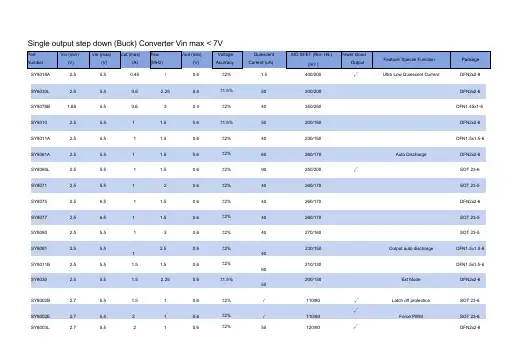
Single output step down (Buck) Converter Vin max < 7VSY8018A 2.5 5.5 0.45 / 0.6 ±2% 1.5 400/200 √Ultra Low Quiescent Current DFN2x2-8 SY8030L 2.5 5.5 0.6 2.25 0.6 ±1.5% 50 300/200 DFN2x2-6 SY8078B 1.85 5.5 0.6 3 0.4 ±2% 40 350/250 DFN1.45x1-6 SY8010 2.5 5.5 1 1.5 0.6 ±1.5% 50 200/150 DFN2x2-6 SY8011A 2.5 5.5 1 1.5 0.6 ±2% 40 230/150 DFN1.5x1.5-6 SY8061A 2.5 5.5 1 1.5 0.6 ±2% 60 260/170 Auto Discharge DFN2x2-6 SY8065L 2.5 5.5 1 1.5 0.6 ±2% 90 250/200 √SOT 23-6 SY8071 2.5 5.5 1 2 0.6 ±2% 40 260/170 SOT 23-5 SY8075 2.5 6.5 1 1.5 0.6 ±2% 40 260/170 DFN2x2-6 SY8077 2.5 6.5 1 1.5 0.6 ±2% 40 260/170 SOT 23-5 SY8080 2.5 5.5 1 3 0.6 ±2% 40 270/160 SOT 23-5SY8081 2.5 5.51 2.5 0.6 ±2%40230/150 Output auto discharge DFN1.5×1.5-6SY8011B 2.5 5.5 1.5 1.5 0.6 ±2%60210/130 DFN1.5x1.5-6SY8030 2.5 5.5 1.5 2.25 0.6 ±1.5%50200/150 Ext Mode DFN2x2-6 SY8002B 2.7 5.5 1.5 1 0.6 ±2% / 110/80 √Latch off protection SOT 23-6SY8002E 2.7 5.5 2 1 0.6 ±2% / 110/80 √Force PWM SOT 23-6SY8003L 2.7 5.5 2 1 0.6 ±2% 55 120/90 √DFN2x2-8Single output step down (Buck) Converter Vin max < 7V±2%SY8089 SOT 23-52.7 5.5 2 1 0.6 55 110/80 Latch off protectionSY8003C1 2.7 5.5 3 3 0.6 ±2% 55 110/80 √DFN2x2-8SY8823 2.5 5.5 3.5 2 0.6 ±1.5% 18 55/35 √QFN2x1.5-8SY8047 2.5 5.54 1.25 0.6 ±1.5%1875/55√QFN3x3-16SY8856 2.7 5.54 3 0.6 ±1.5%6035/15 √√DFN2x2-8√±1.5%SY8003F 2.7 5.5 3 1 0.6 / 110/80 DFN2x2-8 SY8079P 2.7 6.5 0.6 ±2% 55 125/95 Non latch off OVP SOT 23-6SY8032 2.7 5.5 2.5 0.6 ±2% 80 100/80 SOT 23-6SY8032E 2.7 5.5 2.5 0.6 ±2% 100/80 Force CCM SOT 23-6SY8003 2.7 5.5 0.6 ±2% 55 110/80 Latch SCP/OVP DFN2x2-8SY8003A 2.7 5.5 0.6 ±2% 55 110/80 Non-latch off protection DFN2x2-8SY8003C 2.7 5.5 0.6 ±2% 55 100/80 DFN2x2-8 SY8003E 2.7 5.5 0.6 ±2% 110/80 Force CCM DFN2x2-8 SY8043A 2.7 5.5 1.25 0.6 ±2% 18 75/55 DFN3x3-16 SY8047L 2.5 5.5 1.25 0.6 ±2% 18 75/55 QFN3x3-16 SY8859 2.7 5.5 0.6 ±1% 40 100/50 OVP/OCP/SCP/UVLO/OTP QFN1.5x1.5-7Single output step down (Buck) Converter Vin max < 7VPart Number Vin (min)(V)Vin (max)(V)Iout (max) (A) Fsw (MHz)Vout (min)( V)VoltageAcurracySY8824B 2.6 5.5 4 1.8 / ±1% SY8824C 2.6 5.5 4 1.8 / ±1% SY8035 2.7 5.5 5 1 0.6 ±1.5% SY8805A 3 5.5 5 1 0.6 ±1.5% SY8825 2.5 5.5 5 2 0.6 ±1.5% SY8876 2.7 6.5 6 1.2 0.6 ±1.5% SY8827K 2.5 5.5 6 2.4 ±1.5% SY8868 2.7 5.56 10.6 ±1% SY8099 2.7 5.5 6 1 0.6 ±1% SY8812 2.75 5.5 12 1 ±1%80 70/40Programmable Output Voltage: 0.7625Vto 1.55V in 12.5mV/step; Default 1.15Voutput voltage8015010018606550408070/4050/4035/1555/3538/1528/1735/1530/1212/6PackageTSOT 23-8Programmable Output Voltage: 0.7625Vto 1.55V in 12.5mV steps; Default 1.05Voutput voltageTSOT 23-8EXT SS DFN3x3-10DFN2x2-8QFN2x1.5-8OCP/UVLO/OTP DFN2x2-8I2C Programmable Vout: 0.7125V~ 1.5V CSP1.56x1.96-20in 12.5mV steps, Addr: 1000001xCOT mode,max dutyHigh efficiencyP rogrammable Output Voltage: 0.6V to1.5V in 10mV stepsQFN2x2-10TSOT 23-6QFN3x3-12Dual output step down (Buck) Converter Vin max < 7VPart Number Vin(min)(V)Vin(max)(V)Iout(max)(A)Fsw (MHz) Vout (min)(V)VoltageAcurracyQuiescentCurrent(uA)MO SFET Ron H/L (m? ) Power GoodOutputFeature/ Special Function PackageSY8020 2.5 5.5 1A x2 1.5 0.6 ±2% 50 200/150 Individual EN DFN3x3-12 SY8831 2.5 5.5 1A x2 1.5 0.6 ±2% 45/55 260/180 Individual EN TSOT 23-8 SY8832 2.5 5.5 2A x2 2 0.6 ±2% 35/45 125/100 Individual EN TSOT 23-8 SY8024 3 5.5 3A x2 1 0.6 ±2% 80 105/85 Individual EN DFN3x3-12 SY8821 2.5 5.5 1A/1.5A 2 0.6 ±2% 45 125/100 Individual EN DFN2x1.5-8Single output step down (Buck) Converter, Vin max > 7VuiescentOriginal Part Number Vin(min)(V)Vin(max)(V)Iout(max)(A)Fsw (MHz) Vout( imn)(V)Fixed O utputVoltage(V)VoltageAcurracyCurrent (uA)MOSFET(RonH/L) (m ? )Power oGodOutputFeature/ Special Function PackageSY8290 5 40 0.3 2 0.6 ±2.0% 160 2000/- SOT 23-6 SY8200 6 24 0.6 0.5 0.6 ±2% 400 420/200 SOT 23-6 SY8401 4.5 50 0.8 1.2 0.6 ±1.0% 150 700/- SOT 23-6SY8201 4.527 1 0.5 0.6 ±2%400350/150 SOT 23-6SY8201C 4.527 1 1.15 0.6 ±2%400350/150 Force CCM SOT 23-6SY85017 100 1 0.2~1MHz 1.2 ±2.0%400500/240 Programmable Switching Frequency SO8ESY8291 5 40 1.2 0.8 0.6 ±2.0% 160 180/- SOT 23-6 SY8502 7 100 1.8 0.2~1MHz 1.2 ±2.0% 400 500/240 Programmable Switching Frequency SO8ESingle output step down (Buck) Converter, Vin max > 7VVin(min) Vin(max) Iout(max) Fsw Vout(min) Voltage Quiescent MO SFET(Ron Power GoodPart Number(V) (V) Iout((m A)ax)(MHz) (V) Acurracy Current (uA) H/L) (m ? ) O utputFeature/ Special Function PackageSY8121 4.5 18 2 1 0.6 ±2% 400 170/160 SOT 23-6/ DFN2x2-6 SY8121B 4.35 18 2 1.2 0.6 ±2% 170/160 1.2MHz, FCCM SOT 23-6SY8120B1 4.5 18 2 0.5 0.6 ±2% 400 130/120 SOT 23-6SY8121C 4.5 18 2 1.2 0.6 ±2% 400 130/120 SOT 23-6SY8222 4.5 23 2 0.5 0.6 ±1.5% 400 150/110 √EXT SS, Hic-cup SCP DFN3x3-10SY8292 5 40 2 0.8 0.6 ±2.0% 160 180/- SOT 23-6SY8113B 4.5 18 3 0.5 0.6 ±1.5% 100 80/40 Hic-cup SCP TSOT 23-6SY8113C 4.518 3 1 0.6 ±1.5%10080/40 Hic-cup SCP TSOT 23-6SY8113D 4.5 18 3 0.5 0.6 ±1.5% 100 80/40 √Hic-cup SCP, EXT SS TSOT 23-8SY8113G 4.518 3 0.5 0.6 ±1.5%10080/40 Hic-cup SCP, FCCM TSOT 23-6SY8203A 4.523 3 1 0.6 ±1.5%400120/85 √EXT SS DFN3x3-10SY8223 4.523 3 0.5 0.6 ±1.5%400120/85 √EXT SS, Hic-cup SCP DFN3x3-10SY8253 4.5 23 3 0.5 0.6 ±1.5% 100 105/50 √EXT SS, Hic-cup SCP TSOT 23-8SY8303 4.5 40 3 0.5~2.5MHz 0.6 ±1.5% 18 70/110 TSOT 23-8 SY8293 5 40 3 0.8 0.6 ±2.0% 160 180/-SO8EPart Number Vin(min)(V)Vin(max)(V)Iout(max)(A)Fsw (MHz) Vout(min)(V)VoltageAcurracyQuiescentCurrent (uA)MO SFET(Ron H/L)(m ? )Power Good OutputFeature/ Special Function PackageSY8502 7 85 1.2 0.2~0.5 1.2 ±2.0% / 500/240 Programmable Switching FrequencyRangeSO8ESY8120B1 4.5 18 2 0.5 0.6 ±2% 400 130/120 SOT 23-6SY8121 4.5 18 2 1 0.6 ±2% 400 170/160 SOT 23-6/ DFN2x2-6 SY8121C 4.5 18 2 1.2 0.6 ±2% 400 130/120 SOT 23-6SY8222 4.5 23 2 0.5 0.6 ±1.5% 400 150/110 √EXT SS, Hic-cup SCP DFN3x3-10SY8292 5 40 2 0.8 0.6 ±2.0% 160 180/- SOT 23-6SY8113B 4.5 18 3 0.5 0.6 ±1.5% 100 80/40 Hic-cup SCP TSOT 23-6SY8113C 4.5 18 3 1 0.6 ±1.5% 100 80/40 Hic-cup SCP TSOT 23-6SY8113D 4.5 18 3 0.5 0.6 ±1.5% 100 80/40 √Hic-cup SCP, EXT SS TSOT 23-8SY8113G 4.5 18 3 0.5 0.6 ±1.5% 100 80/40 Hic-cup SCP, FCCM TSOT 23-6SY8203A 4.5 23 3 1 0.6 ±1.5% 400 120/85 √EXT SS DFN3x3-10SY8223 4.5 23 3 0.5 0.6 ±1.5% 400 120/85 √EXT SS, Hic-cup SCP DFN3x3-10SY8253 4.523 3 0.5 0.6 ±1.5%100105/50 √EXT SS, Hic-cup SCP TSOT 23-8SY8303 4.5 40 3 0.5~2.5MHz 0.6 ±1.5% 18 70/110 TSOT 23-8SY82935 40 3 0.8 0.6 ±2.0%160180/- SO8ESY8113H 4.5 18 3 0.5 0.6 ±1.5% 160 80/40 Programmable soft-start time TSOT 23-8±1.5%SY8104A4.518 4 0.5 0.6±1.5%100 50/30Instant PWM architectureSY8105 4.5 18 5 0.5 0.6±1.5%100 50/30SY8205 4.5 30 5 0.5 0.6±1.5%200 70/40√EXT SSSY8105A 4.5 18 5 0.5 0.6±1.5%100 40/20Instant PWM architectureSY8366H 4 28 6 0.8 0.6±1.5%100 40/20√Hic-cup SCP, 12A Peak current capability,programmable output current limitSY8286A 4 23 60.6 0.6 ±1.0% 12038/19 √SY8366K428 6 0.50.6±1.5%10040/20√Hic-cup SCP,6A continuous/12A peakoutput current capabilitySY8368A42880.80.6±1%100 20/10√Hic-cup SCP, 16A Peak current capability,programmable output current limitSY8288A 4 23 8 0.5 0.6 ±1.0% 80 30/10SY8288 4 23 8 0.5 0.6 ±1.0%8030/10SY8288C5.52380.60.6±1.5%10822/11√OVP/OCPSY8210A 4 28 10 0.6 0.6±1.5%300 25/8√Mem o ry power, 10A VDDQ/1A VTT LDO, 16A Peak Current capability, Latch offUVP/OVP, Over temperature alertSY8204 4.5 30 40.50.620080/50EXT SSPackageTSOT 23-6SO8ETSOT 23-6TSOT 23-6DFN3x4-12TSOT 23-6QFN3x3-12QFN3x3-20QFN3x3-12QFN3x3-12QFN3x3-20 QFN3x3-20QFN3x3-20QFN4x3-19Part Number Vin(min)(V)Vin(max)(V)Iout(max)(A)Fsw (MHz) Vout(min)(V) Voltage AcurracyQuiescent Current (uA)MO SFET(Ron H/L) (m ? ) Power Good OutputFeature/ Special Function Package SY8182 4 18 12 0.2~1MHz 0.6 ±1.0%18/6 √QFN4x4-20SY8182L 4.5 18 12 0.2~1MHz0.6 ±1.0% 500 18/6 √ Hic-cup SCP/OVPQFN4x4-24 SY8186418160.50.6±1.5%1507.5/2.5√Hic-cup SCP, programmble outputQFN4x4-11current limitPart NumberVin(min)(V)Vin(max)(V)Ilim (A)Fsw (MHz)Vout(max)(V)Sync BoostFixed O utputVoltage (V) Acu F r B ra /c y AcurracyInput Q uiescent Current (uA)Q uiescent current from output (uA)MO SFET Ro n (L/S) (m ? )Feature/ Special Function PackageSY7060L 0.7 5 0.2 / 5.25 Y /0.5V ±3% 0.518450/800SOT-363SY7070 0.7 5 0.35 / / Y 3.3 /0.5 5.5 500/700Bypass function @ shutdown SOT 23-5SY7070A 0.7 5 0.35 / / Y 3 / 0.5 5.5 500/700SOT 23-5SY7071 0.7 5 0.35 / 5.25 Y /1.0V ±3%0.5 5 500/700 Pass-through function @ shutdown SOT-363SY7071A 0.7 5 0.35 / / Y 5 / 0.5 7 400/500Pass-through function @ shutdown SOT-363SY7060 0.7 5 0.4 / 5.25 Y /0.5V ±3% 0.5 18 450/800SOT-363SY7080 0.9 4 1.8 1.2 4 Y / 1.2V ±3%65 / 90/200 Output Disconnect @Shutdown SOT 23-6Single output step Up (Boost) Converter (Low V oltage)Part NumberVin(min)(V)Vin(max)(V)Ilim (A)Fsw (MHz)Vout(max)(V)Sync BoostFixed O utput Voltage (V)Acu F rr B a /c y Acurracy InputQuiescent Current (uA) Quies cent current from output (uA) MOSFET Ron(L/S) (m ?) Feature/ Special Function PackageSY7063 1.8 5.25 3 0.5 5.5 Y / 1.2V ±1.5% 102736/40Output Disconnect @Shutdown QFN2x2-10SY7069 2.5 5.5 3 1 5.5 Y / 1.2V±1.5% 8 32 50/90TSOT 23-6SY7088 2.3 5 3 1 5.5 Y / 1.2V ±1.5% 2 30 70/85DFN2x3-8SY7088E 2.3 5 3 1 5.5 Y / 1.2V ±1.5% / / 70/85DFN2x3-8SY7065 1.8 5.25 5 0.5 5.5 Y / 1.2V ±1.5% 10 27 20/40 Auto output discharge function QFN2x2-10SY7065A 1.8 5.25 5 0.5 5.5 Y / 1.2V ±1.5% 10 27 20/40No output discharge function QFN2x2-10SY7076 2 5.5 6 0.5 5.5 Y / 1.2V ±1.5% 10 27 20/40QFN2x2-10SY7066 1.8 5.25 6 0.5 5.5 Y / 1.2V ±1.5% 10 27 20/40 Auto output discharge function QFN2x2-10SY7066B 1.8 5.25 6 0.5 5.5 Y / 1.2V ±1.5%10 27 20/40 Selectable Forced PWM mode QFN2x2-10Single output step Up (Boost) Converter (Low V oltage)SY9701A 2.6 5.5 1.2 1 5.5 0.6V ±1.5% 60 100/100 Output Disconnect @Shutdown DFN3x3-14Single output step Up (Boost) Converter (High Voltage)PackagePart NumberVin(min)(V)Vin(max)(V)Ilim (A)Fsw (MHz) Vout (max) (V) Sync BoostFB/ AcurracyInput Q uiescent Current (uA) MO SFET (RonMain/Rectified)(m? )Disconnect FET Ron ( m ?) Power Good OutputFeature/ Special FunctionSY7208C 3 25 0.6 1 25 N0.6V ±2%100 150/-Int SS/CompSOT 23-6SY7152A 3 8 2 1 16 N0.6V ±2%100 130/-Int SS/Comp SOT 23-6SY7208L 3 25 2 1 25 N0.6V ±2%100 150/-Int SS/Comp SOT 23-6SY7302 3 33 2 1 33 N0.6V ±2% 100 200/-Int SS/Comp SOT 23-6SY7388 3.5 30 2 0.85 30 N 1V ±2%150 200/-Accurate input current limit SOT 23-6SY7102 2 6 2.5 1 6 N0.6V ±2% 200 120/-Int SS/Comp SOT 23-6SY7801 2.5 5.5 2.5 1 / N 0.6V ±2%200 120/-Int SS, with 2A 80m? Load Switch DFN3x3-12SY7104A2 6 4 1 6 N0.6V ±2% 100 90/-Int SS/Comp DFN3x3-10SY7304 3334133N 0.6V ±2%100120/-QFN3x3-10SY7205 8.6 15.9 4.5 0.5 16 N1.25V±1.5% 120 75/-Adjustable soft-start time, OVP DFN3x3-10SY7982 3 9 6 1 13 Y 1V ±2% 600 80/4040√True shutdown QFN3x3-16SY7219 3 5.5 9 / 36 N 1.25V ±2%350 65/-EXT Comp DFN3x3-10 SY721531615/18Y1V ±1.5% 22016/1818√Int SS, OVP/SCP/ True shutdown ProgrammableSwitching Frequency: 0.2~1MHz QFN4x4-18SY7215A31615/18Y 1V ±1.5%2309/1212√Int SS, OVP/SCP/ True shutdown ProgrammableSwitching Frequency: 0.2~1MHzQFN4x4-181.23VInt SS; Adjustable current limit for optical module;SY7501B2.955.50.930.480N ±2%225 800/-Current limit indicator; Accurate high-side currentQFN3x3-16monitor; 320mW maximum output powerDC-DC PWM Controller (external Switch)Original Part Number Vin(min)(V)Vin(max)(V)Fsw (MHz)V(V R)EFFunction PackageSY7901 3 25 0.5 1 Current mode DC/DC controller targeted for Boost, Sepic, Flyback and Forward applications with DC Input Current Limit DFN3x3-10 SY7902A 3 25 0.3 1 Current mode DC/DC controller targeted for both Boost and Sepic applications with DC Output Current Limit SOP10 Power ModulePart Number Vin(min)(V)Vin(max)(V)Iout(max)(A)Fsw (MHz)Fixed O utputVoltage (V)Voltage Acurracy Q uiescent Current (uA) MOSFET (Ron H/L) (m? ) Integrated Inductor PackageSY98081 2.5 5.5 0.6 3 ±2% 40 230/150 √QFN2x1.5-8 SY98001 2.5 5.5 1.2 3 ±2% 40 230/150 √QFN2.5x2-8 SY98003 2.7 5.5 3 3 ±1.5% 60 35/15 √QFN3x3-10 SY98004 2.7 5.5 4 3 ±1.5% 60 35/15 √QFN3x3-10 SY98002 2.7 5.5 2 3 ±1.5% 60 20/40 √QFN3x3-10 SY98202 4.5 23 2 2 ±1.5% 100 50/105 √QFN3x3-10 SY98195 4.5 18 5 1.5 ±1.5% 15/50 √QFN5x5-20LDO RegulatorPart Number Vin(min)(V)Vin(max)(V)Vout(V)Iout(A)Dropout Voltage (mV) Function PackageSY6340 2.3 30 Output Voltage Adjustable 0.15 300 LDO Reg SOT23-5D FN2×2-6 SY6340B 3.6 30 3.3 0.05 100 LDO Reg SOT 23-5SY6345 4 40 Adjustable 0.3 300 LDO Reg SOT 23-5SY6301 1.6 5.5 Output Voltage Adjustable 1 0.32V at I OUT =1A, V OUT =1.5V0.18V at I OUT =1A, V OUT =2.8VLDO Reg DFN3×3-6SY6307B 0.8 5.5 Output Voltage Adjustable 0.5 90 LDO Reg DFN1.2x1.2-6 Protection SwitchPart Number Package Enabl eLogic O CP O VP No. ofChannelsVin(V) Vout(V) Iout(A) Rds(on) TUV/CBCertificateULCertificateSpecial FunctionSY6280A SOT 23-5 H Y N 1 2.4~5.5 2.4~5.5 0.4~2 63m? Programmable current limit, reverse blockingSY6281A SOT 23-5 L Y N 1 2.4~5.5 2.4~5.5 0.4~2 63m? Programmable current limit, reverse blockingSY6288A SOT 23-5 H Y N 1 2.5~5.5 2.5~5.5 0.6 80m? √√Output discharge at shutdown Reverse Blocking,OCB indicatorSY6288B SOT 23-5 L Y N 1 2.5~5.5 2.5~5.5 0.6 80m? ? ? Output discharge at shutdown Reverse Blocking,OCB indicatorSY6811 CSP0.9x0.9-4 H N N 1 1.05~1.95 1.05~1.95 1 45m?@VIN=1.2V35m?@VIN=1.8V Auto output cap discharge function, utra low inputvoltageSY6819A SO8 H Y N 1 4.5~18 4.5~18 1.2 110m?@VIN=12V Programmable blanking t ime for DFF control, Default Off when EN ONSY6819 SO8 H Y Y 1 4.5~18 4.5~18 1.2 110m?@VIN=12V Programmable blanking t ime for DFF control,Default On when EN ONSY6288C20 SOT 23-5 H Y N 1 2.5~5.5 2.5~5.5 2 65m? ? ? Output discharge at shutdown Reverse Blocking,OCB indicatorSY6288D20 SOT 23-5 L Y N1 2.5~5.5 2.5~5.5265m? √√Output discharge at shutdown Reverse Blocking,OCB indicatorPart Number Package EnableLogicOCP OVPNo. ofChannelsVin(V) Vout(V) Iout(A) Rds(on)TUV/CBCertificateULCertificateSpecial FunctionSY6882A DFN2x2-8 H N Y 1 3~23 3~23 2 100m?Internal Fixed Over-Voltage Protection Threshold @7.1V, Thermal Shutdown Protection&Auto RecoverySY6882B DFN2x2-8 H N Y 1 3~23 3~23 2 100m? Programmable OVP Threshold Thermal Shutdown Protection& Auto RecoverySY6883 SOT 23-6 L N Y 1 3~23 3~23 2 100m? Programmable OVP Threshold Thermal Shutdown Protection& Auto RecoverSY6822 QFN2x2-10 L Y N 1 3~6.6 3~6 2 60m? Bidirectional Current Limit SwitchSY6288C7 SOT 23-5 H Y N 1 2.5~5.5 2.5~5.5 2.5 70m? √Output discharge at shutdown Reverse Blocking,OCB indicatorSY6288D7 SOT 23-5 L Y N 1 2.5~5.5 2.5~5.5 2.5 70m? √Output discharge at shutdown Reverse Blocking,OCB indicatorSY6288C5 MSOP8 H Y N 1 2.5~5.5 2.5~5.5 2.5 70m? √√Output discharge at shutdown Reverse Blocking,OCB indicatorSY6288D5 MSOP8 L Y N 1 2.5~5.5 2.5~5.5 2.5 70m? √√Output discharge at shutdown Reverse Blocking,OCB indicatorSY6288E1 SOT 23-5 H Y N 1 2.5~5.5 2.5~5.5 3 45m? √√Output discharge at shutdown Reverse Blocking,OCB indicatorSY6288E2 SOT 23-5 L Y N 1 2.5~5.5 2.5~5.5 3 45m? √√Output discharge at shutdown Reverse Blocking,OCB indicatorSY6288F1 SOT 23-6 H Y N 1 2.5~5.5 2.5~5.5 3 45m? √Output discharge at shutdown Reverse Blocking,OCB indicatorSY6288F2 SOT 23-6 L Y N 1 2.5~5.5 2.5~5.5 3 45m? √Output discharge at shutdown Reverse Blocking,OCB indicatorSY6283A DFN1.2×1.6-4 H Y N 1 2.5~5.5 2.5~5.5 3 60m? Output discharge at shutdown Reverse Blocking SY6283 DFN1.2×1.6-4 H Y N 1 2.5~5.5 2.5~5.5 3 60m? Reverse blocking output, ultra low input voltage SY6813 6 ball CSP H N N 1 1.2~5.5 1.2~5.5 3 22m? Auto output cap discharge functionPart Number Package EnableLogicOCP OVPNo. ofChannelsVin(V) Vout(V) Iout(A) Rds(on)TUV/CBCertificateULCertificateSpecial FunctionSY6288D20 SOT 23-5 L Y N 1 2.5~5.5 2.5~5.5 2 65m? √√Output discharge at shutdown Reverse Blocking,OCB indicatorSY6882A DFN2x2-8 H N Y 1 3~23 3~23 2 100m?Internal Fixed Over-Voltage Protection Threshold @7.1V, Thermal Shutdown Protection&Auto RecoverySY6882B DFN2x2-8 H N Y 1 3~23 3~23 2 100m? Programmable OVP Threshold Thermal Shutdown Protection& Auto RecoverySY6883 SOT 23-6 L N Y 1 3~23 3~23 2 100m? Programmable OVP Threshold Thermal Shutdown Protection& Auto RecoverSY6822 QFN2x2-10 L Y N 1 3~6.6 3~6 2 60m? Bidirectional Current Limit SwitchSY6288C7 SOT 23-5 H Y N 1 2.5~5.5 2.5~5.5 2.5 70m? √Output discharge at shutdown Reverse Blocking,OCB indicatorSY6288D7 SOT 23-5 L Y N 1 2.5~5.5 2.5~5.5 2.5 70m? √Output discharge at shutdown Reverse Blocking,OCB indicatorSY6288C5 MSOP8 H Y N 1 2.5~5.5 2.5~5.5 2.5 70m? √√Output discharge at shutdown Reverse Blocking,OCB indicatorSY6288D5 MSOP8 L Y N 1 2.5~5.5 2.5~5.5 2.5 70m? √√Output discharge at shutdown Reverse Blocking,OCB indicatorSY6288E1 SOT 23-5 H Y N 1 2.5~5.5 2.5~5.5 3 45m? √√Output discharge at shutdown Reverse Blocking,OCB indicatorSY6288E2 SOT 23-5 L Y N 1 2.5~5.5 2.5~5.5 3 45m? √√Output discharge at shutdown Reverse Blocking,OCB indicatorSY6283A DFN1.2× 1.6-4 H Y N 1 2.5~5.5 2.5~5.5 3 60m? Output discharge at shutdown Reverse Blocking SY6283 DFN1.2× 1.6-4 H Y N 1 2.5~5.5 2.5~5.5 3 60m? Reverse blocking output, ultra low input voltage SY6813 6 ball CSP H N N 1 1.2~5.5 1.2~5.5 3 22m? Auto output cap discharge functionPart Number Package EnableLogicOCP OVPNo. ofChannelsVin(V) Vout(V) Iout(A) Rds(on)TUV/CBCertificateULCertificateSpecial FunctionSY6823 DFN2x2-8 H N N 2 0.6~5.5 0.6~5.5 4 28m? Programmable turn-on delay& ramp-up time,integrated OTP SCPSY6818 CSP1.73x1.73-12 H N Y 1 2.5~30 2.5~20 5 R PWPT =53m? (typ) Programmable OVP with Integrated Reverse Blocking FET, acurrate current level indicatorSY6874 DFN3x3-10 H Y Y 1 2.5~30 2.5~14 4 50m? Programmable softstart¤t limit,3.3V/5V/12V selectable clamping outputSY6875A DFN3x3-10 H Y Y 1 2.5~30 2.5~14 5 40m? Programmable softstart¤t limit,3.3V/5V/12V selectable clamping outputSY6875C DFN3x3-10 H Y Y 1 2.5~30 2.5-14 5 40m? Programmable softstart¤t limit, 3.3V/5V/12V selectable clamping outputSY6875D DFN3x3-10 H Y Y 1 2.5~30 2.5-14 5 40m? Programmable softstart¤t limit, 3.3V/5V/9V selectable clamping outputSY6875F DFN3x3-10 H Y Y 1 2.5~30 2.5-14 5 50m? Programmable softstart¤t limit,3.3V/5V/12V selectable clamping outputSY6895A DFN3x3-10 H Y Y 1 2.5~12 2.5~6.5 5 40m? Fixed Current Limit, Prog.SS SY6895C DFN3x3-10 H Y Y 1 2.5~12 2.5~6.5 5 40m? Fixed Current Limit, Prog.SSSY6880C CSP1.8x2-12 H N Y 1 2.5~28 0~7 5A continous,8A peak38m?Fixed intenal OVP@6.8V, Reverse block, Surgeprotection up to 80VSY6880A CSP1.8x2-12 H N Y 1 2.5~28 0~7 5A continous,8A peak 38m?SY6829 CSP0.79x0.79-4 H N Y 1 2.5~6 0~7 1 96m? Precise clamping output voltageSwitching ChargerPart Number Function Vin (V)Max. ChargeCurrent (A)Fsw (MHz) Series Cells Cell Voltage Special Function PackageSY6903A Single-Cell Bi-directional Power Bank 4.5-5.5 2 0.5 Single Cell 4.2V adaptive current limit, 2.4A Boost QFN3x3-16 SY6923 Single-Cell with USB-OT G 4~6 1.55 3 Single Cell 3/5~4.44V Compliance with USB and USB OT G, MTK reference design CSP 1.93x2.05-20 SY6923D Single-Cell with USB-OT G 4~6 1.55 3 Single Cell 3.5~4.44V Compliance with USB and USB OTG CSP 1.93x2.05-20 SY6923D1 Single-Cell with USB-OT G 3.5- 4.44 1.25/1.55 3 Single Cell 4.2V Compliance with USB and USB OTG CSP 1.93x2.05-20SY6932 Multi-cell Charger Step Down Reg. 4~23 2 0.8 1-3 Cells 4.2VProg. Charge Current&Timer,Output Power PathManagementQFN4x4-16SY6952A Single-cell Charger Step Down Reg. 4~23 2 0.8 Single Cell 4.2V,4.35V Power Path Management and Adaptive Input Current Limit QFN4x4-16 SY6952C Single-cell Charger Step Down Reg. 4~23 2 0.8 Single Cell 4.2V, 4.35V Power Path Management and Adaptive Input Current Limit DFN3x3-12 SY6952B1 Single-cell Charger Step Down Reg. 4~23 2 0.8 Single Cell 4.1V, 4.4V Adaptive Input Current Limit SO8ESY6982C 2 cell Boost Li-Ion Baterry Charger 3.6~5.5 2 1 2 Cells 4.2V, 4.35V Prog. Charge Current&T imer,Adaptive Input Current Limit QFN3x3-16SY6982C1 2 cell Boost Li-Ion Baterry Charger 3.6~5.52 12 Cells 4.1V, 4.25V Prog. Charge Current&T imer,Adaptive Input Current Limit QFN3x3-16 SY6982D 2 cell Boost Li-Ion Baterry Charger 3.6~5.5 2 1 2 Cells 4.1V, 4.2V, 4.3V, 4.35V Prog. Charge Current&T imer,Adaptive Input Current Limit QFN3x3-16SY6982E2 cell Boost Li-Ion Baterry Charger 3.6~5.52 12 Cells 4.2V, 4.35VProg. Charge Current&T imer,Adaptive Input Current LimitQFN3x3-16SY6982E12 cell Boost Li-Ion Baterry Charger 3.6~5.52 12 Cells 4.25V, 4.4VProg. Charge Current&T imer,Adapter and BAT IN IndicatorQFN3x3-16SY6982F 2 cell Boost Li-Ion Baterry Charger 3~5.5 2 1 2 Cells 4.2V Prog. Charge Current&T imer,Adapter and BAT IN Indicator QFN3x3-16 SY6903 Single-Cell Bi-directional Power Bank 4.5~5.35 2 0.5 Single Cell 4.2V 3in1, Adaptive current limit, 2.4A Boost QFN3x3-16 SY6903B Single-Cell Bi-directional Power Bank 4.5~5.3520.5 Single Cell 4.35V 3in1, Adaptive current limit, 2.4A Boost QFN3x3-16Part Number Function Vin (V)Max. ChargeCurrent (A)Fsw (MHz) Series Cells Cell Voltage Special Function PackageSY6908 Single-Cell Bi-directional Power Bank 4.5~5.35 2 0.5 Single Cell 4.2V 3in1, Adaptive current limit, 2.5A Boost QFN3x3-16SY6908A Single-Cell Bi-directional Power Bank 4.5~5.5 2 0.5 Single Cell 4.2V 3in1, Adaptive current limit, 2.5A Boost QFN3x3-16 SY6908B Single-Cell Bi-directional Power Bank 4.5~5.35 2 0.5 Single Cell 4.35V 3in1, Adaptive current limit, 2.5A Boost QFN3x3-16 SY6908D Single-Cell Bi-directional Power Bank 4.5~5.35 2 0.5 Single Cell 4.2V 3in1, Adaptive current limit, >10000mAH BAT, 2.5A Boost QFN3x3-16 SY6908E Single-Cell Bi-directional Power Bank 4.5~5.35 2 0.5 Single Cell 4.35V 3in1, Adaptive current limit, >10000mAH BAT, 2.5A Boost QFN3x3-16 SY6918 Single-Cell Bi-directional Power Bank 4.5~5.35 2 0.5 Single Cell 4.2V,4.35V Prog. current limit, 18V input voltage surge QFN3x3-16 SY6918A Single-Cell Bi-directional Power Bank 4.5~5.35 2 0.5 Single Cell 4.2V,4.35V Prog. current limit, 18V input voltage surge QFN3x3-16SY6918B Single-Cell Bi-directional Power Bank 4.5-5.3520.5 Single Cell 4.2V, 4.35V Prog. current limit, 18V input voltage surge QFN3x3-16SY6990 Single-Cell Bi-directional Power Bank 4~13.5 5 0.5 Single Cell 4.1V,4.2V,4.25V,4.4VI2C controlled, USB Complianced, 5V/3A&12V/1.2A Boost QFN4x4-24SY6992 Single-Cell Bi-directional Power Bank 4~13.5 5 0.5, 0.3 Single Cell 4.1V,4.2V,4.25V,4.4V I2C controlled, USB Complianced, 5V/4A&12V/1.5A Boost QFN4x4-20SY6993 Single-Cell Bi-directional Power Bank 4~13.5 5 0.5, 0.3 Single Cell 4.1V,4.2V,4.25V,4.4VI2C controlled, USB Complianced, 5V/4A&12V/1.5A Boost QFN4x4-20 SY6935 High Current Step-down Charger 4~14 3.5 1 1-2 Cells 4.2V, 4.35V Adaptive input current limit, Blocking FET integrated QFN3x3-16 SY7994 Synchronous Boost converter with QC3.0 3~4.5 NA 0.3, 0.5 Single Cell NA QC3.0 Compliance QFN4x4-20Power Management I CsPart Number Vin(min)(V)Vin(max)(V)Num ber ofChannelsPackage Application Integrated FunctionSY8675 9.3 18 3 SO8E TV power system 1 synchronous buck, 1 sy cnh ronous buck, 1 load switchSY8670 8 25 6 QFN5X5-32 TV Power System 4-Channel Step-Down onCve rter, 2-Channel LDOSY8632A 4.5 18 3 QFN5x5-32 TCON Power System I2C controlled 3-channel Buck RegulatorsSY6401A 4 18 1 DFN3x3-10 SSD Programmable charging current Automatic bi-directional energy flowSY6402 2.7 16 1 QFN3x4-19 SSD Input-side current limit switch Bi-directional DC-DC Regulator wit disconnhe ct switch: Boost Charging Mode and Buck Discharging Mode SY8645 3.4 5.5 8 QFN5x5-32 POS 4 Buck Converter, 2 LDO, one MOS switch, one load switch&one voltage detector.SY7630 2.5 5.5 3 QFN4x4-24 Monitor/NB LCD Panel Power AVDD Boost, VGH/VGL charge pump, VCOM OPAMP, GPMSY7630B 2.3 5.5 3 QFN4x4-24 Monitor/NB LCD Panel Power AVDD Boost, VGH/VGL charge pump, VCOM OPAMP, GPMSY8671 9.1 14.7 6 QFN6X6-40 TV LCD Panel Power 1 AVDD Boost, 1 HAVDD Buck, 2 Buck, 1 VON Boost, 1 VOFF Buck-BoostSY8673 8 18 5 QFN7x7-48 TV LCD Panel Power AVDD Boost, VGH/VGL charge pump, VCOM OPAMP, GPM, DVDD, Gammar reference LDOSY7615 8 18 2 DFN3x3-10 wer supply and control for satellite set t Boost, LNB BlogSY7615A8 18 2 DFN3x3-10 LNB power supply and control for s at elliteset top boxesBoost, LNB BlogSY8631 2.5 5.5 6 QFN4x4-24 Camera module Step Down Buck Regulators,3 Low Dropout LDO and 1 Channel RESET OutputSY86304 20 3DFN3x3-12 Security CCD Camera power supply 2 Buck converters and 1 Boost converterSY86412 5 5QFN3x3-16 3D Glass 1 Boost output with analog switches for 3D glassesSY8660C 2.7 5.5 1 DFN3x3-14 U SB Powered Devices Buck converter with programmable current limit switchSY8689 4.5 18 3 QFN4x4-24 TV Power/USB Ports and Hubs/Set-Top Dual synchronous buck regulator and an N-channel back-to-back power MOSFET switch。