
集成电路设计-part1-1
- 格式:ppt
- 大小:3.03 MB
- 文档页数:38


数字集成电路-电路系统与设计
数字电路设计的抽象层次:器件->电路->门->模块->系统
时钟偏差对全局信号都可能产⽣影响,是⾼性能⼤系统的设计关键。
集成电路的成本:固定成本+可变成本;固定成本可理解为研发成本,⾮重复的成本;可变成本可理解为⽣产制造(芯⽚成本和封测成本)过程中产⽣的成本,与良率也有关,控制芯⽚⾯积能够有效且直接的控制芯⽚成本。
⼀个门电路要想具有再⽣性,其VTC(电压传输特性)应当具有⼀个增益⼤于1的过渡区,以及增益⼩于1的合法区域,如下图:
封装可按照封装材料,互连层数量,散热⽅式进⾏分类:
封装材料:陶瓷封装、塑封(⾼分⼦聚合物) NMOS与PMOS,以增强型为例,NMOS VGS>Vth时导通,PMOS |VGS|>|Vth|时导通,且VGS<0。
CMOS反相器电压传输特性(VTC)推导:
上式为CMOS上下管需要遵守的规则。
结合上式得到,下图为CMOS中上官PMOS部分不同栅极输⼊电压下,下管NMOS电流与输出电压的关系
为了使NMOS和PMOS的传输特性能够符合上式DC成⽴,需要根据⼆者的V-I曲线找到交叉点,使其满⾜DC平衡
找到上图中的DC平衡交叉点,并提取绘制得到CMOS的电压传输特性如下图,可以看出CMOS的电压传输特性具有再⽣性
其中res表⽰呈电阻特性
PMOS和NMOS的电流⽅向问题:
源極的源是指載流⼦的起點;漏極的漏是指載流⼦的終點。載流⼦從源極出發,穿過溝道,到達漏極,從外部看,載流⼦最終從漏極漏出去了。顯然,NMOS和PMOS的載流⼦是不同的,因此導致了令⼈困惑的電流⽅向問題。盯住載流⼦即可,別被電流⽅向迷惑。
可以簡單地認為,柵極和襯底間的電壓超過閾值後,漏極和源極就接通了,⽽電流⼤⼩則是由柵漏源三極間的電壓決定。因為MOS是對稱結構,所以源極和漏極無區別且可互換。
關於D和S,也就是漏和源,其實是從⼯藝⾓度觀察的結果。在MOS中,有兩種載流⼦,⼀種是電⼦,另⼀種是空⽳,標記為N和P。顯然,NMOS的載流⼦是電⼦,PMOS的載流⼦是空⽳。NMOS導通後,電⼦從源極進⼊溝道,從漏極離開。因為電⼦的運動⽅向與電流⽅向相反,所以電流從NMOS的漏極流向源極。相反地,在PMOS中,雖然空⽳也是從源極進⼊溝道,從漏極離開,但空⽳的運動⽅向與電流⽅向⼀致。因此,電流從PMOS的源極流向漏極。CMOS中,通过上拉⽹络和下拉⽹络的互斥来保证静态下⽆直通电流,即上拉⽹络和下拉⽹络的导通状态总是相反。这意味着上拉⽹络和下拉⽹络存在对偶关系---串联对并联。
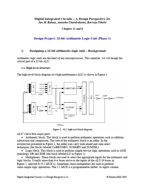
Digital Integrated Circuits―A Design Perspective 2/e © Prentice Hall 2003 Digital Integrated Circuits – A Design Perspective 2/e Jan M. Rabaey, Anantha Chandrakasan, Borivoje Nikolić Chapter 11 and 6 Design Project: 32-bit Arithmetic Logic Unit (Phase 1) 1. Designing a 32-bit atithmetic-logic unit – Background Arithmetic-logic units are the heart of any microprocessor. This semester, we will design the critical part of a 32-bit ALU. 1.1. High level structure The high-level block diagram of a high-performance ALU is shown in Figure 1. ALU’s have four major parts: • Arithmetic block: This block is used to perform arithmetic operations such as addition, subtraction and comparison. The core of the arithmetic block is an adder. In the architecture presented in Figure 1, the adder uses carry look-ahead and sum-select techniques (the blocks labeled CARRYGEN, SUMGEN and SUMSEL). • Logic block: This block is used to perform simple bitwise logic operations such as AND (masking), OR and XOR (the block labeled LU in Figure 1) • Multiplexers: These blocks are used to select the appropriate inputs for the arithmetic and logic blocks. Usually more than two buses arrive at the inputs of the ALU (9 buses in Figure 1, selected by 9:1 MUX’s). Sometimes these multiplexers are used to perform some simple logic operations. The 5:1 MUX is a programmable shifter: its inputs contain Digital Integrated Circuits―A Design Perspective 2/e © Prentice Hall 2003 shifted versions of the 9:1 MUX output. The 2:1 MUX can be programmed to invert one of the operands (this can be used to execute a subtraction using just an adder). • Registers: these blocks are used to store the operands and the results. Usually, these registers are not part of the microprocessor’s register file (though not always the case). Note that there is a bus looping from the output back to the input of the ALU, allowing it to use the newly computed results as operands in the next cycle. This is usually a very long wire (1.6mm in this case) and therefore puts a significant load on the previous stages. 2. Implementation and Constraints The goal of this project is to design the carry-lookahead adder for an ALU to be used in a high-performance or mobile microprocessor with a particular set of optimization criteria. The project will be completed in TWO phases. In the first phase of the project, you will choose a circuit style, design the logic, and lay out basic cells for a 32-bit adder. You will also have to do some pencil-and-paper optimization in order to meet the stated design goals and constraints. The complete adder will be assembled and simulated in PHASE 2. Physical and electrical specifications and constraints: 2.1. TECHNOLOGY: The design is to be implemented in a 0.25 µm CMOS process with 4 metal layers. The SPICE technology is in the g25.mod file. 2.2. POWER SUPPLY: You are free to choose any supply voltage and logic swing up to 2.5 V. Make sure that you use the appropriate model when you perform any hand analysis. 2.3. PERFORMANCE METRIC: The propagation delay for static CMOS design is defined as the time interval between the 50% transition point of the inputs and the 50% point of the worst-case output signal. Make sure you pick the worst-case condition and state EXPLICITLY in your report what that condition is. For dynamic designs, the propagation delay is defined in this case as the delays of the evaluate phase ONLY (at least in this phase of the project)! 2.4. AREA: The area is defined as the smallest rectangular box that can be drawn around the design. Since the ALU must interface with the cache, all of the row-matched inputs must be accessible from the left side of the design, in row-address order. In the first phase of the project, you should make area estimations based on the total transistor width and the wiring complexity. An expression for prediction of the area will be provided on the web page. 2.5. Each bit slice in the adder should accommodate 9 metal-5 busses and is 144λ (36 metal pitch) wide. Other circuits in the datapath set this constraint. 2.5. NAMING CONVENTIONS: The input operands of the adder are named A<31:0> and B<31:0>. The output is SUM<32:0>, where SUM<32> is the carry out bit. 2.6. REGISTERS: In this phase of the design, you do not need registers. The data flow from input to output should be combinational logic. 2.7. CLOCKS: There should be no global clock since the design is combinational. If you choose to use dynamic logic, you are permitted a precharge/evaluate clock, but the result must become available after ONE evaluate phase (no pipelined logic). Remember that the load capacitance of the clock should be included in the energy analysis. 2.8. VOH, VOL, NOISE MARGINS: You are free to choose your logic swing. The noise margins should be at least 10% of the voltage swing. Test this by computing the VTC between one of the inputs and the output signals (with the other outputs set to the appropriate values) for a static

集成电路版图设计 集成电路基本知识 集成电路按种类分类 模拟IC
数字IC
混合IC
集成电路按规模分类 SSI
MSI
LSI
VLSI
ULSI
GSI
集成电路设计流程 电路设计指标
芯片定义 电路图输入 线路拟真 版图 验证 寄生参数提取 芯片集成 芯片级验证寄生参数提取 后拟真
最终芯片导出 GDSII流片 PDK
CMOS集成电路工艺流程 剖面图 俯视效果,掩膜
工艺流程 氧化层生长
曝光 氧化层刻蚀
N阱注入 氮化硅刻蚀
场氧的生长 去除氮化硅
重新生长SIO2 生长多晶硅
刻蚀单晶硅 P离子注入
N离子注入 生长磷硅玻璃
光刻接触孔 刻铝
淀积钝化保护层
PDK 设计规则 width
space
enclosure
overlap
extension DRC、LVS、ERC 环境设置 数字标准单元库:APR IP库:成型的 工艺库:器件模型、拟真数据模型、pcell
到工艺库的根目录下解释各个子文件夹的作用 smic18mmrf:基础库
calibe:验证文件
drc,lvs
1p4m,一层poly,4层金属
model,spice_model,电路用的
n18指工作电压1.8v的管子
用一个管子来看层次
操作系统与Cadence软件 linux virtuoso spectre virtuoso schematic virtuoso layout
无源器件 电阻 种类 阱电阻
Poly电阻
原理
电容 种类 MIM电容
MOM电容
MOS电容
原理
电感 种类 电感
原理
有源器件 MOS 结构
原理
BJT 结构
原理
数字版图 基本数字单元标准化 面积最小化
布线最简化
实例 逻辑门
触发器 布局
布线
分频器 布局
布线
匹配方法 电阻 方案
画法
差分对 方案
画法
晶体三极管 方案
画法
电流镜 方案
画法
模拟版图 运算放大器 布局 差分对
电流镜
有源负载
电阻、电容
IC设计完整流程及工具
IC的设计过程可分为两个部分,分别为:前端设计(也称逻辑设计)和后
端设计(也称物理设计),这两个部分并没有统一严格的界限,凡涉及到与工艺
有关的设计可称为后端设计。
前端设计的主要流程:
1、规格制定
芯片规格,也就像功能列表一样,是客户向芯片设计公司(称为Fabless,
无晶圆设计公司)提出的设计要求,包括芯片需要达到的具体功能和性能方面的
要求。
2、详细设计
Fabless根据客户提出的规格要求,拿出设计解决方案和具体实现架构,划
分模块功能。
3、HDL编码
使用硬件描述语言(VHDL,VerilogHDL,业界公司一般都是使用后者)将
模块功能以代码来描述实现,也就是将实际的硬件电路功能通过HDL语言描述
出来,形成RTL(寄存器传输级)代码。
4、仿真验证
仿真验证就是检验编码设计的正确性,检验的标准就是第一步制定的规格。
看设计是否精确地满足了规格中的所有要求。规格是设计正确与否的黄金标准,
一切违反,不符合规格要求的,就需要重新修改设计和编码。设计和仿真验证是
反复迭代的过程,直到验证结果显示完全符合规格标准。仿真验证工具Mentor
公司的Modelsim,Synopsys的VCS,还有Cadence的NC-Verilog均可以对RTL
级的代码进行设计验证,该部分个人一般使用第一个-Modelsim。该部分称为前
仿真,接下来逻辑部分综合之后再一次进行的仿真可称为后仿真。
5、逻辑综合――DesignCompiler
仿真验证通过,进行逻辑综合。逻辑综合的结果就是把设计实现的HDL代
码翻译成门级网表netlist。综合需要设定约束条件,就是你希望综合出来的电路
在面积,时序等目标参数上达到的标准。逻辑综合需要基于特定的综合库,不同
的库中,门电路基本标准单元(standardcell)的面积,时序参数是不一样的。所
以,选用的综合库不一样,综合出来的电路在时序,面积上是有差异的。一般来
说,综合完成后需要再次做仿真验证(这个也称为后仿真,之前的称为前仿真)