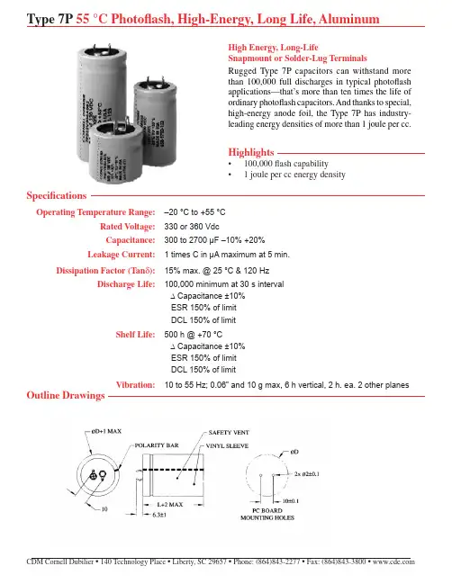
EPI330352AC3中文资料
- 格式:pdf
- 大小:90.16 KB
- 文档页数:1

Features■Support for numerous single-ended and differential I/O standards■High-speed differential I/O support with DPA circuitry for 1-Gbpsperformance■Support for high-speed networking and communications busstandards including Parallel RapidIO, SPI-4 Phase 2 (POS-PHYLevel4), HyperTransport™ technology, and SFI-4■Support for high-speed external memory, including DDR and DDR2SDRAM, RLDRAM II, QDR II SRAM, and SDR SDRAM■Support for multiple intellectual property megafunctions fromAltera MegaCore® functions and Altera Megafunction PartnersProgram (AMPP SM) megafunctions■Support for design security using configuration bitstreamencryption■Support for remote configuration updatesTable1–1. Stratix II FPGA Family FeaturesFeature EP2S15EP2S30EP2S60EP2S90EP2S130EP2S180 ALMs6,24013,55224,17636,38453,01671,760 Adaptive look-up tables (ALUTs) (1)12,48027,10448,35272,768106,032143,520 Equivalent LEs (2)15,60033,88060,44090,960132,540179,400 M512 RAM blocks104202329488699930M4K RAM blocks78144255408609768M-RAM blocks012469T otal RAM bits419,3281,369,7282,544,1924,520,4886,747,8409,383,040 DSP blocks12163648639618-bit × 18-bit multipliers (3)4864144192252384 Enhanced PLLs224444Fast PLLs448888 Maximum user I/O pins3665007189021,1261,170 Notes to Table1–1:(1)One ALM contains two ALUTs. The ALUT is the cell used in the Quartus®II software for logic synthesis.(2)This is the equivalent number of LEs in a Stratix device (four-input LUT-based architecture).(3)These multipliers are implemented using the DSP blocks.Stratix II Device Handbook, Volume 1Stratix II Architecture Figure2–53.Input Timing Diagram in DDR ModeWhen using the IOE for DDR outputs, the two output registers areconfigured to clock two data paths from ALMs on rising clock edges.These output registers are multiplexed by the clock to drive the outputpin at a ×2 rate. One output register clocks the first bit out on the clockhigh time, while the other output register clocks the second bit out on theclock low time. Figure2–54 shows the IOE configured for DDR output.Figure2–55 shows the DDR output timing diagram.Stratix II Device Handbook, Volume 1PLLs & Clock Networks1When using the global or regional clock control blocks inStratix II devices to select between multiple clocks or to enableand disable clock networks, be aware of possible narrow pulsesor glitches when switching from one clock signal to another. Aglitch or runt pulse has a width that is less than the width of thehighest frequency input clock signal. To prevent logic errorswithin the FPGA, Altera recommends that you build circuitsthat filter out glitches and runt pulses.Figures2–37 through 2–39 show the clock control block for the globalclock, regional clock, and PLL external clock output, respectively.Figure2–37.Global Clock Control BlocksNotes to Figure2–37:(1)These clock select signals can be dynamically controlled through internal logicwhen the device is operating in user mode.(2)These clock select signals can only be set through a configuration file (.sof or .pof)and cannot be dynamically controlled during user mode operation.Stratix II Device Handbook, Volume 1。