北京交通大学2014-2015数字电子技术期末考试试卷
- 格式:docx
- 大小:43.62 KB
- 文档页数:6
北京交通大学考试试题(A卷)课程名称:电子测量学年学期:2013-2014学年第1学期课程编号: 14L109Q-02 开课学院:电子学院出题教师:课程组学生姓名:学号:任课教师:学生学院:班级:(请考生注意:本试卷共有六道大题。
所有题答在答题纸上)一、选择题(单项选择题, 每题2分(除了标注*的为1分外),共30分)1.下面关于各种测量相关概念的描述中,哪一个是错误的:(A )。
(A)测量是认识自然界的主要工具,测量结果通常用一个确定的数值来表示。
(B)狭义地说,电子测量是通过运用电子科学的原理、方法和设备对各种电量、电信号及电路元器件的特性和参数进行测量。
(C)计量具有统一性、准确性和法制性的特点。
(D)计量基准或计量标准是指“为了定义、实现、保存或复现量的单位或一个或多个量值,用作参考的实物量具、测量仪器、参考物质或测量系统”。
2. 下面关于引用误差的描述中,哪一个是错误的:(C )(A )引用误差又称为满度相对误差或引用相对误差。
(B )引用误差是可正、可负的,通常用百分数表示。
(C )引用误差的定义是仪器示值的相对误差与测量范围上限值(量程)之比。
(D )如果一块电压表的等级为±1.0级,表明使用该电压表进行电压测量的最大引用误差不超过±1.0%。
3. 使用数字万用表测量某工频信号的电压,将多次测量测得的电压值用数轴上的实心圆点来表示,得到下面4个图,图中的空心圆点v 0表示用高等级数字万用表测量该信号电压的实际值,则下面4个图中测量正确度最差的是( C )。
4. 以下关于粗大误差及系统误差的判据描述中,错误的是:( D )(A )肖维纳检验法也是以正态分布作为前提的,且给出了剔除数据判据对应得置信概率。
(B )格拉布斯检验法是在未知总体标准偏差的情况下,对正态样本或接近正态样本异常值进行判别的一种方法。
(C )马利科夫判据是常用的判别有无累进性系统误差的方法。
当n 为偶数,如果以下不等式成立,则认为测量中存在累进性系统误差。
北京交通大学智慧树知到“电气工程及其自动化”《数字电子技术(含实验)》网课测试题答案(图片大小可自由调整)第1卷一.综合考核(共10题)1.设周期性数字波形的高电平持续6ms,低电平持续10ms,占空比为()。
A.60%B.47.5%C.37.5%D.30%2.0FEH是我们常用数制中的十六进制。
()A.错误B.正确3.数字系统设计分为自下而上和自上而下的设计方法。
()A.错误B.正确4.一个双稳态触发器可以保存1位二值信息。
()A.错误B.正确5.()构成各种时序电路的存储单元电路。
A.寄存器B.锁存器C.触发器D.定时器6.D码是用字母B、C、D、表示的代码。
()A.错误B.正确7.0FEH是数制中的十六进制。
() A.错误B.正确8.TTL电路在正逻辑系统中,以下各种输入中()相当于输入逻辑“1”。
A.悬空B.通过电阻2.7kΩ接电源C.通过电阻2.7kΩ接地D.通过电阻510Ω接地9.八进制数(18)8比十进制(18)10小。
()A.错误B.正确10.ASM图中有状态框、判断框、输出框三种符号。
()A.错误B.正确第1卷参考答案一.综合考核1.参考答案:C2.参考答案:B3.参考答案:B4.参考答案:B5.参考答案:BC6.参考答案:A7.参考答案:B8.参考答案:ABC9.参考答案:A10.参考答案:B。
北京理工大学2014-2015学年数据结构期末考试卷北京理工大学2014-2015学年第一学期《数据结构》期末考试试题(A)一、选择题(24分)1,下面关于线性表的叙述错误的是()。
(A)线性表采用顺序存储必须占用一片连续的存储空间(B)线性表采用链式存储不必占用一片连续的存储空间(C)线性表采用链式存储便于插入和删除操作的实现(D)线性表采用顺序存储便于插入和删除操作的实现2,设哈夫曼树中的叶子结点总数为m,若用二叉链表作为存储结构,则该哈夫曼树中总共有()个空指针域。
(A)2m-1(B)2m(C)2m+1(D)4m3,设顺序循环队列Q[0:M-1]的头指针和尾指针分别为F和R,头指针F总是指向队头元素的前一位置,尾指针R总是指向队尾元素的当前位置,则该循环队列中的元素个数为()(A)R-F(B)F-R(C)(R-F+M)%M(D)(F-R+M)%M4,设某棵二叉树的中序遍历序列为ABCD,前序遍历序列为CABD,则后序遍历该二叉树得到序列为()。
(A)BADC(B)BCDA(C)CDAB(D)CBDA5,设某完全无向图中有n个顶点,则该完全无向图中有()条边。
(A)n(n-1)/2(B)n(n-1)(C)n2(D)n2-1,6,设某棵二叉树中有2000个结点,则该二叉树的最小高度为()(А)9(B)10(C)11(D)127,设某有向图中有n个顶点,则该有向图对应的邻接表中有()个表头结点。
(A)n-1(B)n(C)n+1(D)2n-18,设一组初始记录关键字序列(5,2,6,3,8),以第一个记录关键字5为基准进行一趟快速排序的结果为()。
(A)2,3,5,8,6(B)3,2,5,8,6(C)3,2,5,6,8(D)2,3,6,5,8二、填空题(24 分)1,为了能有效地应用HASH查找技术,必须解决的两个问题是________________和________________________。
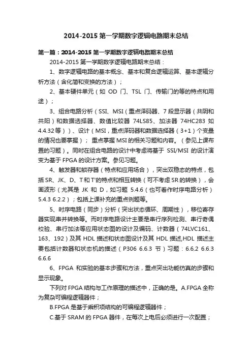
2014-2015第一学期数字逻辑电路期末总结第一篇:2014-2015第一学期数字逻辑电路期末总结2014-2015第一学期数字逻辑电路期末总结:1、数字逻辑电路的基本概念、基本和复合逻辑运算、基本逻辑分析方法(含化简和变换的方法);2、基本硬件单元(如OD门、TSL门、传输门的等的特点和用途);3、组合电路分析(SSI、MSI(重点译码器、7段显示器(共阴和共阳)和数据选择器、数值比较器74LS85、加法器74HC283 如4.4.32等))、设计(MSI,重点译码器和数据选择器(3+1)个变量的情况也要掌握);重点掌握MSI的相关习题和内容。
(参见上课布置的习题)。
同时在组合电路的设计中考虑将基于SSI/MSI的设计演变为基于FPGA的设计方案。
参见习题。
4、触发器和锁存器(特点和应用场合),突出双稳态的特点,包括SR、JK、D、T和T'的特点和相互转换(可不考虑SR的转换),会画波形(尤其是JK和D,如习题5.4.6(也可看作时序电路分析)5.4.3 6.2.2);包括上课补充的重点例题等。
5、时序电路(同步)分析(突出状态循环、周期性),移位寄存器实现串并转换等。
而时序电路设计主要是串行序列检测、串行奇偶校验、串行加法等应用状态图的设计及编码、计数器(74LVC161、163、192)及其HDL描述和状态图设计及其HDL描述,HDL 描述主要包括计数器和状态机的描述(P306 6.6.3节)习题:6.6.2 6.6.3 6.6.66、FPGA和实验的基本步骤和方法,重点突出功能仿真的步骤和显示现象。
下列对FPGA结构与工作原理的描述中,正确的是。
A.FPGA全称为复杂可编程逻辑器件;B.FPGA是基于乘积项结构的可编程逻辑器件;C.基于SRAM的FPGA器件,在每次上电后必须进行一次配置;D.FPGA更适合完成各种算法和组合逻辑, CPLD更适合于完成时序逻辑。
在VerilogHDL的always块中,阻塞式赋值语句和非阻塞赋值语句执行过程的主要区别是阻塞赋值语句是立即执行,非阻塞是多条费阻塞赋值语句运算结束时,才同时并行完成赋值语句。
西交《数字电子技术》在线作业试卷总分:100 测试时间:--单选题一、单选题(共50道试题,共100分。
)V1. _________ 处理的电子电路是数字电路。
A.交流电压信B.直流信号C.模拟信号D.数字信号满分:2分2. 用卡诺图化简具有无关项的逻辑函数时,若用圈1法,在包围圈内的’是按处理;在包围圈外的是按________ 处理。
r\A. 1,1gB. 1,0C. 0,0rjiD. 不确定。
满分:2分3.两个与非门构成的基本腊触发器,当Q二1、◎二0时,当两个输入信冲示=1和E=1器的输出Q会____________ aC A.变为0B.保持1不变rC.保持0不变rD.无法确定4. 10- 4线优先编码器允许同时输入路编码信号满分:2分4. 11- 4线优先编码器允许同时输入路编码信号OA. 0.3VB. 0.5VC. 0.8VA. 放大B. 饱和D. 开关满分:2分7. TTL 与非门输出低电平的参数规范值是A. UOL w 0.3VC. UOL w 0.4V满分:2分8. 三极管开关电路中,影响开关速度的主要因素是A. 1B. 9C. 10D.多满分:2 5.标准TTL 分门关门电平Uoff 之值为A. tdB. trCl D. 1.2V满分:26.数字电路中,晶体管的工作于 状态。
Cl C .截止B. UOL > 0.3VD. UOL= 0.8V12. 口 C. tsD. tf满分:2分9. TTL 与非门输出高电平的参数规范值是A. UOH > 1.4VB. UOH > 2.4VC. UOH > 3.3V口 D. UOH= 3.6V满分:2分10. 利用2个74LS138和1个非门,可以扩展得到A. 2-4「B. 3-8C. 4-16D. 无法确定。
满分:2分11. __________ 当 时,增强型NMOS 管相当于开关接通。
回>匚味0皿v 〔工A.B.C.满分:2分TTL 与非门高电平输入电溢治的参数规范值是[a) 20 pA (b)40pA(c> 1.6 mA (d) 16 mA线译码器。
北京交通大学考试试题(A卷)课程名称:微机原理与接口学年学期:2013—2014学年第1学期课程编号:14L128Q-03 开课学院:电信出题教师:5人学生:学号:任课教师:学生学院:班级:一、填空题(每题2分,共10分)1.80X86微机系统采用补码存储数据,16位补码表示的数值围为:____________________。
(-65536~+65535)2.某RAM芯片,其数据线为D0-D7,地址线为A0-A11,则此芯片的存储容量为:________。
(4KB )3.伪指令XBF DW 10 DUP(10,10 DUP(10)),系统为变量XBF 分配的字节数为:________。
(110)/6EH4.80X86微机系统根据中断向量表,获取中断向量,中断向量表的地址围为:__________。
(000H~3FFH)5.DMAC芯片8237A部有_______个独立的通道,每个通道的选址围为:_______。
4 64KB二、选择题(单选,每题2分,共10分)1.下列哪条指令执行后对状态标志位没有影响。
()AA. MOV AL,33HB. ADD AL,33HC. CMP AL,33HD. TEST AL,33H2.已知X1是定义的一个变量,下列哪条指令与LEA AX,X1结果相同。
()DA. MOV AX,X1B.ADD AX,X1C.MOV AX, SEG X1D. MOV AX, OFFSET X13.中断控制器8259中用于存放CPU当前正在服务的中断标志的寄存器为:()B A. 中断请求寄存器IRR B. 中断服务寄存器ISRC. 中断屏蔽寄存器IMRD. 中断优先权判别器PR4.串行接口芯片8250不能处理下列哪种中断。
()CA.接收数据出错 B. 接收缓冲器满C. 发送数据出错D. 发送寄存器空5.某微机系统含有3片8237A,其中一片为主片,两片为从片,试问此系统可以使用多少个DMA通道。

新乡学院2013-2014学年二学期课程考试试卷答案(A 卷)课程名称:电工学 考试时间:120分钟 年级:xxx 级专业: xxx题目部分,(卷面共有18题,100分,各大题标有题量和总分) 一、单项选择题(10小题,共24分)1、分析图示控制电路,当接通电源后其控制作用正确的是( )。
A 、按2SB ,接触器KM 通电动作;按1SB ,KM 断电恢复常态 B 、按着2SB ,KM 通电动作,松开2SB ,KM 即断电C 、按2SB ,KM 通电动作,按1SB ,不能使KM 断电恢复常态,除非切断电源KM2答案:C2、设功率放大电路的输出功率为P O ,电源供给该电路的功率为P E ,功率晶体管消耗的功率为P T ,则该放大电路的效率等于()。
A 、P P OTB 、P P O EC 、P P TE答案:B3、射极输出器是()。
A 、共集电极电路B 、共发射极电路C 、共基极电路答案:A4、运算放大器电路如图所示,输入电压2i u V ,则输出电压O u 等于()。
A 、2VB 、正饱和值C 、负饱和值-∞+答案:A5、电路如图所示,若i u 一定,当可变电阻P R 的电阻值由小适当增大时,则输出电压的变化情况为()。
A 、由小变大B 、由大变小C 、基本不变-∞+R 2答案:B6、电路如图所示,电位器P R 为10k Ω,若输入电压10i u V =,当电位器的移动点移至B 点时,则输出电压O u 为()。
A 、0VB 、2.5VC 、-15VD 、30V-∞+u O10k ΩΩ答案:B7、采用共阳极数码管的译码显示电路如图所示,若显示码数是1,译码器输出端应为()。
A 、"0","1","0"a b c d e f g =======B 、"1","0","0"a b c d e f g =======C 、"1","0","1"a b c d e f g =======ABC D答案:C8A 、B 、 答案:9、如图所示时序逻辑电路为()。
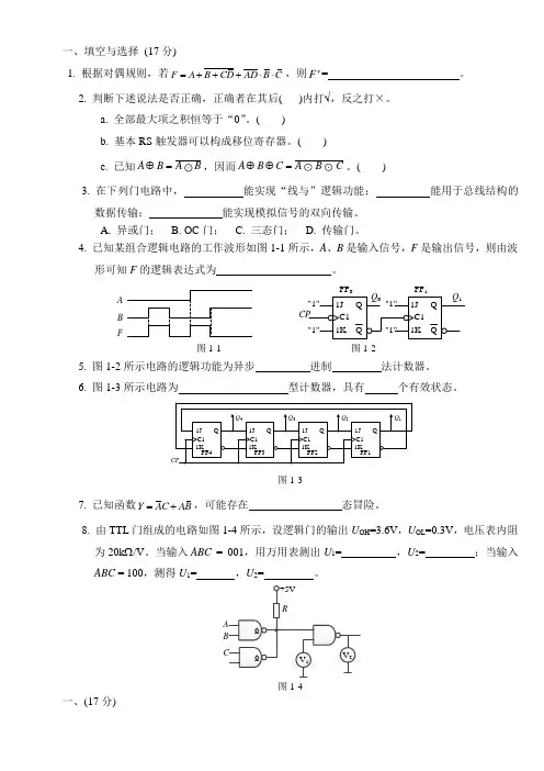
一、填空与选择 (17分)1. 根据对偶规则,若F A B CD AD B C =+++⋅⋅,则F '= 。
2. 判断下述说法是否正确,正确者在其后( )内打√,反之打×。
a. 全部最大项之积恒等于“0”。
( )b. 基本RS 触发器可以构成移位寄存器。
( )c. 已知A B AB ⊕=,因而A BC ABC ⊕⊕=。
( )3. 在下列门电路中, 能实现“线与”逻辑功能; 能用于总线结构的数据传输; 能实现模拟信号的双向传输。
A. 异或门; B. OC 门; C. 三态门; D. 传输门。
4. 已知某组合逻辑电路的工作波形如图1-1所示,A 、B 是输入信号,F 是输出信号,则由波 形可知F 的逻辑表达式为 。
B AF1J Q QC11K 1J Q QC11K CP Q 0Q 1FF 0FF 1"1""1""1""1"图1-1 图1-25. 图1-2所示电路的逻辑功能为异步 进制 法计数器。
6. 图1-3所示电路为 型计数器,具有 个有效状态。
图1-37. 已知函数Y AC AB =+,可能存在 态冒险。
8. 由TTL 门组成的电路如图1-4所示,设逻辑门的输出U OH =3.6V ,U OL =0.3V ,电压表内阻为20k Ω/V 。
当输入ABC = 001,用万用表测出U 1= ,U 2= ;当输入ABC = 100,测得U 1= ,U 2= 。
图1-4一、(17分)1. ()()F A B C D A D B C =⋅⋅+++++=()()A B C D A D B C AB ACD⋅⋅+⋅+++=+2. √,×,×3. B ,C ,D4. A B ⊕5. 二位二进制(四进制),减法6. 扭环,8个7. 08.0.3V , 3.6V; 1.4V , 0.3V;二、简答题:(8分)1. 电路如图2-1(a)所示,设各触发器的初态为“0”。
武汉大学2014—2015学年度第二学期《数字电子技术基础》试卷(A)学号姓名院(系)分数一、填空题,每空1分(共20分)1.逻辑函数有多种表达方式,其中的四种为(),(),()和()。
2、(25.7)10=()2=()16。
3、可以实现线与功能的逻辑门电路包括(),()和()。
4、JK触发器若J=K,则可实现()触发器的功能;若J=K,则可实现()触发器的功能。
5、5位环形和扭环形计数器,若初态均为10110(低位在左),则26个CP后环形计数器的并行输出为(),扭环计数器的并行输出为()。
6、128K×16的只读存储器,其寻址地址线数目是()根,字长是()位,字数是(),总容量是()。
7、可以实现更大规模逻辑电路的可编程器件主要包括()和()。
8、设四位D/A转换器的满刻度输出电压30V,则输入数字量是1011时的输出模拟电压为()V。
二、单项选择填空,每空2分(共20分)1、编码(11111100.11010100)2421对应的十进制数为()。
A.97.64B.86.54C.96.74D.85.742、逻辑函数F=A B C⨯+且BC=0的卡诺图中,最小项和无关项个数分别为()个。
A.4,2B.3,2C.3,3D.2,43、下列说法正确的共有()个。
(1)按制造门电路晶体管的不同,门电路可分为MOS型和双极型;(2)TTL电路相对CMOS电路的特点是速度快,但功耗大;(3)CMOS电路的静态功耗很小,主要是动态功耗;(4)TTL器件驱动CMOS器件主要需要校验灌电流是否满足要求;A.1B.2C.3D.44、已知题2.4图中的门电路是74系列的TTL门电路,则电路的输出电平是()。
A.高电平B.高阻C.低电平D.无法判断5、要将方波脉冲的周期扩展10倍,可采用()。
A.10级施密特触发器B.10位二进制计数器C.十进制计数器D.10位D/A转换器第1页共4页6、用4片4K×16的RAM构成4K×16的存储器,扩展后地址空间最高的一片4K×16的RAM的寻址范围是()。
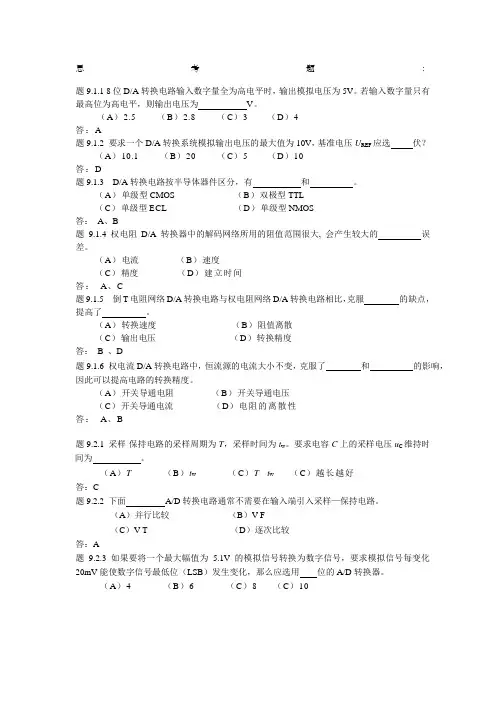
思考题:题9.1.1 8位D/A转换电路输入数字量全为高电平时,输出模拟电压为5V。
若输入数字量只有最高位为高电平,则输出电压为V。
(A)2.5 (B)2.8 (C)3(D)4答:A题9.1.2 要求一个D/A转换系统模拟输出电压的最大值为10V,基准电压U REF应选伏?(A)10.1 (B)20 (C)5(D)10答:D题9.1.3 D/A转换电路按半导体器件区分,有和。
(A)单级型CMOS (B)双极型TTL(C)单级型ECL(D)单级型NMOS答:A、B题9.1.4 权电阻D/A转换器中的解码网络所用的阻值范围很大, 会产生较大的误差。
(A)电流(B)速度(C)精度(D)建立时间答:A、C题9.1.5 倒T电阻网络D/A转换电路与权电阻网络D/A转换电路相比,克服的缺点,提高了。
(A)转换速度(B)阻值离散(C)输出电压(D)转换精度答:B 、D题9.1.6 权电流D/A转换电路中,恒流源的电流大小不变,克服了和的影响,因此可以提高电路的转换精度。
(A)开关导通电阻(B)开关导通电压(C)开关导通电流(D)电阻的离散性答:A、B题9.2.1 采样-保持电路的采样周期为T,采样时间为t w。
要求电容C上的采样电压u C维持时间为。
(A)T(B)t w(C)T - t w(C)越长越好答:C题9.2.2 下面A/D转换电路通常不需要在输入端引入采样—保持电路。
(A)并行比较(B)V-F(C)V-T (D)逐次比较答:A题9.2.3如果要将一个最大幅值为 5.1V的模拟信号转换为数字信号,要求模拟信号每变化20mV能使数字信号最低位(LSB)发生变化,那么应选用位的A/D转换器。
(A)4 (B)6 (C)8 (C)10答:C题9.2.4 速度最快的A/D转换电路是A/D转换电路。
(A)并行比较(B)串行比较(C)双积分(D)逐次比较答:A题9.2.5 衡量A/D转换电路的主要技术指标是和。
(A)偏移误差(B)转换精度(C)转换速度(D)分辨时间答:B、C题9.2.6 逐次比较型A/D转换电路加入固定负电压补偿电压电路的目的是。
北京交通大学考试试题A 课程名称:数字电子技术 2014—2015学年 第1学期 命题教师 集体 班级: 学号: 姓名: 题号 一 二 三 四 五 六 总分 得分 签字
I Concepts (20 points, 2 points/question) 1. of the following binary number is the two's complement representation of the decimal number 14? (A) 0000 1110 (B) 1111 0010 (C) 0111 1110 (D) 1000 1110 2. The speed of CMOS devices mainly depend on and . (A) Stray capacitance (B) Source voltage (C) Load resistance (D) Transistor resistance 3.For a CMOS circuit, of the following conditions has the largest power consumption. (A) Have large load resistance (B) Whose output is not changing (C) Have small external capacitances (D) Both of the PMOS and NMOS are on 4. The result of timing hazards is ?
(A) Cause unpredictable outputs (B) Produce a glitch (C) The output is unstable (D) Make the circuit get into metastability 5. Device is designed for transferring data from one of n sources to the output.
(A) Decoder (B) Encoder (C) Multiplexer (D) Three state buffer 6. will sample its input and change its output to the state of its input at the rising edge of a clock signal? (A) Edge-Triggered D Flip-Flop (B) Edge-Triggered J-K Flip-Flop (C) T Flip-Flop (D) Master/Slave J-K Flip-Flop 7.How to make digital systems deal with asynchronous input signals that are not synchronized with the system clock? (A)Change the clock frequency (B) Employ a D Flip-Flop as a synchronizer (C)Use a S-R latch to control the input (D) Add a combinational logic circuit 8.When the high-impedance output of a three-state device and a signal A is connected to the inputs of a TTL AND gate, the output will be . (A) 0 (B) 1 (C) signal A (D) Inverse of signal A 9. The original transition table of a sequential circuit is given in Table 1, it can be simplified into states. (A) 2 (B) 1 (C) 3 (D) 0 Table1 Transition table X Sn 0 1
S0 S1 S2 S3 S0/1 S1/0 S2/0 S2/0 S1/1 S2/0 S0/0 S0/0 Sn+1/F 10. Of the following memory types, and belong to the volatile memory type. (A) FPGA (B)EROM (C)SRAM (D) FLASH
II (20 points) 1. Use two CMOS transmission gates and a CMOS inverter to construct the circuit in the block in Figure 2 (1) to realize the following function, when the input X=1, the output Z =C; when the input X=0, the output Z=B.
2. Two circuits constructed of Edge-Triggered J-K flip-flops are given in Figure 2 (2) (a) (b). Please analyze the similarities and differences of their logic functions.
Figure 2 (2) (b) Q1 Q2 CP 1J 1K Q
C1 1J
1K Q C1 1 Q2 Q1 CP 1J 1K Q C1 1J
1K Q
C1
(a)
Z B C X Figure 2 (1) III (20 points) 1. Please design the combinational circuit in block A in Figure 3, where three flip-flops are connected (FF0 has an asynchronous set input, FF1 and FF2 have asynchronous reset inputs ), to realize the following function. When the inputs of block A provided by the outputs of the three flip-flops do not include just one logic 1, the output Z of block A is 0, otherwise it is 1. 2. Analyze the logic function of the circuit in Figure 3.
Figure 3 Circuit Q0 Q0 1D
C1 1D C1 Q2 Q1
1D C1
CP
Q2 Q1
S R R
A Z FF0 FF1 FF2 IV(15 points) In the circuit in Figure 4, the propagation delay of logic gate G3 and G4 is
0.5ns, and the propagation delay of logic gate G1and G2 is 1.5ns. 1. When the clock signal CP is 0, how will the input signals J, K influence the output Q? 2. When the clock signal CP is 1, how will the input signals J,K influence the output Q? 3. When the clock signal CP changes from 1 to 0 (the falling edge of the clock signal), how will the input signals J,K influence the output Q? Write out the logic function? What function does the circuit have?
Figure 4 Circuit Q Q ≥1 ≥1
& &
J K CP
& &
h g G1 G2
G4 G3 V(10 points) Please analyze the sequential circuit in Figure 5. When CP is connected to clock
signal, list the output sequence of signal F. Function table of 74194 is shown in Table 2.
Table 2 Function table of 74194 Input Output R CP DSR D0 … D3 MB MA DSL Q0n+1 Q1n+1 Q2n+1 Q3n+1 0 × × × × × × × 0 0 0 0 1 0 × × × × × × Hold 1 ↑ × D0 … D3 1 1 × D0 D1 D2 D3 1 ↑ 1 × × 0 1 × 1 Q0n Q1n Q2n 1 ↑ 0 × × 0 1 × 0 Q0n Q1n Q2n 1 ↑ × × × 1 0 1 Q1n Q2n Q3n 1 1 ↑ × × × 1 0 0 Q1n Q2n Q3n 0 1 ↑ × × × 0 0 × Hold
CP 1 0 Q0
Q1 Q2 Q3
Figure 5 Logic circuit
74194 R
CP MA MB DSR A B C D DSL
Q0 Q1 Q2 Q3
1
0
D0 D1
D2
D3
D4
D5
D6
D7 A0 A1 A2 S
F 74151 1 1 0 1 0
0 F