
WRD_ch17
- 格式:ppt
- 大小:4.49 MB
- 文档页数:99

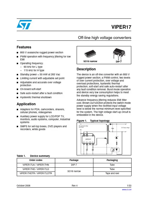
October 2008 Rev 41/33VIPER17Off-line high voltage convertersFeatures■800 V avalanche rugged power section ■PWM operation with frequency jittering for low EMI■Operating frequency: –60 kHz for L type –115 kHz for H type■Standby power < 50 mW at 265 Vac ■Limiting current with adjustable set point ■Adjustable and accurate over voltage protection■On-board soft-start■Safe auto-restart after a fault condition ■Hysteretic thermal shutdownApplication■Adapters for PDA, camcorders, shavers, cellular phones, videogames■Auxiliary power supply for LCD/PDP TV,monitors, audio systems, computer, industrial systems■SMPS for set-top boxes, DVD players and recorders, white goodsDescriptionThe device is an off-line converter with an 800 V rugged power section, a PWM control, two levels of over current protection, over voltage and overload protections, hysteretic thermalprotection, soft-start and safe auto-restart after any fault condition removal. Burst mode operation and device very low consumption helps to meet the standby energy saving regulations.Advance frequency jittering reduces EMI filter cost. Brown-out function protects the switch mode power supply when the rectified input voltage level is below the normal minimum level specified for the system. The high voltage start-up circuit is embedded in the device.VIPER17Table 1.Device summaryOrder codesPackage Packaging VIPER17LN / VIPER17HN DIP-7Tube VIPER17HD / VIPER17LD SO16 narrowTube VIPER17HDTR / VIPER17LDTRT ape and reelContents VIPER17Contents1Block diagram . . . . . . . . . . . . . . . . . . . . . . . . . . . . . . . . . . . . . . . . . . . . . . 4 2Typical power . . . . . . . . . . . . . . . . . . . . . . . . . . . . . . . . . . . . . . . . . . . . . . . 43Pin settings . . . . . . . . . . . . . . . . . . . . . . . . . . . . . . . . . . . . . . . . . . . . . . . . 53.1Connection diagram . . . . . . . . . . . . . . . . . . . . . . . . . . . . . . . . . . . . . . . . . . 53.2Pin description . . . . . . . . . . . . . . . . . . . . . . . . . . . . . . . . . . . . . . . . . . . . . . 54Electrical data . . . . . . . . . . . . . . . . . . . . . . . . . . . . . . . . . . . . . . . . . . . . . . 64.1Maximum ratings . . . . . . . . . . . . . . . . . . . . . . . . . . . . . . . . . . . . . . . . . . . . 64.2Thermal data . . . . . . . . . . . . . . . . . . . . . . . . . . . . . . . . . . . . . . . . . . . . . . . 64.3Electrical characteristics . . . . . . . . . . . . . . . . . . . . . . . . . . . . . . . . . . . . . . . 7 5Typical electrical characteristics . . . . . . . . . . . . . . . . . . . . . . . . . . . . . . 11 6Typical circuit . . . . . . . . . . . . . . . . . . . . . . . . . . . . . . . . . . . . . . . . . . . . . 147Operation descriptions . . . . . . . . . . . . . . . . . . . . . . . . . . . . . . . . . . . . . . 157.1Power section and gate driver . . . . . . . . . . . . . . . . . . . . . . . . . . . . . . . . . 157.2High voltage startup generator . . . . . . . . . . . . . . . . . . . . . . . . . . . . . . . . . 157.3Power-up and soft-start up . . . . . . . . . . . . . . . . . . . . . . . . . . . . . . . . . . . . 167.4Power down operation . . . . . . . . . . . . . . . . . . . . . . . . . . . . . . . . . . . . . . . 187.5Auto restart operation . . . . . . . . . . . . . . . . . . . . . . . . . . . . . . . . . . . . . . . . 187.6Oscillator . . . . . . . . . . . . . . . . . . . . . . . . . . . . . . . . . . . . . . . . . . . . . . . . . 187.7Current mode conversion with adjustable current limit set point . . . . . . . 197.8Over voltage protection (OVP) . . . . . . . . . . . . . . . . . . . . . . . . . . . . . . . . . 197.9About CONT pin . . . . . . . . . . . . . . . . . . . . . . . . . . . . . . . . . . . . . . . . . . . . 217.10Feed-back and over load protection (OLP) . . . . . . . . . . . . . . . . . . . . . . . 217.11Burst-mode operation at no load or very light load . . . . . . . . . . . . . . . . . . 247.12Brown-out protection . . . . . . . . . . . . . . . . . . . . . . . . . . . . . . . . . . . . . . . . 257.132nd level over current protection and hiccup mode . . . . . . . . . . . . . . . . . 27 2/33VIPER17Contents 8Package mechanical data . . . . . . . . . . . . . . . . . . . . . . . . . . . . . . . . . . . . 28 9Revision history . . . . . . . . . . . . . . . . . . . . . . . . . . . . . . . . . . . . . . . . . . . 323/33Block diagram VIPER174/331 Block diagram2 Typical powerTable 2.Typical powerPart number 230 V AC85-265 V ACAdapter (1)Open frame (2)Adapter (1)Open frame (2)VIPER179 W12 W5 W7 W1.Typical continuous power in non ventilated enclosed adapter measured at 50 °C ambient.2.Maximum practical continuous power in an open frame design at 50 °C ambient, with adequate heat sinking.VIPER17Pin settings5/333 Pin settings3.1 Connection diagram3.2 Pin descriptionTable 3.Pin descriptionPin N.NameFunctionDIP-7SO161 1...4GND This pin represents the device ground and the source of the power section. 25VDDSupply voltage of the control section. This pin also provides the charging currentof the external capacitor during start-up time.36CONTControl pin. The following functions can be selected:1. current limit set point adjustment. The internal set default value of the cycle-by-cycle current limit can be reduced by connecting to ground an external resistor.2. output voltage monitoring. A voltage exceeding 3 V shuts the IC downreducing the device consumption. This function is strobed and digitally filtered for high noise immunity.47FBControl input for duty cycle control. Internal current generator provides bias current for loop regulation. A voltage below 0.5 V activates the burst-mode operation. A level close to 3.3 V means that we are approaching the cycle-by-cycle over-current set point.510BRBrownout protection input with hysteresis. A voltage below 0.45 V shuts down (not latch) the device and lowers the power consumption. Device operation restarts as the voltage exceeds 0.45 V plus hysteresis voltage. It can be connected to ground when not used.7,813...16DRAINHigh voltage drain pin. The built-in high voltage switched start-up bias current is drawn from this pin too.Electrical data VIPER176/334 Electrical data4.1 Maximum ratings4.2 Thermal dataTable 4.Absolute maximum ratingsSymbol Pin(DIP7)ParameterValue Unit V DRAIN 7, 8Drain-to-source (ground) voltage800V E AV 7, 8Repetitive avalanche energy (limited by T J = 150 °C)2mJ I AR 7, 8Repetitive avalanche current (limited by T J = 150 °C)1A I DRAIN 7, 8Pulse drain current2.5A V CONT 3Control input pin voltage (with I CONT = 1 mA)Self limited V V FB 4Feed-back voltage -0.3 to 5.5V V BR 5Brown-out input pin voltage 2V V DD 2Supply voltage (I DD = 25 mA)Self limitedV I DD 2Input current25mA P TOT Power dissipation at T A < 50 °C 1W T J Operating junction temperature range -40 to 150°C T STGStorage temperature-55 to 150°CTable 5.Thermal dataSymbol ParameterMax value SO16N Max value DIP7Unit R thJP Thermal resistance junction pin 3540°C/W R thJAThermal resistance junction ambient (1)1.When mounted on a standard single side FR4 board with 100 μm 2 (0.155 sq in) of Cu (35 μm thick)8090°C/WVIPER17Electrical data7/334.3 Electrical characteristics(T J = -25 to 125 °C, V DD = 14 V; unless otherwise specified)Table 6.Power sectionSymbol ParameterTest condition Min TypMaxUnit V BVDSS Break-down voltage I DRAIN = 1 mA, V FB = GNDT J = 25 °C800V I OFFOFF state drain currentV DRAIN = max rating,V FB = GND60μA R DS(on)Drain-source on state resistanceI DRAIN = 0.2 A, V FB = 3 V , V BR = GND, T J = 25 °C 2024ΩI DRAIN = 0.2 A , V FB = 3 V , V BR = GND, T J = 125 °C 4048ΩC OSSEffective (energy related) output capacitanceV DRAIN = 0 to 640 V10pFTable 7.Supply sectionSymbol ParameterTest conditionMinTypMaxUnitVoltageV DRAIN _STARTDrain-source start voltage6080100V I DDchStart up charging currentV DRAIN = 120 V ,V BR = GND, V FB = GND, V DD = 4 V-2-3-4mAV DRAIN = 120 V ,V BR = GND, V FB = GND,V DD = 4 V after fault.-0.4-0.6-0.8mA V DD Operating voltage range After turn-on 8.523.5V V DDclamp V DD clamp voltage I DD = 20 mA23.5V V DDon V DD start up threshold V DRAIN = 120 V , V BR = GND, V FB = GND131415V V DDoffV DD under voltage shutdown threshold 7.588.5V V DD(REST ART)V DD restart voltage thresholdV DRAIN = 120 V ,V BR = GND, V FB = GND44.55VCurrentI DD0Operating supply current, not switchingV FB = G ND, F SW = 0 kHz, V BR = GND, V DD = 10 V 0.9mA I DD1Operating supply current, switchingV DRAIN = 120 V , F SW = 60 kHz1.8mA V DRAIN = 120 V ,F SW = 115 kHz2mA I DD_FAULT Operating supply current, with protection tripping 400μA I DD_OFFOperating supply current with V DD < VDD_offV DD = 7 V270μAElectrical data VIPER178/33Table 8.Controller section(T J = -25 to 125 °C, V DD = 14 V; unless otherwise specified) Symbol Parameter Test condition Min Typ Max Unit Feed-back pinV FBolpOver load shut downthreshold4.7 4.85.2VV FBlin Linear dynamics upper limit 3.2 3.3 3.4V V FBbm Burst mode threshold Voltage falling0.40.50.6V V FBbmhys Burst mode hysteresis Voltage rising 50mVI FB Feed-back sourced currentV FB = 0.3 V-150-200-280uA3.3 V < V FB <4.8 V-3uAR FB(DYN)Dynamic resistance V FB < 3.3 V1419kΩH FBΔV FB / ΔI D49V/A CONT pinVCONT_l Low level clamp voltage I CONT = -100 μA0.5V Current limitationI Dlim Max drain current limitationV FB = 4 V,I CONT = -10 µAT J = 25 °C0.380.40.42At SS Soft-start time8.5ms T ON_MIN Minimum turn ON time 220400480ns td Propagation delay 100ns t LEB Leading edge blanking 300nsI D_BMPeak drain current duringburst modeV FB = 0.6 V90mA Oscillator sectionF OSCVIPER17L V DD = operatingvoltage range,V FB = 1 V546066kHz VIPER17H103115127kHz FD Modulation depthVIPER17L±4kHzVIPER17H ±8kHz FM Modulation frequency250HzD MAX Maximum duty cycle 7080%VIPER17Electrical data9/33Table 8.Controller section (continued)(T J = -25 to 125 °C, V DD = 14 V; unless otherwise specified)SymbolParameterTest conditionMinTypMaxUnitOver current protection (2nd OCP)I DMAXSecond over current threshold0.6AOver voltage protectionV OVP Over voltage protection threshold2.73 3.3V T STROBEOver voltage protection strobe time2.2μsBrown out protectionV BRth Brown out threshold Voltage falling0.410.450.49V V BRhyst Voltage hysteresis above V BRth50mV I BRhyst Current hysteresis 710μA V BR Operating range0.152V V DISBrown out disable voltage50150mVThermal shutdownT SD Thermal shutdown temperature 150170°C T HYSTThermal shutdown hysteresis30°CElectrical data VIPER1710/33Figure 4.Minimum turn-on time test circuitFigure 5.Brown out threshold test circuitsFigure 6.OVP threshold test circuits(The OVP protection is triggeredafter four consecutive oscillator cycles)11/335 Typical electrical characteristicsFigure 7.Current limit vs T JFigure 8.Switching frequency vs T JFigure 9.Drain start voltage vs T J Figure 10.HFB vs T JFigure 11.Brown out threshold vs T JFigure 12.Brown out hysteresis vs T J12/33Figure 13.Brown out hysteresis currentvs T JFigure 14.Operating supply current(no switching) vs TJFigure 15.Operating supply current(switching) vs TJFigure 16.current limit vs RLIMFigure 17.Power MOSFET on-resistancevs T JFigure 18.Power MOSFET break downvoltage vs T J13/33Typical circuit VIPER1714/336 Typical circuitVIPER17Operation descriptions15/337 Operation descriptionsVIPER17 is a high-performance low-voltage PWM controller chip with an 800 V, avalancherugged Power section.The controller includes: the oscillator with jittering feature, the start up circuits with soft-start feature, the PWM logic, the current limit circuit with adjustable set point, the second over current circuit, the burst mode management, the brown-out circuit, the UVLO circuit, the auto-restart circuit and the thermal protection circuit.The current limit set-point is set by the CONT pin. The burst mode operation guaranties high performance in the stand-by mode and helps in the energy saving norm accomplishment.All the fault protections are built in auto restart mode with very low repetition rate to prevent IC's over heating.7.1 Power section and gate driverThe power section is implemented with an avalanche ruggedness N-channel MOSFET, which guarantees safe operation within the specified energy rating as well as high dv/dt capability. The Power section has a BV DSS of 800 V min. and a typical R DS(on) of 20 Ω at 25 °C.The integrated SenseFET structure allows a virtually loss-less current sensing.The gate driver is designed to supply a controlled gate current during both turn-on and turn-off in order to minimize common mode EMI. Under UVLO conditions an internal pull-down circuit holds the gate low in order to ensure that the Power section cannot be turned on accidentally.7.2 High voltage startup generatorThe HV current generator is supplied through the DRAIN pin and it is enabled only if the input bulk capacitor voltage is higher than V DRAIN_ST ART threshold, 80 V DC typically. When the HV current generator is ON, the IDD_ch current (3 mA typical value) is delivered to the capacitor on the V DD pin. In case of Auto Restart mode after a fault event, the IDD_chcurrent is reduced to 0.6 mA, typ. in order to have a slow duty cycle during the restart phase.Operation descriptions VIPER1716/337.3 Power-up and soft-start upIf the input voltage rises up till the device start level (V DRAIN_ST ART ), the V DD voltage begins to grow due to the IDD_ch current (see Table 7 on page 7) coming from the internal high voltage start up circuit. If the V DD voltage reaches V DDon threshold (~14 V) the power MOSFET starts switching and the HV current generator is turned OFF . See Figure 23 on page 17.The IC is powered by the energy stored in the capacitor on the VDD pin, C VDD , until when the self-supply circuit (typically an auxiliary winding of the transformer and a steering diode) develops a voltage high enough to sustain the operation.C VDD capacitor must be sized enough to avoid fast discharge and keep the needed voltage value higher than V DDoff threshold. In fact, a too low capacitance value could terminate the switching operation before the controller receives any energy from the auxiliary winding. The following formula can be used for the V DD capacitor calculation:Equation 1The t SSaux is the time needed for the steady state of the auxiliary voltage. This time is estimated by applicator according to the output stage configurations (transformer, output capacitances, etc.).During the converter start up time, the drain current limitation is progressively increased to the maximum value. In this way the stress on the secondary diode is considerably reduced. It also helps to prevent transformer saturation. The soft-start time lasts 8.5 ms and the feature is implemented for every attempt of start up converter or after a fault.C VDD I DDch t SSaux ×V DDon V DDoff–----------------------------------------=VIPER17Operation descriptions17/33Operation descriptions VIPER177.4 Power down operationAt converter power down, the system loses regulation as soon as the input voltage is so lowthat the peak current limitation is reached. The V DD voltage drops and when it falls belowthe V DDoff threshold (8 V typical) the power MOSFET is switched OFF, the energy transfersto the IC interrupted and consequently the V DD voltages decreases, Figure23 on page17.Later, if the V IN is lower than V DRAIN_START (80 V typical), the start up sequence is inhibitedand the power down completed. This feature is useful to prevent converter’s restart attemptsand ensures monotonic output voltage decay during the system power down.7.5 Auto restart operationIf after a converter power down, the V IN is higher than V DRAIN_ST ART, the start up sequenceis not inhibited and will be activated only when the V DD voltage drops down the V DDrestartthreshold (4.5 V typical). This means that the HV start up current generator restarts the V DDcapacitor charging only when the V DD voltage drops below V DDrestart. The scenario abovedescribed is for instance a power down because of a fault condition. After a fault condition,the charging current is 0.6 mA (typ.) instead of the 3 mA (typ.) of a normal start up converterphase. This feature together with the low V DDrestart threshold (4.5 V) ensures that, after afault, the restart attempts of the IC has a very long repetition rate and the converter workssafely with extremely low power throughput. The Figure25 shows the IC behavioral after ashort circuit event.7.6 OscillatorThe switching frequency is internally fixed to 60 kHz or 115 kHz. In both case the switchingfrequency is modulated by approximately ±4 kHz (60 kHz version) or ±8 kHz(115 kHz version) at 250 Hz (typical) rate, so that the resulting spread-spectrum actiondistributes the energy of each harmonic of the switching frequency over a number of side-band harmonics having the same energy on the whole but smaller amplitudes.18/33VIPER17Operation descriptions19/337.7Current mode conversion with adjustable current limit set pointThe device is a current mode converter: the drain current is sensed and converted in voltage that is applied to the non inverting pin of the PWM comparator. This voltage is compared with the one on the feed-back pin through a voltage divider on cycle by cycle basis.The VIPER17 has a default current limit value, I DLIM , that the designer can adjust according the electrical specification, by the R LIM resistor connected to the CONT see Figure 16 on page 12.The CONT pin has a minimum current sunk needed to activate the I DLIM adjustment: without R LIM or with high R LIM (i.e. 100 K Ω) the current limit is fixed to the default value (see I DLIM , Table 8 on page 8).7.8 Over voltage protection (OVP)The device can monitor the converter output voltage. This operation is done by CONT pin during power MOSFET OFF-time, when the voltage generated by the auxiliary winding tracks converter's output voltage, through turn ratio See Figure 26.In order to perform the output voltage monitor, the CONT pin has to be connected to the aux winding through a resistor divider made up by R LIM and R OVP (see Figure 21 and Figure 27). If the voltage applied to the CONT pin exceeds the internal 3 V reference for fourconsecutive times the controller recognizes an over voltage condition. This special feature uses an internal counter; that is to reduce sensitivity to noise and prevent the latch from being erroneously activated. see Figure 26 on page 20. The counter is reset every time the OVP signal is not triggered in one oscillator cycle.Referring to the Figure 21, the resistors divider ratio k OVP will be given by:Equation 2Equation 3N AUXN SEC--------------k OVP V OVPN AUXN SEC--------------V OUTOVP V DSEC +()V DAUX –⋅--------------------------------------------------------------------------------------------------=k OVP R LIMR LIM R OVP+---------------------------------=Operation descriptions VIPER1720/33Where:●V OVP is the OVP threshold (see Table8 on page9)●V OUT OVP is the converter output voltage value to activate the OVP (set by designer)designer●N AUX is the auxiliary winding turns●N SEC is the secondary winding turns●V DSEC is the secondary diode forward voltage●V DAUX is the auxiliary diode forward voltage●R OVP together R LIM make the output voltage dividerThan, fixed R LIM, according to the desired I DLIM, the R OVP can be calculating by: Equation 4The resistor values will be such that the current sourced and sunk by the CONT pin be within the rated capability of the internal clamp.R OVP R LIM1k OVP–k OVP----------------------×=VIPER17Operation descriptions21/337.9 About CONT pinReferring to the Figure 27, through the CONT PIN, the below features can be implemented:1.Current Limit set point2.Over voltage protection on the converter output voltageThe Table 9on page 21 referring to the Figure 27, lists the external resistance combinations needed to activate one or plus of the CONT pin functions.7.10 Feed-back and over load protection (OLP)The VIPER17 is a current mode converter: the feedback pin controls the PWM operation, controls the burst mode and actives the overload protection of the device. Figure 28 on page 23 and Figure 29 show the internal current mode structure.With the feedback pin voltage between V FBbm and V FBlin , (respectively 0.5 V and 3.3 V ,typical values) the drain current is sensed and converted in voltage that is applied to the non inverting pin of the PWM comparator.This voltage is compared with the one on the feedback pin through a voltage divider on cycle by cycle basis. When these two voltages are equal, the PWM logic orders the switch off of the power MOSFET . The drain current is always limited to I DLIM value.In case of overload the feedback pin increases in reaction to this event and when it goes higher than V FBlin the drain current is limited or to the default I DLIM value or the one imposedTable 9.CONT pin configurationsFunction / componentR LIM (1)1.R LIM have to be fixed before R FF and R OVPR OVP D AUX I Dlim reductionSee Figure 8No No OVP≥ 80 K ΩSee Equation 4Y es I Dlim reduction + OVPSee Figure 8See Equation 4Y esOperation descriptions VIPER1722/33through a resistor at the CONT pin (using the R LIM, see Figure16 on page12); the PWM comparator is disabled.At the same time an internal current generator starts to charge the feedback capacitor (C FB) and when the feedback voltage reaches the V FBolp threshold, the converter is turned off and the start up phase is activated with reduced value of I charge to 0.6 mA.During the first start up phase of the converter, after the soft-start up time (typical value is 8.5 ms) the output voltage could force the feedback pin voltage to rise up to the V FBolp threshold that switches off the converter itself.To avoid this event, the appropriate feedback network has to be selected according to the output load. More the network feedback fixes the compensation loop stability. The Figure28 on page23 and Figure29 show the two different feedback networks.The time from the over load detection (VFB = V FBlin) to the device shutdown(VFB = V FBolp) can be calculating by C FB value (see Figure28 on page23 and Figure29), using the formula:Equation 5In the Figure28, the capacitor connected to FB pin (C FB) is used as part of the circuit to compensate the feedback loop but also as element to delay the OLP shut down owing to the time needed to charge the capacitor (see equation 5).After the start up time, 8.5 ms typ value, during which the feedback voltage is fixed at V FBlin, the output capacitor could not be at its nominal value and the controller interpreter this situation as an over load condition. In this case, the OLP delay helps to avoid an incorrect device shut down during the start up.Owing to the above considerations, the OLP delay time must be long enough to by-pass the initial output voltage transient and check the over load condition only when the output voltage is in steady state. The output transient time depends from the value of the output capacitor and from the load.When the value of the C FB capacitor calculated for the loop stability is too low and cannot ensure enough OLP delay, an alternative compensation network can be used and it is showed in Figure29 on page23.Using this alternative compensation network, two poles (f PFB, f PFB1) and one zero (f ZFB) are introduced by the capacitors C FB and C FB1 and the resistor R FB1.The capacitor C FB introduces a pole (f PFB) at higher frequency than f ZB and f PFB1. This pole is usually used to compensate the high frequency zero due to the ESR (Equivalent Series Resistor) of the output capacitance of the fly-back converter.The mathematical expressions of these poles and zero frequency, considering the scheme in Figure29 are reported by the equations below:Equation 6T OLP delay–C FBV FBolp V FBlin–3μA---------------------------------------×=VIPER17Operation descriptions Equation 7Equation 8The R FB(DYN) is the dynamic resistance seen by the FB pin.The C FB1 capacitor fixes the OLP delay and usually C FB1 results much higher than C FB.The Equation 5 can be still used to calculate the OLP delay time but C FB1 has to beconsidered instead of C FB. Using the alternative compensation network, the designer cansatisfy, in all case, the loop stability and the enough OLP delay time alike.23/33Operation descriptions VIPER177.11 Burst-mode operation at no load or very light loadWhen the voltage on feedback pin falls down 50 mV below the burst mode threshold, V FBbm,power MOSFET is not more allowed to be switched on. It can be switched on again if thevoltage on feedback pin exceeds V FBbm. The voltage on PWM comparator non invertinginternal input, connected to feedback pin through a resistive voltage divider, is lowerclamped to a certain value leading to a minimum value, of 90 mA (typ.) for the drain peakcurrent.When the load decrease the feedback loop reacts lowering the feedback pin voltage. As thevoltage goes 50 mV below V FBbm MOSFET stops switching. After the MOSFET stops, as aresult of the feedback reaction to the energy delivery stop, the feedback pin voltageincreases and exceeding V FBbm threshold MOSFET the power device start switching again.Figure30 shows this behavior called burst mode. Systems alternates period of time wherepower MOSFET is switching to period of time where power MOSFET is not switching. Thepower delivered to output during switching periods exceeds the load power demands; theexcess of power is balanced from not switching period where no power is processed. Theadvantage of burst mode operation is an average switching frequency much lower then thenormal operation working frequency, up to some hundred of hertz, minimizing all frequencyrelated losses.24/33VIPER17Operation descriptions25/337.12 Brown-out protectionBrown-out protection is a not-latched shutdown function activated when a condition of mainsunder voltage is detected.The Brown-out comparator is internally referenced to V BRth ,0.45 V typ value, and disables the PWM if the voltage applied at the BR pin is below this internal reference. Under this condition the power MOSFET is turned off. Until the Brown out condition is present, the VDD voltage continuously oscillates between the V DDon and the UVLO thresholds, as shown in the timing diagram of Figure 31 on page 25. A voltage hysteresis is present to improve the noise immunity.The switching operation is restarted as the voltage on the pin is above the reference plus the before said voltage hysteresis. See Figure 31.The Brown-out comparator is provided also with a current hysteresis, I BRhyst .With thisapproach is possible to set the V INon threshold and V INoff thresholds separately, by properly choosing the resistors of the divider connect to the BR pin.Fixed the V INon and the V INoff levels, with reference to Figure 31, the following relationships can be established for the calculation of the resistors R H and R L :Equation 9。
本文部分内容来自网络整理,本司不为其真实性负责,如有异议或侵权请及时联系,本司将立即删除!== 本文为word格式,下载后可方便编辑和修改! ==word实验指导书篇一:word实验指导书第3章文字处理软件Word3.1 Word 201X概述实验3-1 Word的启动、退出和界面介绍1. 实验目的① 掌握Word应用程序快捷方式的建立。
② 通过快捷方式掌握Word的启动和退出。
③ 熟悉Word的工作界面和视图显示方式。
2. 实验内容建立Word的快捷方式,并利用该快捷方式启动Word,观察word用户界面,并把文档窗口的显示方式设为普通视图。
3. 实验步骤① 执行“开始”|“搜索”|“文件或文件夹”命令,打开“搜索结果”窗口,搜索的Word应用程序文件名为“Winword.exe”。
② 在搜索结果中选定Word应用程序文件,在桌面为其创建快捷方式。
③ 双击“Word快捷方式”图标,打开Word应用程序,认识Word工作界面:标题栏、菜单栏、工具栏、状态栏、文档窗口和任务窗格等,如图3-1所示。
④ 单击“普通视图”切换按钮或执行“视图”|“普通”命令,把视图模式切换为普通视图,接着采用同样的方法把视图方式切换为页面视图。
比较两种视图方式的区别。
⑤ 单击标题栏上的“关闭”按钮或执行“文件”|“关闭”命令,退出Word应用程序。
【小技巧】普通视图和页面视图的区别:普通视图是Word最基本的视图方式,其显示速度相对较快,非常适合于文字的录入阶段。
用户可在该视图方式下进行文字的录入及编辑工作。
在普通视图下不显示页边距、页眉和页脚、背景、图形对象。
页面视图方式即直接按照用户设置的页面大小显示,此时的显示效果与打印效果一致,用户可从中看到各种对象(包括页眉、页脚、水印和图形等),这对于编辑页眉和页脚,调整页边距,以及处理边框、图形对象及分栏都是很有用的。
菜单栏工具栏文档窗口标题栏 Word程序关闭按钮文档窗口关闭按钮水平标尺垂直滚动条任务窗格视图切换按钮文档编辑区垂直标尺水平滚动条状态栏图3-1 Word的工作窗口实验3-2 Word工具栏定制和系统设置1. 实验目的① 掌握工具栏的定制。


通过正确的 PCB 布局优化 SAR ADC 性能作者:Matthias TaenzerTI 公司16 位或更高精度的 ADC 依靠一款精心的电路板设计来获得电源品质测量、多轴马达控制或纯工业数据采集应用的理想性能。
除清洁的输入信号外,参考信号和电源电压也会严重破坏转换结果。
正确的去耦、接地和信号调节有助于提高系统性能。
由于 6 通道 ADS8556 具有复杂性、内部参考及高压输入,因此可以将其作为一个较好的例子。
下列步骤将介绍避免非必要线性误差所需的各种方法,同时还将说明错误布局引起失真的一些情形。
第一步:优化参考路径在高性能 ADC 应用中,参考输入是最为关键的信号路径。
其必须在 1/2 转换时钟周期内达到 16 位精度。
另外,该终端的噪声、失真和偏移量都会直接影响转换结果的质量。
ADS8556 具有一个内部参考源,其可向三个路径对中的每一个路径提供缓冲参考电压。
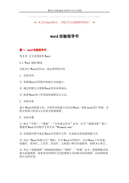
RefIO RefGNDC C图 1 ADS8556 的简化结构图作为备选方案,内部参考模块在失效时,可外部施加参考电压。
在这两种情况下都需要使用一个外部去耦电容 ,以在后续转换步骤期间为内部电容阵列再充电提供电荷。
因此, 的大小由内部负载电容的大小决定。
假设一个转换周期 期间的压降必须小于 ,则可使用 计算外部去耦电容。
表示内部 CDAC 总电容, 为位数。
refext C refext C conv t LSB 5.0tot n refext C C ⋅≥+)1(2tot C n要对压降进行补偿,参考缓冲器(内部或外部)需使用规定精度(例如:LSB/4 或 LSB/8)为去耦电容再充电至 提供电流。
基于这些考虑因素,参考缓冲器必须满足下列带宽要求(假设 ref V τ1 稳定):convdB t f ⋅=−π2)2ln(3.如果实施一个外部缓冲器来驱动参考电压,则不仅仅要考虑去耦电容,还应考虑到缓冲器输出到电容以及 ADC 参考输入的电阻。