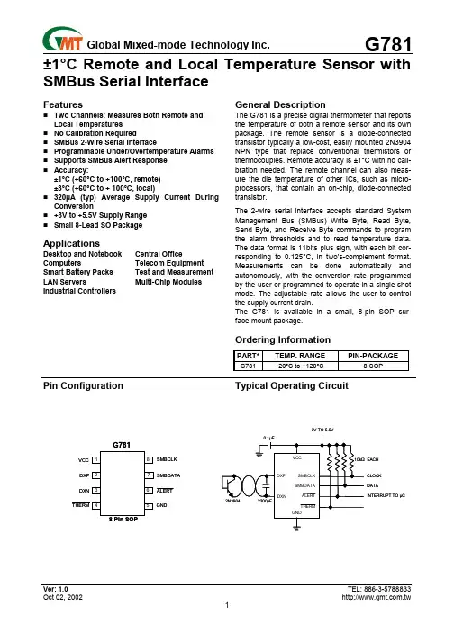
±1°C Remote and Local Temperature Sensor with SMBus Serial InterfaceFeaturesTwo Channels: Measures Both Remote andLocal Temperatures No Calibration RequiredSMBus 2-Wire Serial InterfaceProgrammable Under/Overtemperature Alarms Supports SMBus Alert Response Accuracy:±1°C (+60°C to +100°C, remote) ±3°C (+60°C to + 100°C, local)320µA (typ) Average Supply Current During Conversion+3V to +5.5V Supply Range Small 8-Lead SO PackageApplications Desktop and Notebook Central Office Computers Telecom Equipment Smart Battery Packs Test and Measurement LAN Servers Multi-Chip Modules Industrial Controllers General DescriptionThe G781 is a precise digital thermometer that reports the temperature of both a remote sensor and its own package. The remote sensor is a diode-connected transistor typically a low-cost, easily mounted 2N3904 NPN type that replace conventional thermistors or thermocouples. Remote accuracy is ±1°C with no cali-bration needed. The remote channel can also meas-ure the die temperature of other ICs, such as micro-processors, that contain an on-chip, diode-connected transistor.The 2-wire serial interface accepts standard System Management Bus (SMBus) Write Byte, Read Byte, Send Byte, and Receive Byte commands to program the alarm thresholds and to read temperature data.The data format is 11bits plus sign, with each bit cor-responding to 0.125°C, in two’s-complement format. Measurements can be done automatically and autonomously, with the conversion rate programmed by the user or programmed to operate in a single-shot mode. The adjustable rate allows the user to control the supply current drain.The G781 is available in a small, 8-pin SOP sur-face-mount package.Ordering InformationPART* TEMP. RANGE PIN-PACKAGEG781-20°C to +120°C8-SOPPin ConfigurationTypical Operating Circuit3V TO 5.5VEACHCLOCK DATAINTERRUPT TO µCSMBDATA SMBCLK GNDG781ALERTAbsolute Maximum RatingsVCC to GND………….….……..………….-0.3V to +6V DXP to GND……….……………..…-0.3V to VCC + 0.3V DXN to GND……………..……………..-0.3V to +0.8V SMBCLK, SMBDATA,ALERT to GND..…-0.3V to +6V SMBDATA,ALERT Current………….-1mA to +50mA DXN Current……………………..………………….±1mA ESD Protection (SMBCLK, SMBDATA,ALERT , humanbody model).……………………………………….2000V ESD Protection (other pins, human body model)..2000V Continuous Power Dissipation (T A = +70°C) ..SOP (derate 8.30mW/°C above +70°C)…………......667mW Operating Temperature Range………-20°C to +120°C Junction Temperature………………….………..+150°C Storage temperature Range………….-65°C to +165°C Lead Temperature (soldering, 10sec)……..……...+300°CStresses beyond those listed under “Absolute Maximum Ratings” may cause permanent damage to the device. These are stress ratings only, and functional operation of the device at these or any other conditions beyond those indicated in the opera-tional sections of the specifications is not implied. Exposure to absolute maximum rating conditions for extended periods may affect device reliability.Electrical Characteristics(VCC = + 3.3V, T A = 0°C to +85°C, unless otherwise noted.)PARAMETER CONDITIONS MIN TYP MAX UNITST R = +60°C to +100°C, VCC = 3.0V to 3.6V-1+1Temperature Error, Remote Di-ode (Note 1)T R = 0°C to +125°C (Note 2)-3 +3 °CT A = +60°C to +100°C-3 +3Temperature Error, Local DiodeT A = 0°C to +85°C (Note 2)-5 +5°CSupply-Voltage Range3.0 5.5 V Undervoltage Lockout Threshold VCC input, disables A/D conversion, rising edge 2.8 V Undervoltage Lockout Hysteresis 50 mV Power-On Reset Threshold VCC, falling edge 1.7 V POR Threshold Hysteresis 50 mVSMBus static3Standby Supply Current Logic inputs forced to VCC or GND Hardware or softwarestandby, SMBCLK at 10kHz4 µA0.5 conv/sec 35Average Operating Supply CurrentAuto-convert mode. Logic inputs forced to VCC or GND 8.0 conv/sec 320 µAConversion Time From stop bit to conversion complete (both channels) 125 ms Conversion Rate Timing Conversion-Rate Control Byte=04h, 1Hz 1 sec High level176Remote-Diode Source CurrentDXP forced to 1.5VLow level11µAElectrical Characteristics (continued)(VCC = + 3.3V, T A = 0 to +85°C, unless otherwise noted.)Note 1: A remote diode is any diode-connected transistor from Table1. T R is the junction temperature of the remote of the remote diode. See Remote Diode Selection for remote diode forward voltage requirements.Note 2: Guaranteed by design but not 100% tested.Pin DescriptionDetailed DescriptionThe G781 is a temperature sensor designed to work in conjunction with an external microcontroller (µC) or other intelligence in thermostatic, process-control, or monitoring applications. The µC is typically a power- management or keyboard controller, generating SMBus serial commands by “bit-banging” general- purpose input-output (GPIO) pins or via a dedicated SMBus interface block.Essentially an serial analog-to digital converter (ADC) with a sophisticated front end, the G781 contains a switched current source, a multiplexer, an ADC, an SMBus interface, and associated control logic (Figure 1). Temperature data from the ADC is loaded into two data registers, where it is automatically compared with data previously stored in several over/under- tem-perature alarm registers.ADC and MultiplexerThe ADC is an averaging type that integrates over a 60ms period (each channel, typical), with excellent noise rejection.The multiplexer automatically steers bias currents through the remote and local diodes, measures their forward voltages, and computes their temperatures. Both channels are automatically converted once the conversion process has started, either in free-running or single-shot mode. If one of the two channels is not used, the device still performs both measurements, and the user can simply ignore the results of the un-used channel. If the remote diode channel is unused, tie DXP to DXN rather than leaving the pins open. The worst-case DXP-DXN differential input voltage range is 0.25V to 0.95V.Excess resistance in series with the remote diode causes about +0.6°C error per ohm. Likewise, 240µV of offset voltage forced on DXP-DXN causes about 1°C error.Figure 1. Functional DiagramSMBDATA SMBCLKA/D Conversion SequenceIf a Start command is written (or generated automati-cally in the free-running auto-convert mode), both channels are converted, and the results of both meas-urements are available after the end of conversion. A BUSY status bit in the status byte shows that the de-vice is actually performing a new conversion; however, even if the ADC is busy, the results of the previous conversion are always available.Remote Diode SelectionTemperature accuracy depends on having a good- quality, diode-connected small-signal transistor. The G781 can also directly measure the die temperature of CPUs and other integrated circuits having on-board temperature-sensing diodes.The transistor must be a small-signal type with a rela-tively high forward voltage; otherwise, the A/D input voltage range can be violated. The forward voltage must be greater than 0.25V at 10µA; check to ensure this is true at the highest expected temperature. The forward voltage must be less than 0.95V at 300µA; check to ensure this is true at the lowest expected temperature. Large power transistors don’t work at all. Also, ensure that the base resistance is less than 100Ω. Tight specifications for forward-current gain (+50 to +150, for example) indicate that the manufac-turer has good process controls and that the devices have consistent V be characteristics.Thermal Mass and Self-HeatingThermal mass can seriously degrade the G781’s ef-fective accuracy. The thermal time constant of the SOP- package is about 140 in still air. For the G781 junction temperature to settle to within +1°C after a sudden +100°C change requires about five time con-stants or 12 minutes. The use of smaller packages for remote sensors, such as SOT23s, improves the situa-tion. Take care to account for thermal gradients be-tween the heat source and the sensor, and ensure that stray air currents across the sensor package do not interfere with measurement accuracy. Self-heating does not significantly affect measurement accuracy. Remote-sensor self-heating due to the diode current source is negligible. For the local diode, the worst-case error occurs when auto-converting at the fastest rate and simultaneously sinking maximum current at the ALERT output. For example, at an 8Hz rate and with ALERT sinking 1mA, the typical power dissipation isVCC x 320µA plus 0.4V x 1mA. Package theta J-A is about 120°C /W, so with VCC = 3.3V and no copper PC board heat-sinking, the resulting temperature rise is:dT =1.45mW x 120°C /W =0.17°CEven with these contrived circumstances, it is difficultto introduce significant self-heating errors.Table 1. Remote-Sensor Transistor Manufacturers MANUFACTURER MODELNUMBER Philips PMBS3904Motorola(USA) MMBT3904 National Semiconductor (USA) MMBT3904Note:Transistors must be diode-connected (baseshorted to collector).ADC Noise FilteringThe ADC is an integrating type with inherently good noise rejection. Micropower operation places con-straints on high-frequency noise rejection; therefore, careful PC board layout and proper external noise fil-tering are required for high-accuracy remote meas-urements in electrically noisy environments.High-frequency EMI is best filtered at DXP and DXNwith an external 2200pF capacitor. This value can be increased to about 3300pF(max), including cable ca-pacitance. Higher capacitance than 3300pF introduces errors due to the rise time of the switched current source.Nearly all noise sources tested cause the ADC meas-urements to be higher than the actual temperature, typically by +1°C to 10°C, depending on the frequencyand amplitude.PC Board LayoutPlace the G781 as close as practical to the remote diode. In a noisy environment, such as a computer motherboard, this distance can be 4 in. to 8 in. (typical)or more as long as the worst noise sources (such as CRTs, clock generators, memory buses, and ISA/PCI buses) are avoided.Do not route the DXP-DXN lines next to the deflection coils of a CRT. Also, do not route the traces across a fast memory bus, which can easily introduce +30°C error, even with good filtering, Otherwise, most noise sources are fairly benign.Route the DXP and DXN traces in parallel and in close proximity to each other, away from any high-voltage traces such as +12V DC. Leakage currents from PC board contamination must be dealt with carefully, since a 10MΩ leakage path from DXP to ground causes about +1°C error.Connect guard traces to GND on either side of the DXP-DXN traces (Figure 2). With guard traces in place, routing near high-voltage traces is no longer an issue.Route through as few vias and crossunders as possible to minimize copper/solder thermocouple ef-fects.When introducing a thermocouple, make sure that both the DXP and the DXN paths have matching thermocouples. In general, PC board-induced ther-mocouples are not a serious problem, A copper-solder thermocouple exhibits 3µV/°C, and it takes about 240µV of voltage error at DXP-DXN to cause a +1°C measurement error. So, most parasitic thermocouple errors are swamped out.Use wide traces. Narrow ones are more inductive and tend to pick up radiated noise. The 10 mil widths and spacing recommended on Figure 2 aren’t absolutely necessary (as they offer only a minor improvement in leakage and noise), but try to use them where practi-cal.Keep in mind that copper can’t be used as an EMI shield, and only ferrous materials such as steel work will. Placing a copper ground plane between the DXP-DXN traces and traces carrying high-frequency noise signals does not help reduce EMI.PC Board Layout ChecklistPlace the G781 close to a remote diode.Keep traces away from high voltages (+12V bus).Keep traces away from fast data buses and CRTs. Use recommended trace widths and spacing.Place a ground plane under the tracesUse guard traces flanking DXP and DXN and con necting to GND.Place the noise filter and the 0.1µF VCC bypass capacitors close to the G781.Figure 2. Recommended DXP/DXN PC Traces Twisted Pair and Shielded CablesFor remote-sensor distances longer than 8 in., or in particularly noisy environments, a twisted pair is rec-ommended. Its practical length is 6 feet to 12feet (typi cal) before noise becomes a problem, as tested in a noisy electronics laboratory. For longer distances, the best solution is a shielded twisted pair like that used for audio microphones. Connect the twisted pair to DXP and DXN and the shield to GND, and leave the shield’s remote end unterminated.Excess capacitance at DX_limits practical remote sen-sor distances (see Typical Operating Characteristics), For very long cable runs, the cable’s parasitic capaci-tance often provides noise filtering, so the 2200pF ca-pacitor can often be removed or reduced in value. Ca-ble resistance also affects remote-sensor accuracy; 1Ωseries resistance introduces about + 0.6°C error.Low-Power Standby ModeStandby mode disables the ADC and reduces the supply-current drain to about 10µA. Enter standby mode by forcing high to the RUN/STOP bit in the con-figuration byte register. Software standby mode be-haves such that all data is retained in memory, and the SMB interface is alive and listening for reads and writes.Software standby mode is not a shutdown mode. With activity on the SMBus, extra supply current is drawn (see Typical Operating Characteristics). In software standby mode, the G781 can be forced to perform A/D conversions via the one-shot command, despite the RUN/STOP bit being high.10 MILSMINIMUM10 MILS10 MILSIf software standby command is received while a con-version is in progress, the conversion cycle is trun-cated, and the data from that conversion is not latched into either temperature reading register. The previous data is not changed and remains available.Supply-current drain during the 125ms conversion period is always about 320µA. Slowing down the con-version rate reduces the average supply current (see Typical Operating Characteristics). In between con-versions, the instantaneous supply current is about 25µA due to the current consumed by the conversion rate timer. In standby mode, supply current drops to about 3µA. At very low supply voltages (under the power-on-reset threshold), the supply current is higher due to the address pin bias currents. It can be as high as 100µA, depending on ADD0 and ADD1 settings. SMBus Digital InterfaceFrom a software perspective, the G781 appears as a set of byte-wide registers that contain temperature data, alarm threshold values, or control bits, A stan-dard SMBus 2-wire serial interface is used to read temperature data and write control bits and alarm threshold data.Each A/D channel within the device responds to the same SMBus slave address for normal reads and writes.The G781 employs four standard SMBus protocols: Write Byte, Read Byte, Send Byte, and Receive Byte (Figure 3). The shorter Receive Byte protocol allows quicker transfers, provided that the correct data regis-ter was previously selected by a Read Byte instruction. Use caution with the shorter protocols in multi-master systems, since a second master could overwrite the command byte without informing the first master.The temperature data format is 11bits plus sign in twos-complement form for remote channel, with each data bit representing 0.125°C (Table 2,Table 3), transmitted MSB first. Table 2. Temperature Data Format(Two’s-Complement)DIGITAL OUTPUTDATA BITSTEMP.(°C)SIGN MSB LSB EXT+127.875 0 111 1111 111+126.375 0 111 1110 011+25.5 0 001 1001 100+1.75 0 000 0001 110+0.5 0 000 0000 100+0.125 0 000 0000 001-0.125 1 111 1111 111-1.125 1 111 1110 111-25.5 1 110 0110 100-55.25 1 100 1000 110-65.000 1 011 1111 000Table 3. Extended Temperature Data FormatEXTENDEDRESOLUTIONDATA BITS0.000°C 000000000.125°C 001000000.250°C 010000000.375°C 011000000.500°C 100000000.625°C 101000000.750°C 110000000.875°C 11100000Slave AddressThe G781 appears to the SMBus as one device hav-ing a common address for both ADC channels. The G781 device address is set to 1001100.The G781 also responds to the SMBus Alert Re-sponse slave address (see the Alert Response Ad-dress section).One-Shot RegisterThe One-shot register is to initiate a single conversion and comparison cycle when the device is in standby mode and auto conversion mode. The write operation to this register causes one-shot conversion and the data written to it is irrelevant and is not stored.Serial Bus Interface ReinitializationWhen SMBCLK are held low for more than 30ms (typical) during an SMBus communication the G781 will reinitiateits bus interface and be ready for a new transmission. Alarm Threshold RegistersFour registers store alarm threshold data, with high-temperature (T HIGH) and low-temperature (T LOW) registers for each A/D channel. If either measured temperature equals or exceeds the corresponding alarm threshold value, an ALERT interrupt is as-serted.The power-on-reset (POR) state of both T HIGH registers is full scale (01010101, or +85°C). The POR state of both T LOW registers is 0°C.Diode Fault AlarmThere is a fault detector at DXP that detects whether the remote diode has an open-circuit condition. At the beginning of each conversion, the diode fault is checked, and the status byte is updated. This fault de-tector is a simple voltage detector. If DXP rises above VCC – 1V (typical) due to the diode current source, a fault is detected and the device alarms through pulling ALERT low while the remote temperature reading doesn’t update in this condition. Note that the diode fault isn’t checked until a conversion is initiated, so im-mediately after power-on reset the status byte indicates no fault is present, even if the diode path is broken.If the remote channel is shorted (DXP to DXN or DXP to GND), the ADC reads 1000 0000(-128°C) so as not to trip either the T HIGH or T LOW alarms at their POR settings. ALERT InterruptsThe ALERT interrupt output signal is latched and canonly be cleared by reading the Alert Response ad-dress. Interrupts are generated in response to T HIGHand T LOW comparisons and when the remote diode is disconnected (for fault detection). The interrupt doesnot halt automatic conversions; new temperature datacontinues to be available over the SMBus interfaceafter ALERT is asserted. The interrupt output pin isopen-drain so that devices can share a common in-terrupt line. The interrupt rate can never exceed theconversion rate.The interface responds to the SMBus Alert Responseaddress, an interrupt pointer return-address feature(see Alert Response Address section). Prior to takingcorrective action, always check to ensure that an in-terrupt is valid by reading the current temperature.Alert Response AddressThe SMBus Alert Response interrupt pointer providesquick fault identification for simple slave devices thatlack the complex, expensive logic needed to be a busmaster. Upon receiving an ALERT interrupt signal,the host master can broadcast a Receive Byte trans-mission to the Alert Response slave address (0001100). Then any slave device that generated an inter-rupt attempts to identify itself by putting its own ad-dress on the bus (Table 4).The Alert Response can activate several differentslave devices simultaneously, similar to the SMBusGeneral Call. If more than one slave attempts to re-spond, bus arbitration rules apply, and the device withthe lower address code wins. The losing device doesnot generate an acknowledge and continues to holdthe ALERT line low until serviced (implies that thehost interrupt input is level-sensitive). Successfulreading of the alert response address clears the inter-rupt latch.Table 4. Read Format for Alert Response Address(0001 100)BIT NAME7(MSB) ADD76 ADD65 ADD54 ADD43 ADD32 ADD21 ADD10(LSB) 1Command Byte FunctionsThe 8-bit command byte register (Table 5) is the mas-ter index that points to the various other registers within the G781. The register’s POR state is 0000 0000, so that a Receive Byte transmission (a protocol that lacks the command byte) that occurs immediately after POR returns the current local temperature data.The one-shot command immediately forces a new conversion cycle to begin. In software standby mode (RUN/STOP bit = high), a new conversion is begun, after which the device returns to standby mode. If a conversion is in progress when a one-shot command is received in auto-convert mode (RUN/STOP bit = low) between conversions, a new conversion begins, the conversion rate timer is reset, and the next auto-matic conversion takes place after a full delay elapses.Configuration Byte FunctionsThe configuration byte register (Table 6) is used to mask interrupts and to put the device in software standby mode. The other bits are empty. Status Byte FunctionsThe status byte register (Table 7) indicates which (if any) temperature thresholds have been exceeded. This byte also indicates whether or not the ADC is converting and whether there is an open circuit in the remote diode DXP-DXN path. After POR, the normal state of all the flag bits is zero, assuming none of the alarm conditions are present. The status byte is cleared by any successful read of the status, unless the fault persists. Note that the ALERT interrupt latch is not automatically cleared when the status flag bit is cleared.When reading the status byte, you must check for in-ternal bus collisions caused by asynchronous ADC timing, or else disable the ADC prior to reading the status byte (via the RUN/STOP bit in the configura-tion byte). In one-shot mode, read the status byte only after the conversion is complete, which is approxi-mately 125ms max after the one-shot conversion is commanded.Table 5. Command-Byte Bit Assignments*If the device is in standby mode at POR, both temperature registers read 0°C.Table 6. Configuration-Byte Bit AssignmentsTable 7. Status-Byte Bit Assignments*These flags stay high until cleared by POR, or until the status byte register is read.Table 8. Conversion-Rate Control ByteDATA CONVERSION RATE (Hz)00h 0.062501h 0.12502h 0.2503h 0.504h 105h 206h 407h 808h 16 09h to FFh RFUTo check for internal bus collisions, read the status byte. If the least significant seven bits are ones, dis-card the data and read the status byte again. The status bits LHIGH, LLOW, RHIGH, and RLOW are refreshed on the SMBus clock edge immediately fol-lowing the stop condition, so there is no danger of los-ing temperature-related status data as a result of an internal bus collision. The OPEN status bit (diode con-tinuity fault) is only refreshed at the beginning of a conversion, so OPEN data is lost. The ALERT inter-rupt latch is independent of the status byte register, so no false alerts are generated by an internal bus colli-sion. When auto-converting, if the THIGH and TLOW limits are close together, it’s possible for both high-temp and low-temp status bits to be set, depending on the amount of time between status read operations (espe-cially when converting at the fastest rate). In these circumstances, it’s best not to rely on the status bits to indicate reversals in long-term temperature changes and instead use a current temperature reading to es-tablish the trend direction.For bit 1 and bit 0, a high indicates a temperature alarm happened for remote and local diode respec-tively. THERM pin also asserts. These two bits wouldn’t be cleared when reading status byte.Conversion Rate ByteThe conversion rate register (Table 8) programs the time interval between conversions in free-running auto-convert mode. This variable rate control reduces the supply current in portable-equipment applications. The conversion rate byte’s POR state is 08h (16Hz). The G781 looks only at the 4 LSB bits of this register, so the upper 4 bits are “don’t care” bits, which should be set to zero. The conversion rate tolerance is ±25% at any rate setting.Valid A/D conversion results for both channels are available one total conversion time (125ms,typical) after initiating a conversion, whether conversion is initiated via the RUN/STOP bit, one-shot command, or initial power-up.POR AND UVLOThe G781 has a volatile memory. To prevent ambiguous power-supply conditions from corrupting the data in memory and causing erratic behavior, a POR voltage detector monitors VCC and clears the memory if VCC falls below 1.7V (typical, see Electrical Characteristics table). When power is first applied and VCC rises above 1.7V (typical), the logic blocks begin operating, although reads and writes at V CC levels below 3V are not recom-mended. A second VCC comparator, the ADC UVLO comparator, prevents the ADC from converting until there is sufficient headroom (VCC= 2.8V typical).ALERT Fault QueueTo suppress unwanted ALERT triggering the G781 em-bedded a fault queue function. The ALERT won’t as-sert until consecutive out of limit measurements have reached the queue number. The mapping of fault queue register (ALERTFQ, 22h) value to fault queue number is shown in the Table 9.Table 9. Alert Fault QueueALERTFQVALUEFAULT QUEUE NUMBER XXXX000X 1XXXX001X 2XXXX010X 3XXXX011X 3XXXX100X 4XXXX101X 4XXXX110X 4XXXX111X 4 Operation of The THERM FunctionA local and remote THERM limit can be programmed into the G781 to set the temperature limit above which the THERM pin asserts low and the bit 1, of status byte will be set to 1 corresponding to remote and local over temperature. These two bits won’t be cleared to 0 by reading status byte it the over temperature condi-tion remain. A hysteresis value is provided by writing the register 21h to set the temperature threshold to release the THERM pin alarm state, The releasing temperature is the value of register 19h, 20h minus the value in register 21h. The format of register 21h is 2’s complement. The THERM signal is open drain and requires a pull-up resistor to power supply.Figure 4. SMBus Write Timing DiagramA = start condition H = LSB of data clocked into slaveB = MSB of address clocked into slave I = slave pulls SMBDATA line lowC = LSB of address clocked into slave J = acknowledge clocked into masterD = R/W bit clocked into slave K = acknowledge clocked pulseE = slave pulls SMBDATA line low L = stop condition data executed by slaveF = acknowledge bit clocked into master M = new start conditionG = MSB of data clocked into slaveFigure 5. SMBus Read Timing DiagramA = start condition G = MSB of data clocked into masterB = MSB of address clocked into slave H = LSB of data clocked into masterC = LSB of address clocked into slave I = acknowledge clocked pulseD = R/W bit clocked into slave J = stop conditionE = slave pulls SMBDATA line low K= new start conditionF =acknowledge bit clocked into master。