
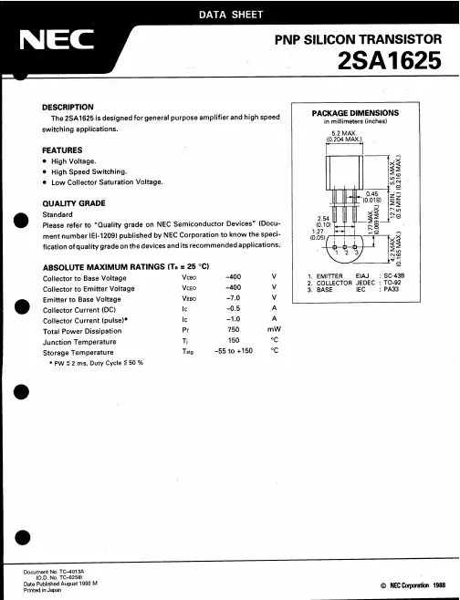
2SA1625中文资料
- 格式:pdf
- 大小:194.55 KB
- 文档页数:4
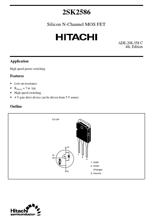
2SK2586Silicon N-Channel MOS FET
ADE-208-358 C4th. Edition
Application
High speed power switching
Features
• Low on-resistance
• RDS(on) = 7 m typ.
• High speed switching
• 4 V gate drive device can be driven from 5 V source
Outline
123TO-3P
1. Gate2. Drain (Flange)3. SourceD
G
S2SK2586
2Absolute Maximum Ratings (Ta = 25°C)
ItemSymbolRatingsUnit
Drain to source voltageVDSS60V
Gate to source voltageVGSS±20V
Drain currentID*260A
Drain peak currentID(pulse)*1240A
Body to drain diode reverse drain currentIDR*260A
Avalanche currentIAP*345A
Avalanche energyEAR*3174mJ
Channel dissipationPch*2125W
Channel temperatureTch150°C
Storage temperatureTstg–55 to +150°C
Notes:1.PW ≤ 10 µs, duty cycle ≤ 1 %2.Value at Tc = 25°C3.Value at Tch = 25°C, Rg ≥ 50 Ω2SK2586
3Electrical Characteristics (Ta = 25°C)
ItemSymbolMinTypMaxUnitTest Conditions
Drain to source breakdownvoltageV(BR)DSS60——VID = 10 mA, VGS = 0
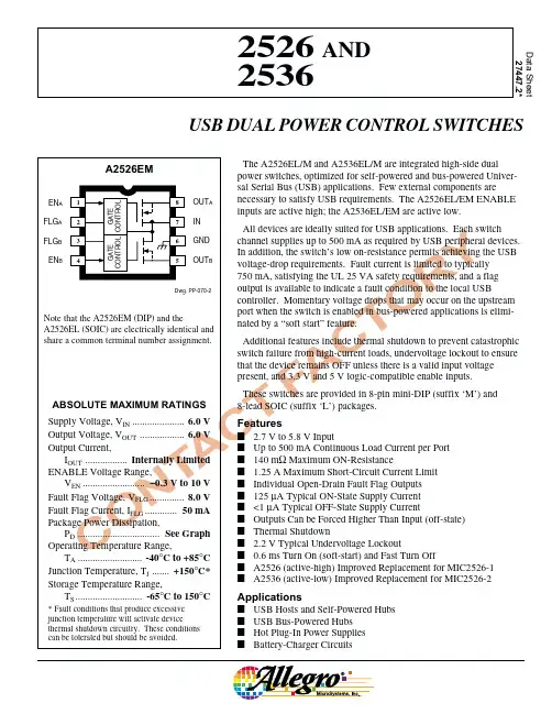
CONTACT FACTORYData Sheet27447.2*2526 AND2536USB DUAL POWER CONTROL SWITCHESA2526EM12345678ENAFLGAFLGBENBOUTAINGNDOUTBDwg. PP-070-2GATECONTROLGATECONTROLThe A2526EL/M and A2536EL/M are integrated high-side dualpower switches, optimized for self-powered and bus-powered Univer-sal Serial Bus (USB) applications. Few external components arenecessary to satisfy USB requirements. The A2526EL/EM ENABLEinputs are active high; the A2536EL/EM are active low.All devices are ideally suited for USB applications. Each switchchannel supplies up to 500 mA as required by USB peripheral devices.In addition, the switch’s low on-resistance permits achieving the USBvoltage-drop requirements. Fault current is limited to typically750 mA, satisfying the UL 25 VA safety requirements, and a flagoutput is available to indicate a fault condition to the local USBcontroller. Momentary voltage drops that may occur on the upstreamport when the switch is enabled in bus-powered applications is elimi-nated by a “soft start” feature.Additional features include thermal shutdown to prevent catastrophicswitch failure from high-current loads, undervoltage lockout to ensurethat the device remains OFF unless there is a valid input voltagepresent, and 3.3 V and 5 V logic-compatible enable inputs.These switches are provided in 8-pin mini-DIP (suffix ‘M’) and8-lead SOIC (suffix ‘L’) packages.FeaturesI2.7 V to 5.8 V InputIUp to 500 mA Continuous Load Current per PortI140 mΩ Maximum ON-ResistanceI1.25 A Maximum Short-Circuit Current LimitIIndividual Open-Drain Fault Flag OutputsI125 µA Typical ON-State Supply CurrentI<1 µA Typical OFF-State Supply CurrentIOutputs Can be Forced Higher Than Input (off-state)IThermal ShutdownI2.2 V Typical Undervoltage LockoutI0.6 ms Turn On (soft-start) and Fast Turn OffIA2526 (active-high) Improved Replacement for MIC2526-1IA2536 (active-low) Improved Replacement for MIC2526-2ApplicationsIUSB Hosts and Self-Powered HubsIUSB Bus-Powered HubsIHot Plug-In Power SuppliesIBattery-Charger CircuitsNote that the A2526EM (DIP) and theA2526EL (SOIC) are electrically identical andshare a common terminal number assignment.ABSOLUTE MAXIMUM RATINGSSupply Voltage, VIN..................... 6.0 VOutput Voltage, VOUT.................. 6.0 VOutput Current,IOUT................. Internally LimitedENABLE Voltage Range,VEN......................... –0.3 V to 10 VFault Flag Voltage, VFLG.............. 8.0 VFault Flag Current, IFLG............. 50 mAPackage Power Dissipation,PD................................. See GraphOperating Temperature Range,TA.......................... -40°C to +85°CJunction Temperature, TJ....... +150°C*Storage Temperature Range,TS........................... -65°C to 150°C* Fault conditions that produce excessivejunction temperature will activate devicethermal shutdown circuitry. These conditionscan be tolerated but should be avoided.元器件交易网115 Northeast Cutoff, Box 15036Worcester, Massachusetts 01615-0036 (508) 853-50002526 AND 2536USBDUAL POWER CONTROLSWITCHES
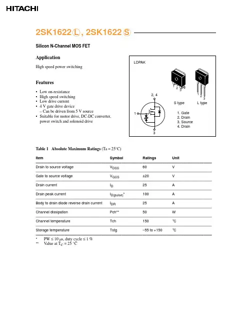
ApplicationHigh speed power switchingFeatures•Low on-resistance•High speed switching•Low drive current•4 V gate drive device– Can be driven from 5 V source•Suitable for motor drive, DC-DC converter,power switch and solenoid driveTable 1 Absolute Maximum Ratings (Ta = 25°C)ItemSymbolRatingsUnit———————————————————————————————————————————Drain to source voltageVDSS60V———————————————————————————————————————————Gate to source voltageVGSS±20V———————————————————————————————————————————Drain currentID25A———————————————————————————————————————————Drain peak currentID(pulse)*100A———————————————————————————————————————————Body to drain diode reverse drain currentIDR25A———————————————————————————————————————————Channel dissipationPch**50W———————————————————————————————————————————Channel temperatureTch150°C———————————————————————————————————————————Storage temperatureTstg–55 to +150°C———————————————————————————————————————————*PW ≤10 µs, duty cycle ≤1 %**Value at TC= 25 °C2SK1622 L, 2SK1622 SSilicon N-Channel MOS FET12

该SG3525A的脉宽调制器控制电路提供提高性能和降低外部元件数时实施了控制开关电源的所有类型。
片上5.1 V参考修剪成?1%的错误放大器的输入共模电压范围,包括参考电压,从而消除了对外部分压器的需求电阻。在同步输入到振荡器使多个单位以苦练或一个单位可以同步到一个外部系统时钟。广泛的死区时间可以由单个电阻器编程连接在CT和放电针。这个装置还带有内置软启动电路,只需要一个外部定时电容器。关断控制引脚同时软启动电路和输出级,瞬间又提供了通过脉宽调制锁存器脉冲关机,以及软启动回收与再关闭命令。根据输出电压锁定抑制和不断变化的软启动电容时的VCC低于有名无实。输出阶段的图腾柱设计能力的沉没并在200 mA的超额采购。该SG3525A的输出级在功能的NOR为关闭状态低产出导致逻辑。
特点
8.0 V至35 V工作电压
v1.0的5.1%,边参考
100赫兹至400赫兹振荡器范围
独立的振荡器同步引脚
可调节死区时间控制
输入欠压锁定
锁定的PWM脉冲,以防止多重
脉冲鈭抌Ÿ鈭扨ulse关机
双源/接收器输出:400 mA峰值
铅鈭扚稀土元素包现已推出*
PIN CONNECTIONS
Inv. Input
Sync
OSC. Output
RT
Discharge
Soft-Start
Noninv. Input
CT
Compensation
Shutdown
Output A
VC
Output B
VCC
Vref
Ground