
1N6314中文资料
- 格式:pdf
- 大小:97.48 KB
- 文档页数:2


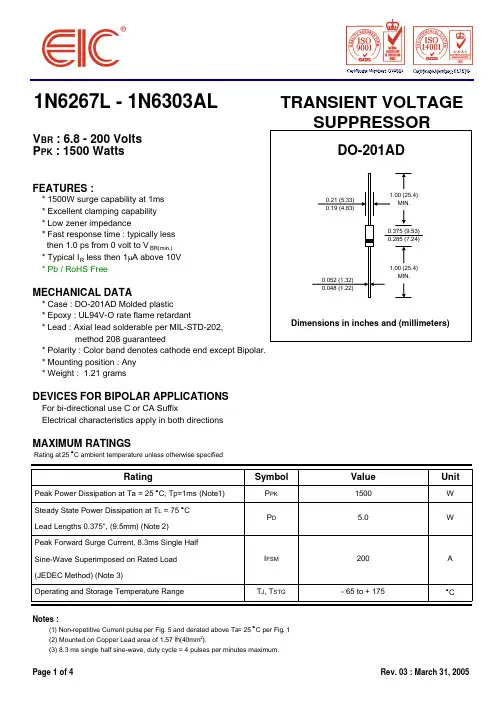
1N6267L - 1N6303ALTRANSIENT VOLTAGEVBR : 6.8 - 200 Volts P PK : 1500 WattsFEATURES :* 1500W surge capability at 1ms * Excellent clamping capability * Low zener impedance* Fast response time : typically less then 1.0 ps from 0 volt to V BR(min.) * Typical I R less then 1μA above 10V * Pb / RoHS FreeMECHANICAL DATA* Case : DO-201AD Molded plastic* Epoxy : UL94V-O rate flame retardant* Lead : Axial lead solderable per MIL-STD-202,method 208 guaranteed* Polarity : Color band denotes cathode end except Bipolar. * Mounting position : Any * Weight : 1.21 gramsDEVICES FOR BIPOLAR APPLICATIONSFor bi-directional use C or CA SuffixElectrical characteristics apply in both directionsMAXIMUM RATINGSRating at 25 °C ambient temperature unless otherwise specified .RatingSymbolValueUnitPeak Power Dissipation at Ta = 25 °C, Tp=1ms (Note1)P PK 1500W Steady State Power Dissipation at T L = 75 °C Lead Lengths 0.375", (9.5mm) (Note 2) Peak Forward Surge Current, 8.3ms Single Half Sine-Wave Superimposed on Rated Load (JEDEC Method) (Note 3)Operating and Storage Temperature Range T J , T STG - 65 to + 175°CNotes :(1) Non-repetitive Current pulse , per Fig. 5 and derated above Ta = 25 °C per Fig. 1(2) Mounted on Copper Lead area of 1.57 in 2 (40mm 2).(3) 8.3 ms single half sine-wave, duty cycle = 4 pulses per minutes maximum.Page 1 of 4Rev. 03 : March 31, 2005WAP DI FSM 2005.0ELECTRICAL CHARACTERISTICSRating at 25 °C ambient temperature unless otherwise specifiedBreakdown Voltage @ ItWorking Peak Maximum Maximum Maximum Maximum ( Note 1 )Reverse Reverse LeakageReverse Clamping Temperature Voltage @ V RWMCurrent Voltage @ I RSMCo-efficient V BR (V)It V RWM I R I RSM V RSM of V BR Min.Max.(mA)(V)(μA)(A)(V)(% / °C)1N6267L 6.127.4810 5.50100013910.80.057 1N6267AL 6.457.1410 5.80100014310.50.057 1N6268L 6.758.2510 6.0550012811.70.061 1N6268AL 7.137.88106.4050013211.30.061 1N6269L 7.389.0210 6.6320012012.50.065 1N6269AL 7.798.61107.022*******.10.065 1N6270L 8.1910.0 1.07.375010913.80.068 1N6270AL 8.659.55 1.07.785011213.40.068 1N6271L 9.0011.0 1.08.101010015.00.073 1N6271AL 9.5010.5 1.08.551010314.50.073 1N6272L 9.9012.1 1.08.92 5.093.016.20.075 1N6272AL 10.511.6 1.09.40 5.096.015.60.075 1N6273L 10.813.2 1.09.72 5.087.017.30.078 1N6273AL 11.412.6 1.010.2 5.090.016.70.078 1N6274L 11.714.3 1.010.5 5.079.019.00.081 1N6274AL 12.413.7 1.011.1 5.082.018.20.081 1N6275L 13.516.5 1.012.1 5.068.022.00.084 1N6275AL 14.315.8 1.012.8 5.071.021.20.084 1N6276L 14.417.6 1.012.9 5.064.023.50.086 1N6276AL 15.216.8 1.013.6 5.067.022.50.086 1N6277L 16.219.8 1.014.5 5.056.526.50.088 1N6277AL 17.118.9 1.015.3 5.059.525.20.088 1N6278L 18.022.0 1.016.2 5.051.529.10.090 1N6278AL 19.021.0 1.017.1 5.054.027.70.090 1N6279L 19.824.2 1.017.8 5.047.031.90.092 1N6279AL 20.923.1 1.018.8 5.049.030.60.092 1N6280L 21.626.4 1.019.4 5.043.034.70.094 1N6280AL 22.825.2 1.020.5 5.045.033.20.094 1N6281L 24.329.7 1.021.8 5.038.539.10.096 1N6281AL 25.728.4 1.023.1 5.040.037.50.096 1N6282L 27.033.0 1.024.3 5.034.543.50.097 1N6282AL 28.531.5 1.025.6 5.036.041.40.097 1N6283L 29.736.3 1.026.8 5.031.547.70.098 1N6283AL 31.434.7 1.028.2 5.033.045.70.098 1N6284L 32.439.6 1.029.1 5.029.052.00.099 1N6284AL 34.237.8 1.030.8 5.030.049.90.099 1N6285L 35.142.9 1.031.6 5.026.556.40.100 1N6285AL 37.141.0 1.033.3 5.028.053.90.100 1N6286L 38.747.3 1.034.8 5.024.061.90.101 1N6286AL 40.945.2 1.036.8 5.025.359.30.101 1N6287L 42.351.7 1.038.1 5.022.267.80.101 1N6287AL 44.749.4 1.040.2 5.023.264.80.101 1N6288L 45.956.1 1.041.3 5.020.473.50.102 1N6288AL48.553.61.043.65.021.470.10.102Page 2 of 4Rev. 03 : March 31, 2005TYPEELECTRICAL CHARACTERISTICSRating at 25 °C ambient temperature unless otherwise specifiedBreakdown Voltage @ ItWorking Peak Maximum Maximum Maximum Maximum ( Note 1 )Reverse Reverse LeakageReverse Clamping Temperature Voltage @ V RWMCurrent Voltage @ I RSMCo-efficient V BR (V)It V RWM I R I RSM V RSM of V BR Min.Max.(mA)(V)(μA)(A)(V)(% / °C)TYPE1N6289L50.461.6 1.045.4 5.018.680.50.103 1N6289AL 53.258.8 1.047.8 5.019.577.00.103 1N6290L 55.868.2 1.050.2 5.016.989.00.104 1N6290AL 58.965.1 1.053.05.017.785.00.104 1N6291L 61.274.8 1.055.1 5.015.398.00.104 1N6291AL 64.671.4 1.058.1 5.016.392.00.104 1N6292L 67.582.5 1.060.7 5.013.91080.105 1N6292AL 71.378.8 1.064.1 5.014.61030.105 1N6293L 73.890.2 1.066.4 5.012.71180.105 1N6293AL 77.986.1 1.070.1 5.013.31130.105 1N6294L 81.9100 1.073.7 5.011.41310.106 1N6294AL 86.595.5 1.077.8 5.012.01250.106 1N6295L 90.0110 1.081.0 5.010.41440.106 1N6295AL 95.0105 1.085.5 5.011.01370.106 1N6296L 99.0121 1.089.2 5.09.51580.107 1N6296AL 105116 1.094.0 5.09.91520.107 1N6297L 108132 1.097.2 5.08.71730.107 1N6297AL 114126 1.0102 5.09.11650.107 1N6298L 117143 1.0105 5.08.01870.107 1N6298AL 124137 1.0111 5.08.41790.107 1N6299L 135165 1.0121 5.07.02150.108 1N6299AL 143158 1.0128 5.07.22070.108 1N6300L 144176 1.0130 5.0 6.52300.108 1N6300AL 152168 1.0136 5.0 6.82190.108 1N6301L 153187 1.0138 5.0 6.22440.108 1N6301AL 162179 1.0145 5.0 6.42340.108 1N6302L 162198 1.0146 5.0 5.82580.108 1N6302AL 171189 1.0154 5.0 6.12460.108 1N6303L 180220 1.0162 5.0 5.22870.108 1N6303AL1902101.01715.05.52740.108Note:( 1 ) V BR measured after It applied for 300μs., It = square wave pulse or equivalen ( 2 ) V F = 3.5 Vmax., I F = 100 Amps. ( 6.8 Volts thru 91 Volts )V F = 5.0 Vmax., I F = 100 Amps. ( 100 Volts thru 200 Volts ) per 1/2square or equivalent sine wave PW = 8.3 ms, duty cycle = 4 pulses per minute maximumPage 3 of 4Rev. 03 : March 31, 2005Page 4 of 4Rev. 03 : March 31, 2005。

6N134中⽂资料FeaturesDual Marked with Device Part Number and DSCC Drawing NumberManufactured and Tested on a MIL-PRF-38534 Certified LineQML-38534, Class H and K Five Hermetically Sealed Package Configurations Performance Guaranteed over -55°C to +125°C ? High Speed: 10 M Bit/sCMR: > 10,000 V/µs Typical 1500 Vdc Withstand Test Voltage2500 Vdc Withstand Test Voltage for HCPL-565X High Radiation Immunity 6N137, HCPL-2601, HCPL-2630/-31 Function Compatibility ? Reliability DataTTL Circuit CompatibilityApplicationsMilitary and SpaceHigh Reliability SystemsTransportation, Medical, and Life Critical SystemsLine ReceiverVoltage Level ShiftingIsolated Input Line Receiver Isolated Output Line Driver Logic Ground Isolation Harsh Industrial EnvironmentsIsolation for Computer,Communication, and Test Equipment SystemsDescriptionThese units are single, dual and quad channel, hermetically sealed optocouplers. The products are capable of operation and storage over the full military temperature range and can be purchased as either standard product or with full MIL-PRF-38534 Class Level H or K testing or from the appropri-ate DSCC Drawing. All devices are manufactured and tested on a MIL-PRF-38534 certified line and are included in the DSCC Quali-fied Manufacturers List QML-38534 for Hybrid Microcircuits.Quad channel devices areavailable by special order in the 16 pin DIP through hole packages.Truth Table(Positive Logic)Multichannel DevicesInput Output On (H)L Off (L)HFunctional DiagramMultiple Channel Devices AvailableSingle Channel DIP Input Enable Output On (H)H L Off (L)H H On (H)L H Off (L)LH*See matrix for available extensions.Hermetically Sealed, High Speed,High CMR, Logic Gate Optocouplers Technical Data6N134*81028HCPL-563X HCPL-663X HCPL-565X 5962-98001HCPL-268K HCPL-665X 5962-90855HCPL-560XCAUTION: It is advised that normal static precautions be taken in handling and assembly of this component to prevent damage and/or degradation which may be induced by ESD.V CC V OUTV E GNDThe connection of a 0.1 µF bypass capacitor between V CC and GND is recommended.Selection Guide–Package Styles and Lead Configuration OptionsPackage16 Pin DIP 8 Pin DIP 8 Pin DIP 8 Pin DIP 16 Pin Flat Pack 20 Pad LCCC Lead Style Through Hole Through Hole Through Hole Through Hole Unformed Leads Surface MountChannels 212242Common Channel V CC , GND None V CC , GND V CC , GND V CC , GND None WiringWithstand Test Voltage 1500 Vdc 1500 Vdc 1500 Vdc 2500 Vdc 1500 Vdc 1500 Vdc Agilent Part # & Options Commercial6N134*HCPL-5600HCPL-5630HCPL-5650HCPL-6650HCPL-6630MIL-PRF-38534, Class H 6N134/883BHCPL-5601HCPL-5631HCPL-5651HCPL-6651HCPL-6631MIL-PRF-38534, Class K HCPL-268K HCPL-560K HCPL-563K HCPL-665K HCPL-663K Standard Lead Finish Gold Plate Gold Plate Gold Plate Gold Plate Gold PlateSolder PadsSolder Dipped Option #200Option #200Option #200Option #200Butt Cut/Gold Plate Option #100Option #100Option #100Gull Wing/Soldered Option #300Option #300Option #300Class H SMD Part #Prescript for all below None 5962-None None None None Either Gold or Solder 8102801EX 9085501HPX 8102802PX 8102805PX 8102804FX 81028032XGold Plate 8102801EC 9085501HPC 8102802PC 8102805PC 8102804FCSolder Dipped 8102801EA 9085501HPA 8102802PA 8102805PA81028032A Butt Cut/Gold Plate 8102801UC 9085501HYC 8102802YC Butt Cut/Soldered 8102801UA 9085501HYA 8102802YA Gull Wing/Soldered 8102801TA 9085501HXA8102802ZA Class K SMD Part #Prescript for all below 5962-5962-5962-5962-5962-Either Gold or Solder 9800101KEX 9085501KPX 9800102KPX 9800104KFX 9800103K2XGold Plate 9800101KEC 9085501KPC 9800102KPC 9800104KFCSolder Dipped 9800101KEA 9085501KPA 9800102KPA 9800103K2AButt Cut/Gold Plate 9800101KUC 9085501KYC 9800102KYC Butt Cut/Soldered 9800101KUA 9085501KYA 9800102KYA Gull Wing/Soldered9800101KTA 9085501KXA 9800102KZA*JEDEC registered part.Each channel contains a GaAsP light emitting diode which isoptically coupled to an integrated high speed photon detector. The output of the detector is an open collector Schottky clamped transistor. Internal shields provide a guaranteed common mode transient immunityspecification of 1000 V/µs. For Isolation Voltage applications requiring up to 2500 Vdc, the HCPL-5650 family is also available. Package styles for these parts are 8 and 16 pin DIP through hole (case outlines P andE respectively), and 16 pin surface mount DIP flat pack(case outline F), leadless ceramic chip carrier (case outline 2).Devices may be purchased with a variety of lead bend and plating options. See Selection Guide Table for details. Standard Microcircuit Drawing (SMD)parts are available for each package and lead style.Because the same electrical die (emitters and detectors) are used for each channel of each device listed in this data sheet, absolute maximum ratings, recommended operating conditions, electrical specifications, and performance characteristics shown in the figures are identical for all parts.Occasional exceptions exist due to package variations and limitations,and are as noted. Additionally, the same package assembly processes and materials are used in all devices. These similarities give justification for the use of data obtained from one part torepresent other parts’ performance for reliability and certain limited radiation test results.Outline Drawings16 Pin DIP Through Hole, 2 ChannelsFunctional DiagramsNote: All DIP and flat pack devices have common V CC and ground. Single channel DIP has an enable pin 7. LCCC (leadless ceramic chip carrier) package has isolated channels with separate VCC and ground connections. All diagrams are “top view.”Leaded Device MarkingLeadless Device MarkingNOTE: DIMENSIONS IN MILLIMETERS (INCHES).COMPLIANCE INDICATOR,*DATE CODE, SUFFIX (IF NEEDED)COUNTRY OF MFR.Agilent CAGE CODE*Agilent DESIGNATORDSCC SMD*PIN ONE/ ESD IDENTAgilent P/N DSCC SMD** QUALIFIED PARTS ONLYCOMPLIANCE INDICATOR,*DATE CODE, SUFFIX (IF NEEDED)DSCC SMD*Agilent CAGE CODE*Agilent DESIGNATORCOUNTRY OF MFR.Agilent P/N PIN ONE/ ESD IDENTDSCC SMD** QUALIFIED PARTS ONLYOutline Drawings (continued)16 Pin Flat Pack, 4 Channels8 Pin DIP Through Hole, 2 Channels 2500 Vdc Withstand Test Voltage20 Terminal LCCC Surface Mount,2Channels8 Pin DIP Through Hole, 1 and 2 Channels0.36 (0.014)NOTE: DIMENSIONS IN MILLIMETERS (INCHES).2.29 (0.090) 2.79 (0.110)NOTE: DIMENSIONS IN MILLIMETERS (INCHES).NOTE: DIMENSIONS IN MILLIMETERS (INCHES).NOTE: DIMENSIONS IN MILLIMETERS (INCHES). SOLDER THICKNESS 0.127 (0.005) MAX.Hermetic Optocoupler OptionsRecommended Operating ConditionsParameterSymbol Min.Max.Units Input Current, Low Level, Each Channel I FL 0250µA Input Current, High Level, Each Channel*I FH 1020mA Supply Voltage, OutputV CC 4.55.5VFan Out (TTL Load) Each ChannelN6*Meets or exceeds DSCC SMD and JEDEC requirements.Absolute Maximum Ratings(No derating required up to +125°C)Storage Temperature Range, T S ...................................-65°C to +150°C Operating Temperature, T A..........................................-55°C to +125°C Case Temperature, T C ................................................................+170°C Junction Temperature, T J ...........................................................+175°C Lead Solder Temperature ...............................................260°C for 10 s Peak Forward Input Current, I F PK , (each channel,≤1 ms duration)......................................................................40 mA Average Input Forward Current, I F AVG (each channel)................20 mA Input Power Dissipation (each channel).....................................35 mW Reverse Input Voltage, V R (each channel).........................................5 V Supply Voltage, V CC (1 minute maximum)........................................7 V Output Current, I O (each channel)...............................................25 mA Output Power Dissipation (each channel). (40)mW Output Voltage, V O (each channel)..................................................7 V*Package Power Dissipation, P D (each channel)........................200 mW*Selection for higher output voltages up to 20 V is available.Single Channel Product OnlyEmitter Input Voltage, V E ...............................................................5.5 VNote enable pin 7. An external 0.01 µF to 0.1 µF bypass capacitor must be connected between V CC and ground for each package type.8 Pin Ceramic DIP Single Channel SchematicESD Classification(MIL-STD-883, Method 3015)HCPL-5600/01/0K ...............................................................(?), Class 16N134, 6N134/883B, HCPL-5630/31/3K, HCPL-5650/51, HCPL-6630/31/3K and HCPL-6650/51/5K.......................(Dot), Class 3Electrical Characteristics (T= -55°C to +125°C, unless otherwise specified)*Identified test parameters for JEDEC registered parts.**All typical values are at V CC = 5 V , T A = 25°C. Recommended Operating Conditions (cont’d.)Single Channel Product Only [10]ParameterSymbol Min.Max.Units High Level Enable Voltage V EH 2.0V CC V Low Level Enable VoltageV EL0.8VElectrical Characteristics, (Contd.) T= -55°C to +125°C unless otherwise specifiedSingle Channel Product Only Low Level I EL V CC = 5.5 V,1, 2, 3-1.45-2.0mA Enable Current V E = 0.5 V High Level V EH 1, 2, 3 2.0V10Enable Voltage Low Level V EL 1, 2, 30.8VEnable Voltage*Identified test parameters for JEDEC registered part.**All typical values are at V CC = 5 V , T A = 25°C.Typical Characteristics, T = 25°C, V = 5 VDual and Quad Channel Product Only Input-Input I I-I 0.5nA Relative Humidity = 45%4Leakage CurrentV I-I = 500 V, t = 5 s Resistance (Input-Input)R I-I 1012V I-I = 500 V 4Capacitance (Input-Input)C I-I0.55pF f = 1 MHz4Notes:1. Each channel.2. All devices are considered two-terminal devices; I I-O is measured between all input leads or terminals shorted together and alloutput leads or terminals shorted together.3. Measured between each input pair shorted together and all output connections for that channel shorted together.4. Measured between adjacent input pairs shorted together for each multichannel device.5. t PHL propagation delay is measured from the 50% point on the leading edge of the input pulse to the 1.5 V point on the leadingedge of the output pulse. The t PLH propagation delay is measured from the 50% point on the trailing edge of the input pulse to the1.5 V point on the trailing edge of the output pulse.6. The HCPL-6630, HCPL-6631, and HCPL-663K dual channel parts function as two independent single channel units. Use the singlechannel parameter limits for each channel.7. CM L is the maximum rate of rise of the common mode voltage that can be sustained with the output voltage in the logic low state(V O < 0.8 V). CM H is the maximum rate of fall of the common mode voltage that can be sustained with the output voltage in the logic high state (V O > 2.0 V).8. This is a momentary withstand test, not an operating condition.9. It is essential that a bypass capacitor (0.01 to 0.1 µF, ceramic) be connected from V CC to ground. Total lead length between bothends of this external capacitor and the isolator connections should not exceed 20 mm.10. No external pull up is required for a high logic state on the enable input.11. The t ELH enable propagation delay is measured from the 1.5 V point on the trailing edge of the enable input pulse to the 1.5 Vpoint on the trailing edge of the output pulse.12. The t EHL enable propagation delay is measured from the 1.5 V point on the leading edge of the enable input pulse tothe 1.5 Vpoint on the leading edge of the output pulse.13. Standard parts receive 100% testing at 25°C (Subgroups 1 and 9). SMD and 883B parts receive 100% testing at 25, 125, and-55°C (Subgroups 1 and 9, 2 and 10, 3 and 11, respectively).14. Parameters are tested as part of device initial characterization and after design and process changes. Parameters are guaranteedto limits specified for all lots not specifically tested.15. Not required for 6N134, 6N134/883B, 8102801, HCPL-268K and 5962-9800101 types.16. Required for 6N134, 6N134/883B, 8102801, HCPL-268K and 5962-9800101 types.17. Not required for HCPL-5650, HCPL-5651 and 8102805 types.18. Required for HCPL-5650, HCPL-5651 and 8102805 types only.Figure 1. High Level Output Currentvs. Temperature.5 VV O * C L INCLUDES PROBE AND STRAY WIRING CAPACITANCE. Figure 4. Test Circuit for t PHL and t PLH .*I +5 V OUTPUT V O MONITORING NODEFigure 7. Test Circuit for Common Mode Transient Immunity and Typical Waveforms.11OUTPUT V OMONITORINGNODET A = +125 °C* ALL CHANNELS TESTED SIMULTANEOUSLY.V CCI O = 25 mAFigure 10. Operating Circuit for Burn-In and Steady State Life Tests. Figure 8. Test Circuit for t EHL and t ELH.Figure 9. Enable Propagation Delayvs. Temperature.MIL-PRF-38534 Class H,Class K, and DSCC SMDTest ProgramAgilent’s Hi-Rel Optocouplers arein compliance with MIL-PRF-38534 Classes H and K. Class Hand Class K devices are also incompliance with DSCC drawings81028, 5962-90855 and 5962-98001.Testing consists of 100% screen-ing and quality conformanceinspection to MIL-PRF-38534./doc/4e2d970a03d8ce2f006623a8.htmlData subject to change.Copyright ? 1999 Agilent TechnologiesObsoletes 5968-4743E5968-9407E (10/00)。