
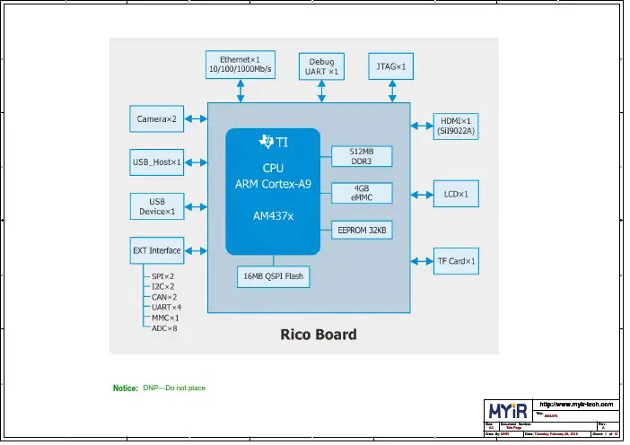
Rico Board_schematic_RevA
- 格式:pdf
- 大小:220.31 KB
- 文档页数:12
SP601 Hardware User GuideUG518 (v1.7) September 26, 2012© Copyright 2009–2012 Xilinx, Inc. Xilinx, the Xilinx logo, Artix, ISE, Kintex, Spartan, Virtex, Zynq, and other designated brands included herein are trademarks of Xilinx in the United States and other countries. All other trademarks are the property of their respective owners. DISCLAIMERThe information disclosed to you hereunder (the “Materials”) is provided solely for the selection and use of Xilinx products. To the maximum extent permitted by applicable law: (1) Materials are made available “AS IS” and with all faults, Xilinx hereby DISCLAIMS ALL WARRANTIES AND CONDITIONS, EXPRESS, IMPLIED, OR ST ATUTORY, INCLUDING BUT NOT LIMITED TO WARRANTIES OF MERCHANTABILITY, NON-INFRINGEMENT, OR FITNESS FOR ANY PARTICULAR PURPOSE; and (2) Xilinx shall not be liable (whether in contract or tort, including negligence, or under any other theory of liability) for any loss or damage of any kind or nature related to, arising under, or in connection with, the Materials (including your use of the Materials), including for any direct, indirect, special, incidental, or consequential loss or damage (including loss of data, profits, goodwill, or any type of loss or damage suffered as a result of any action brought by a third party) even if such damage or loss was reasonably foreseeable or Xilinx had been advised of the possibility of the same. Xilinx assumes no obligation to correct any errors contained in the Materials, or to advise you of any corrections or update. Y ou may not reproduce, modify, distribute, or publicly display the Materials without prior written consent. Certain products are subject to the terms and conditions of the Limited Warranties which can be viewed at /warranty.htm; IP cores may be subject to warranty and support terms contained in a license issued to you by Xilinx. Xilinx products are not designed or intended to be fail-safe or for use in any application requiring fail-safe performance; you assume sole risk and liability for use of Xilinx products in Critical Applications:/warranty.htm#critapps.Revision HistoryThe following table shows the revision history for this document.Date Version Revision07/15/09 1.0Initial Xilinx release.08/19/09 1.1•Added Appendix B, VITA 57.1 FMC LPC Connector Pinout.•Updated Figure1-17.•Updated Table1-4, Table1-19, and Table1-22.•Added introductory paragraph to Appendix C, SP601 Master UCF.•Miscellaneous typographical edits and new user guide template.05/17/10 1.2•Updated Figure1-1, Figure1-2, Figure1-14, Figure1-18, Table1-9, Table1-1,Table1-11, and Table1-16.•Added Figure1-7, Figure1-8, and Table1-13.•Updated 9. VITA 57.1 FMC-LPC Connector, page25, Appendix B, VITA 57.1 FMCLPC Connector Pinout, and Appendix C, SP601 Master UCF.06/16/10 1.3Reversed order of 15. Configuration Options and 16. Power Management. Updated 1.Spartan-6 XC6SLX16-2CSG324 FPGA and 2. 128 MB DDR2 Component Memory. AddedTable1-26. Added UG394, Spartan-6 FPGA Power Management User Guide to Appendix D,References.09/24/10 1.4Added Power System Test Points, including Table1-25.02/16/11 1.5Added note and revised header description to indicate the I/Os support LVCMOS25signaling on page34. Revised oscillator manufacturer information from Epson to SiTimeon page page23 and page51.07/18/11 1.6Corrected wording from “PPM frequency jitter” to “PPM frequency stability” in sectionOscillator (Differential), page23. Added Table1-15, page27.09/26/12 1.7Added Regulatory and Compliance Information, page53.SP601 Hardware User Guide UG518 (v1.7) September 26, 2012SP601 Hardware User Guide 3UG518 (v1.7) September 26, 2012Revision History . . . . . . . . . . . . . . . . . . . . . . . . . . . . . . . . . . . . . . . . . . . . . . . . . . . . . . . . . . . . . 2Preface: About This GuideGuide Contents . . . . . . . . . . . . . . . . . . . . . . . . . . . . . . . . . . . . . . . . . . . . . . . . . . . . . . . . . . . . . . 5Additional Documentation . . . . . . . . . . . . . . . . . . . . . . . . . . . . . . . . . . . . . . . . . . . . . . . . . . . 5Additional Support Resources . . . . . . . . . . . . . . . . . . . . . . . . . . . . . . . . . . . . . . . . . . . . . . . . 6Chapter 1: SP601 Evaluation BoardOverview . . . . . . . . . . . . . . . . . . . . . . . . . . . . . . . . . . . . . . . . . . . . . . . . . . . . . . . . . . . . . . . . . . . . 7Additional Information. . . . . . . . . . . . . . . . . . . . . . . . . . . . . . . . . . . . . . . . . . . . . . . . . . . . . 7Features . . . . . . . . . . . . . . . . . . . . . . . . . . . . . . . . . . . . . . . . . . . . . . . . . . . . . . . . . . . . . . . . . . 8Block Diagram . . . . . . . . . . . . . . . . . . . . . . . . . . . . . . . . . . . . . . . . . . . . . . . . . . . . . . . . . . . . 9Related Xilinx Documents . . . . . . . . . . . . . . . . . . . . . . . . . . . . . . . . . . . . . . . . . . . . . . . . . . . . 9Detailed Description . . . . . . . . . . . . . . . . . . . . . . . . . . . . . . . . . . . . . . . . . . . . . . . . . . . . . . . . 101. Spartan-6 XC6SLX16-2CSG324 FPGA. . . . . . . . . . . . . . . . . . . . . . . . . . . . . . . . . . . . . . 11Configuration . . . . . . . . . . . . . . . . . . . . . . . . . . . . . . . . . . . . . . . . . . . . . . . . . . . . . . . . . 11I/O Voltage Rails . . . . . . . . . . . . . . . . . . . . . . . . . . . . . . . . . . . . . . . . . . . . . . . . . . . . . . 122. 128 MB DDR2 Component Memory . . . . . . . . . . . . . . . . . . . . . . . . . . . . . . . . . . . . . . . 123. SPI x4 Flash . . . . . . . . . . . . . . . . . . . . . . . . . . . . . . . . . . . . . . . . . . . . . . . . . . . . . . . . . . . . 154. Linear Flash BPI . . . . . . . . . . . . . . . . . . . . . . . . . . . . . . . . . . . . . . . . . . . . . . . . . . . . . . . . 175. 10/100/1000 Tri-Speed Ethernet PHY . . . . . . . . . . . . . . . . . . . . . . . . . . . . . . . . . . . . . 196. USB-to-UART Bridge. . . . . . . . . . . . . . . . . . . . . . . . . . . . . . . . . . . . . . . . . . . . . . . . . . . . 217. IIC Bus . . . . . . . . . . . . . . . . . . . . . . . . . . . . . . . . . . . . . . . . . . . . . . . . . . . . . . . . . . . . . . . . 228-Kb NV Memory . . . . . . . . . . . . . . . . . . . . . . . . . . . . . . . . . . . . . . . . . . . . . . . . . . . . . . 228. Clock Generation . . . . . . . . . . . . . . . . . . . . . . . . . . . . . . . . . . . . . . . . . . . . . . . . . . . . . . . 23Oscillator (Differential). . . . . . . . . . . . . . . . . . . . . . . . . . . . . . . . . . . . . . . . . . . . . . . . . . 23Oscillator Socket (Single-Ended, 2.5V or 3.3V) . . . . . . . . . . . . . . . . . . . . . . . . . . . . . . . . 24SMA Connectors (Differential). . . . . . . . . . . . . . . . . . . . . . . . . . . . . . . . . . . . . . . . . . . . 249. VITA 57.1 FMC-LPC Connector . . . . . . . . . . . . . . . . . . . . . . . . . . . . . . . . . . . . . . . . . . 2510. Status LEDs. . . . . . . . . . . . . . . . . . . . . . . . . . . . . . . . . . . . . . . . . . . . . . . . . . . . . . . . . . . 2811. FPGA Awake LED and Suspend Jumper. . . . . . . . . . . . . . . . . . . . . . . . . . . . . . . . . . 2912. FPGA INIT and DONE LEDs. . . . . . . . . . . . . . . . . . . . . . . . . . . . . . . . . . . . . . . . . . . . 3013. User I/O . . . . . . . . . . . . . . . . . . . . . . . . . . . . . . . . . . . . . . . . . . . . . . . . . . . . . . . . . . . . . 3114. FPGA_PROG_B Pushbutton Switch . . . . . . . . . . . . . . . . . . . . . . . . . . . . . . . . . . . . . . 3515. Configuration Options . . . . . . . . . . . . . . . . . . . . . . . . . . . . . . . . . . . . . . . . . . . . . . . . . 36JTAG Configuration . . . . . . . . . . . . . . . . . . . . . . . . . . . . . . . . . . . . . . . . . . . . . . . . . . . . 3616. Power Management. . . . . . . . . . . . . . . . . . . . . . . . . . . . . . . . . . . . . . . . . . . . . . . . . . . . 37AC Adapter and 5V Input Power Jack/Switch . . . . . . . . . . . . . . . . . . . . . . . . . . . . . . . . 37Onboard Power Supplies . . . . . . . . . . . . . . . . . . . . . . . . . . . . . . . . . . . . . . . . . . . . . . . . 37Power System Test Points . . . . . . . . . . . . . . . . . . . . . . . . . . . . . . . . . . . . . . . . . . . . . . . . 38Table of ContentsAppendix A: Default Jumper and Switch SettingsAppendix B: VITA 57.1 FMC LPC Connector PinoutAppendix C: SP601 Master UCFAppendix D: ReferencesAppendix E: Regulatory and Compliance InformationDirectives. . . . . . . . . . . . . . . . . . . . . . . . . . . . . . . . . . . . . . . . . . . . . . . . . . . . . . . . . . . . . . . . . . . 53Standards. . . . . . . . . . . . . . . . . . . . . . . . . . . . . . . . . . . . . . . . . . . . . . . . . . . . . . . . . . . . . . . . . . . 53 Electromagnetic Compatibility . . . . . . . . . . . . . . . . . . . . . . . . . . . . . . . . . . . . . . . . . . . . . 53Safety . . . . . . . . . . . . . . . . . . . . . . . . . . . . . . . . . . . . . . . . . . . . . . . . . . . . . . . . . . . . . . . . . . . 53 Markings . . . . . . . . . . . . . . . . . . . . . . . . . . . . . . . . . . . . . . . . . . . . . . . . . . . . . . . . . . . . . . . . . . . 54 SP601 Hardware User GuideUG518 (v1.7) September 26, 2012SP601 Hardware User Guide 5UG518 (v1.7) September 26, 2012PrefaceAbout This GuideThis manual accompanies the Spartan®-6 FPGA SP601 Evaluation Board and contains information about the SP601 hardware and software tools.Guide ContentsThis manual contains the following chapters:•Chapter 1, SP601 Evaluation Board , provides an overview of the SP601 evaluation board and details the components and features of the SP601 board.•Appendix A, Default Jumper and Switch Settings .•Appendix B, VITA 57.1 FMC LPC Connector Pinout .•Appendix C, SP601 Master UCF .•Appendix D, References .Additional DocumentationThe following documents are available for download at /products/spartan6.•Spartan-6 Family OverviewThis overview outlines the features and product selection of the Spartan-6 family.•Spartan-6 FPGA Data Sheet: DC and Switching CharacteristicsThis data sheet contains the DC and switching characteristic specifications for the Spartan-6 family.•Spartan-6 FPGA Packaging and Pinout SpecificationsThis specification includes the tables for device/package combinations and maximum I/Os, pin definitions, pinout tables, pinout diagrams, mechanical drawings, and thermal specifications.•Spartan-6 FPGA Configuration User GuideThis all-encompassing configuration guide includes chapters on configuration interfaces (serial and parallel), multi-bitstream management, bitstream encryption, boundary-scan and JTAG configuration, and reconfiguration techniques.•Spartan-6 FPGA SelectIO Resources User GuideThis guide describes the SelectIO™ resources available in all Spartan-6 devices.•Spartan-6 FPG A Clocking Resources User GuidePreface:About This GuideThis guide describes the clocking resources available in all Spartan-6 devices,including the DCMs and PLLs.•Spartan-6 FPGA Block RAM Resources User GuideThis guide describes the Spartan-6 device block RAM capabilities.•Spartan-6 FPGA DSP48A1 Slice User GuideThis guide describes the architecture of the DSP48A1 slice in Spartan-6FPGAs andprovides configuration examples.•Spartan-6 FPGA Memory Controller User GuideThis guide describes the Spartan-6 FPGA memory controller block, a dedicatedembedded multi-port memory controller that greatly simplifies interfacingSpartan-6FPGAs to the most popular memory standards.•Spartan-6 FPGA PCB Designer’s GuideThis guide provides information on PCB design for Spartan-6 devices, with a focus onstrategies for making design decisions at the PCB and interface level.Additional Support ResourcesTo search the database of silicon and software questions and answers or to create atechnical support case in WebCase, see the Xilinx website at:/support. SP601 Hardware User GuideUG518 (v1.7) September 26, 2012Chapter1 SP601 Evaluation BoardOverviewThe SP601 board enables hardware and software developers to create or evaluate designstargeting the Spartan®-6 XC6SLX16-2CSG324 FPGA.The SP601 provides board features for evaluating the Spartan-6 family that are common tomost entry-level development environments. Some commonly used features include aDDR2 memory controller, a parallel linear flash, a tri-mode Ethernet PHY, general-purposeI/O (GPIO), and a UART. Additional functionality can be added through the VITA 57.1.1expansion connector. Features, page8 provides a general listing of the board features withdetails provided in Detailed Description, page10.Additional InformationAdditional information and support material is located at:•/sp601This information includes:•Current version of this user guide in PDF format•Example design files for demonstration of Spartan-6 FPGA features and technology•Demonstration hardware and software configuration files for the SP601 linear and SPImemory devices•Reference Design Files•Schematics in PDF format and DxDesigner schematic format•Bill of materials (BOM)•Printed-circuit board (PCB) layout in Allegro PCB format•Gerber files for the PCB (Many free or shareware Gerber file viewers are available onthe internet for viewing and printing these files.)•Additional documentation, errata, frequently asked questions, and the latest newsFor information about the Spartan-6 family of FPGA devices, including product highlights,data sheets, user guides, and application notes, see the Spartan-6 FPGA website at/support/documentation/spartan-6.htm.SP601 Hardware User Guide 7 UG518 (v1.7) September 26, 2012Chapter 1:SP601 Evaluation BoardFeaturesThe SP601 board provides the following features (see Figure1-2 and Table1-1):• 1. Spartan-6 XC6SLX16-2CSG324 FPGA• 2. 128 MB DDR2 Component Memory• 3. SPI x4 Flash• 4. Linear Flash BPI• 5. 10/100/1000 Tri-Speed Ethernet PHY•7. IIC Bus•8Kb NV memory•External access 2-pin header•VITA 57.1 FMC-LPC connector•8. Clock Generation•Oscillator (Differential)•Oscillator Socket (Single-Ended, 2.5V or 3.3V)•SMA Connectors (Differential)•9. VITA 57.1 FMC-LPC Connector•10. Status LEDs•FPGA_AWAKE•INIT•DONE•13. User I/O•User LEDs•User DIP switch•User pushbuttons•GPIO male pin header•14. FPGA_PROG_B Pushbutton Switch•15. Configuration Options• 3. SPI x4 Flash (both onboard and off-board)• 4. Linear Flash BPI•JTAG Configuration•16. Power Management•AC Adapter and 5V Input Power Jack/Switch•Onboard Power Supplies SP601 Hardware User GuideUG518 (v1.7) September 26, 2012Related Xilinx DocumentsBlock DiagramFigure1-1 shows a high-level block diagram of the SP601 and its peripherals.Figure 1-1:SP601 Features and BankingRelated Xilinx DocumentsPrior to using the SP601 Evaluation Board, users should be familiar with Xilinx resources.See the following locations for additional documentation on Xilinx tools and solutions:•ISE: /ise•Answer Browser: /support•Intellectual Property: /ipcenterSP601 Hardware User Guide 9 UG518 (v1.7) September 26, 2012SP601 Hardware User GuideUG518 (v1.7) September 26, 2012Chapter 1:SP601 Evaluation BoardDetailed DescriptionFigure 1-2 shows a board photo with numbered features corresponding to Table 1-1 and the section headings in this document.The numbered features in Figure 1-2 correlate to the features and notes listed in Table 1-1.Figure 1-2:SP601 Board PhotoUG518_02_09100912843126137115109141581316Table 1-1:SP601 FeaturesNumberFeatureNotesSchematic Page1 Spartan-6 FP G A XC6SLX16-2CS G 3242DDR2 Component Elpida EDE1116ACBG 1Gb DDR2SDRAM53SPI x4 Flash and Headers SPI select and External Headers 84Linear Flash BPIStrataFlash 8-bit (J3 device), 3 pins shared w/ SPI x481. Spartan-6 XC6SLX16-2CSG 324 FPGAA Xilinx Spartan-6 XC6SLX16-2CSG324 FPGA is installed on the SP601 Evaluation Board.ReferencesSee the Spartan-6 FPGA Data Sheet . [Ref 1]ConfigurationThe SP601 supports configuration in the following modes:•Master SPI x4•Master SPI x4 with off-board device •BPI•JTAG (using the included USB-A to Mini-B cable)For details on configuring the FPGA, see 15. Configuration Options .The Mode DIP switch SW2 is set to M[1:0] = 01 Master SPI default.ReferencesSee the Spartan-6 FPGA Configuration User Guide for more information. [Ref 2]510/100/1000 Ethernet PHY GMII Marvell Alaska PHY76RS232 UART (USB Bridge)Uses CP2103 Serial-to-USB connection 107IICGoes to Header and VITA 57.1 FMC 108Clock, socket, SMA Differential, Single-Ended, Differential 99VITA 57.1 FMC-LPC connector LVDS signals, clocks, PRSNT 610LEDs Ethernet PHY Status711LED, Header FPGA Awake LED, Suspend Header 812LEDs FPGA INIT, DONE 913LED User I/O (active-High)9DIP SwitchUser I/O (active-High)9PushbuttonUser I/O, CPU_RESET (active-High)912-pin (8 I/O) Header6 pins x 2 male header with 8 I/Os (active-High)1014Pushbutton FPGA_PROG_B915USB JTAG Cypress USB to JTAG download cable logic14, 1516Onboard PowerPower Management11,12,13Table 1-1:SP601 Features (Cont’d)NumberFeatureNotesSchematic PageSP601 Hardware User Guide I/O Voltage RailsThere are four available banks on the LX16-CSG324 device. Banks 0, 1, and 2 are connected for 2.5V I/O. Bank 3 is used for the 1.8V DDR2 component memory interface of Spartan-6 FPGA’s hard memory controller. The voltage applied to the FPGA I/O banks used by the SP601 board is summarized in Table 1-2.ReferencesSee the Spartan-6 FPGA documentation for more information at /support/documentation/spartan-6.htm .2. 128 MB DDR2 Component MemoryThere are 128MB of DDR2 memory available on the SP601 board. A 1-Gb ElpidaEDE1116ACBG (84-ball) DDR2 memory component is accessible through Bank 3 of the LX16 device. The Spartan-6 FPGA hard memory controller is used for data transfer across the DDR2 memory interface’s 16-bit data path using SSTL18 signaling. The SP601 board supports the “standard” VCCINT setting of 1.20V ± 5%. This setting provides the standard memory controller block (MCB) performance of 625Mb/s for DDR2 memory in a -2 speed grade device. Signal integrity is maintained through DDR2 resistor terminations and memory on-die terminations (ODT), as shown in Table 1-3 and Table 1-4.Table 1-2:I/O Voltage Rail of FPGA BanksFPGA BankI/O Voltage Rail0 2.5V 1 2.5V 2 2.5V 31.8VTable 1-3:Termination Resistor RequirementsSignal NameBoard TerminationOn-Die TerminationDDR2_A[14:0]49.9Ω to V TT DDR2_BA[2:0]49.9Ω to V TT DDR2_RAS_N 49.9Ω to V TT DDR2_CAS_N 49.9Ω to V TT DDR2_WE_N 49.9Ω to V TT DDR2_CS_N 100Ω to GND DDR2_CKE 4.7K Ω to GND DDR2_ODT 4.7K Ω to GNDDDR2_DQ[15:0]ODT DDR2_UDQS[P ,N], DDR2_LDQS[P ,N]ODT DDR2_UDM, DDR2_LDMODTTable 1-5 shows the connections and pin numbers for the DDR2 Component Memory.DDR2_CK[P ,N]100Ω differential at memorycomponentNotes:1.Nominal value of V TT for DDR2 interface is 0.9V .Table 1-4:FPGA On-Chip (OCT) Termination External Resistor Requirements FPGA U1 PinFPGA Pin NumberBoard Connection for OCTZIO L6No Connect RZQC2100Ω to GROUNDTable 1-5:DDR2 Component Memory ConnectionsFPGA U1 PinSchematic Net Name Memory U2Pin NumberPin NameJ7DDR2_A0M8A0J6DDR2_A1M3A1H5DDR2_A2M7A2L7DDR2_A3N2A3F3DDR2_A4N8A4H4DDR2_A5N3A5H3DDR2_A6N7A6H6DDR2_A7P2A7D2DDR2_A8P8A8D1DDR2_A9P3A9F4DDR2_A10M2A10D3DDR2_A11P7A11G6DDR2_A12R2A12L2DDR2_DQ0G8DQ0L1DDR2_DQ1G2DQ1K2DDR2_DQ2H7DQ2K1DDR2_DQ3H3DQ3H2DDR2_DQ4H1DQ4H1DDR2_DQ5H9DQ5J3DDR2_DQ6F1DQ6Table 1-3:Termination Resistor Requirements (Cont’d)Signal NameBoard Termination On-Die TerminationSP601 Hardware User Guide ReferencesSee the Elpida DDR2 SDRAM Specifications for more information. [Ref 11]Also, see the Spartan-6 FPGA Memory Controller User Guide . [Ref 3]J1DDR2_DQ7F9DQ7M3DDR2_DQ8C8DQ8M1DDR2_DQ9C2DQ9N2DDR2_DQ10D7DQ10N1DDR2_DQ11D3DQ11T2DDR2_DQ12D1DQ12T1DDR2_DQ13D9DQ13U2DDR2_DQ14B1DQ14U1DDR2_DQ15B9DQ15F2DDR2_BA0L2BA0F1DDR2_BA1L3BA1E1DDR2_BA2L1BA2E3DDR2_WE_B K3WE L5DDR2_RAS_B K7RAS K5DDR2_CAS_B L7CAS K6DDR2_ODT K9ODT G3DDR2_CLK_P J8CK G1DDR2_CLK_N K8CK H7DDR2_CKE K2CKE L4DDR2_LDQS_P F7LDQS L3DDR2_LDQS_N E8LDQS P2DDR2_UDQS_P B7UDQS P1DDR2_UDQS_N A8UDQS K3DDR2_LDM F3LDM K4DDR2_UDMB3UDMTable 1-5:DDR2 Component Memory Connections (Cont’d)FPGA U1 PinSchematic Net Name Memory U2Pin NumberPin Name3. SPI x4 FlashThe Xilinx Spartan-6 FPGA hosts a SPI interface which is accessible to the Xilinx iMPACTconfiguration tool. The SPI memory device operates at 3.0V; the Spartan-6 FPGA I/Os are3.3V tolerant and provide electrically compatible logic levels to directly access the SPI flashthrough a 2.5V bank. The XC6SLX16-2CSG324 is a master device when accessing anexternal SPI flash memory device.The SP601 SPI interface has two parallel connected configuration options (see Figure1-4):an SPI X4 (Winbond W25Q64VSFIG) 64-Mb flash memory device and a flashprogramming header (J12). J12 supports a user-defined SPI mezzanine board. The SPIconfiguration source is selected via SPI select jumper J15. For details on configuring theFPGA, see 15. Configuration Options.Figure 1-3:J12 SPI Flash Programming HeaderSP601 Hardware User Guide ReferencesSee the Winbond Serial Flash Memory Data Sheet for more information. [Ref 12]See the XPS Serial Peripheral Interface Data Sheet for more information. [Ref 4]Figure 1-4:SPI Flash Interface TopologyTable 1-6:SPI x4 Memory ConnectionsFPGA U1 PinSchematic Net Name SPI MEM U17SPI HDR J12Pin #Pin NamePinNumberPin NameV2FPGA_PROG_B 1V14FPGA_D2_MISO31IO3_HOLD_B 2T14FPGA_D1_MISO2_R 9IO2_WP_B3V3SPI_CS_B4TMS T13FPGA_MOSI_CSI_B_MISO015DIN 5TDI R13FPGA_D0_DIN_MISO_MISO18IO1_DOUT6TDO R15FPGA_CCLK16CLK7TCK 8GND 9VCC3V3J15.2SPIX4_CS_B 7CS_B4. Linear Flash BPIAn 8-bit (16MB) Numonyx linear flash memory (TE28F128J3D-75) (J3D type) is used toprovide non-volatile bitstream, code, and data storage. The J3D devices operate at 3.0V; theSpartan-6 FPGA I/Os are 3.3V tolerant and provide electrically compatible logic levels todirectly access the linear flash BPI through a 2.5V bank. For details on configuring theFPGA, see 15. Configuration Options.Figure 1-5:Linear Flash BPI InterfaceTable 1-7:BPI Memory ConnectionsFPGA U1 Pin Schematic Net Name BPI Memory U10Pin Number Pin Name K18FLASH_A032A0K17FLASH_A128A1J18FLASH_A227A2J16FLASH_A326A3G18FLASH_A425A4G16FLASH_A524A5H16FLASH_A623A6H15FLASH_A722A7H14FLASH_A820A8H13FLASH_A919A9F18FLASH_A1018A10F17FLASH_A1117A11K13FLASH_A1213A12K12FLASH_A1312A13E18FLASH_A1411A14E16FLASH_A1510A15G13FLASH_A168A16SP601 Hardware User Guide Note:Memory U10 pin 56 address A24 is not connected on the 16 MB device. It is made availablefor larger density devices.ReferencesSee the Numonyx Embedded Flash Memory Data Sheet for more information. [Ref 13]In addition, see the Spartan-6 FPGA Configuration User Guide for more information. [Ref 2]H12FLASH_A177A17D18FLASH_A186A18D17FLASH_A195A19G14FLASH_A204A20F14FLASH_A213A21C18FLASH_A221A22C17FLASH_A2330A23F16FLASH_A2456A24R13FPGA_D0_DIN_MISO_MISO133DQ0T14FPGA_D1_MISO235DQ1V14FPGA_D2_MISO338DQ2U5FLASH_D340DQ3V5FLASH_D444DQ4R3FLASH_D546DQ5T3FLASH_D649DQ6R5FLASH_D751DQ7M16FLASH_WE_B 55WE_B L18FLASH_OE_B 54OE_B L17FLASH_CE_B14CE0B3FMC_PWR_GOOD_FLASH_RST_B16RP_BTable 1-7:BPI Memory Connections (Cont’d)FPGA U1 PinSchematic Net NameBPI Memory U10Pin NumberPin Name5. 10/100/1000 T ri-Speed Ethernet PHYThe SP601 uses the onboard Marvell Alaska PHY device (88E1111) for Ethernetcommunications at 10, 100, or 1000 Mb/s. The board supports a GMII/MII interface fromthe FPGA to the PHY. The PHY connection to a user-provided Ethernet cable is through aHalo HFJ11-1G01E RJ-45 connector with built-in magnetics.On power-up, or on reset, the PHY is configured to operate in GMII mode with PHYaddress 0b00111 using the settings shown in Table1-8. These settings can be overwrittenvia software commands passed over the MDIO interface.Table 1-8:PHY Configuration PinsPin Connection onBoardBit[2]Definition and ValueBit[1]Definition and ValueBit[0]Definition and ValueCFG0V CC 2.5V PHYADR[2] = 1PHYADR[1] = 1PHYADR[0] = 1 CFG1Ground ENA_PAUSE = 0PHYADR[4] = 0PHYADR[3] = 0 CFG2V CC 2.5V ANEG[3] = 1ANEG[2] = 1ANEG[1] = 1 CFG3V CC 2.5V ANEG[0] = 1ENA_XC = 1DIS_125 = 1 CFG4V CC 2.5V HWCFG_MD[2] = 1HWCFG_MD[1] = 1HWCFG_MD[0] = 1 CFG5V CC 2.5V DIS_FC = 1DIS_SLEEP = 1HWCFG_MD[3] = 1 CFG6PHY_LED_RX SEL_BDT = 0INT_POL = 175/50Ω = 0 Table 1-9:Ethernet PHY ConnectionsFPGA U1 Pin Schematic Net NameU3 M88E111Pin Number Pin NameP16PHY_MDIO33MDIO N14PHY_MDC35MDC J13PHY_INT32INT_B L13PHY_RESET36RESET_B M13PHY_CRS115CRS L14PHY_COL114COL L16PHY_RXCLK7RXCLK P17PHY_RXER8RXER N18PHY_RXCTL_RXDV4RXDV M14PHY_RXD03RXD0 U18PHY_RXD1128RXD1 U17PHY_RXD2126RXD2 T18PHY_RXD3125RXD3 T17PHY_RXD4124RXD4 N16PHY_RXD5123RXD5SP601 Hardware User GuideReferencesSee the Marvell Alaska Gigabit Ethernet Transceivers product page for more information.[Ref 16]Also, see the LogiCORE™ IP Tri-Mode Ethernet MAC User Guide . [Ref 5]N15PHY_RXD6121RXD6P18PHY_RXD7120RXD7A9 PHY_TXC_G TPCLK 14G TXCLKB9 PHY_TXCLK 10TXCLK A8 PHY_TXER 13TXER B8 PHY_TXCTL_TXEN 16TXEN F8 PHY_TXD018TXD0G 8 PHY_TXD119TXD1A6 PHY_TXD220TXD2B6 PHY_TXD324TXD3E6 PHY_TXD425TXD4F7 PHY_TXD526TXD5A5 PHY_TXD628TXD6C5 PHY_TXD729TXD7Table 1-9:Ethernet PHY Connections (Cont’d)FPGA U1 PinSchematic Net NameU3 M88E111Pin NumberPin Name6. USB-to-UART BridgeThe SP601 contains a Silicon Labs CP2103GM USB-to-UART bridge device (U4) which allows connection to a host computer with a USB cable. The USB cable is supplied in this evaluation kit (Type A end to host computer, Type Mini-B end to SP601 connector J9). Table 1-10 details the SP601 J9 pinout.Xilinx UART IP is expected to be implemented in the FPGA fabric. The FPGA supports the USB-to-UART bridge using four signal pins, transmit (TX), receive (RX), Request to Send (RTS), and Clear to Send (CTS).Silicon Labs provides royalty-free Virtual COM Port (VCP) drivers which permit the CP2103GM USB-to-UART bridge to appear as a COM port to host computercommunications application software (for example, HyperTerm or TeraTerm). The VCP device driver must be installed on the host PC prior to establishing communications with the SP601. Refer to the SP601 Getting Started Guide for driver installation instructions.ReferencesRefer to the Silicon Labs website for technical information on the CP2103GM and the VCP drivers.In addition, see some of the Xilinx UART IP specifications at:•/support/documentation/ip_documentation/xps_uartlite.pdf •/support/documentation/ip_documentation/xps_uart16550.pdfTable 1-10:USB Type B Pin Assignments and Signal DefinitionsUSB ConnectorPinSignal NameDescription1VBUS +5V from host system (not used)2USB_DATA_N Bidirectional differential serial data (N-side)3USB_DATA_P Bidirectional differential serial data (P-side)4GROUNDSignal groundTable 1-11:CP2103GM ConnectionsFPGA U1 PinUART Functionin FPGA Schematic Net Name U4 CP2103GMPinUART Function in CP2103GM U10RTS, output USB_1_CTS 22CTS, input T5CTS, input USB_1_RTS 23RTS, output L12TX, data out USB_1_RX 24RXD, data in K14RX, data inUSB_1_TX25TXD, data out。



High Speed ADC USB FIFO Evaluation KitHSC-ADC-EVALB-SC/HSC-ADC-EVALB-DC Rev. 0Information furnished by Analog Devices is believed to be accurate and reliable. However, noresponsibility is assumed by Analog Devices for its use, nor for any infringements of patents or other rights of third parties that may result from its use. Specifications subject to change without notice. No license is granted by implication or otherwise under any patent or patent rights of Analog Devices. T rademarks and registered trademarks are the property of their respective owners. One Technology Way, P.O. Box 9106, Norwood, M A 02062-9106, U.S.A. Tel: 781.329.4700 Fax: 781.461.3113 ©2006 Analog Devices, Inc. All rights reserved.FEATURESBuffer memory board for capturing digital dataused with high speed ADC evaluation boardsto simplify evaluation32 kB FIFO depth at 133 MSPS (upgradable)Measures performance with ADC Analyzer™Real-time FFT and time domain analysisAnalyzes SNR, SINAD, SFDR, and harmonicsSimple USB port interface (2.0)Supporting ADCs with serial port interfaces (SPI®)On-board regulator circuit, no power supply required6 V, 2 A switching power supply includedCompatible with Windows® 98 (2nd ed.), Windows 2000, Windows Me, and Windows XPEQUIPMENT NEEDEDAnalog signal source and antialiasing filterLow jitter clock sourceHigh speed ADC evaluation board and ADC data sheetPC running Windows 98 (2nd ed.), Windows 2000,Windows Me, or Windows XPLatest version of ADC AnalyzerUSB 2.0 port recommended (USB 1.1-compatible) PRODUCT DESCRIPTIONThe high speed ADC FIFO evaluation kit includes the latest version of ADC Analyzer and a buffer memory board to capture blocks of digital data from the Analog Devices high speed analog-to-digital converter (ADC) evaluation boards. The FIFO board is connected to the PC through a USB port and is used with ADC Analyzer to quickly evaluate the performance of high speed ADCs. Users can view an FFT for a specific analog input and encode rate to analyze SNR, SINAD, SFDR, and harmonic information.The evaluation kit is easy to set up. Additional equipment needed includes an Analog Devices high speed ADC evaluation board, a signal source, and a clock source. Once the kit is connected and powered, the evaluation is enabled instantly on the PC. Two versions of the FIFO are available. The HSC-ADC-EV ALB-DC is used with multichannel ADCs and converters with demulti-plexed digital outputs. The HSC-ADC-EV ALB-SC evaluation board is used with single-channel ADCs. See Table 1 to choose the FIFO appropriate for your high speed ADC evaluation board.FUNCTIONAL BLOCK DIAGRAM5Figure 1.PRODUCT HIGHLIGHTS1.Easy to Set Up. Connect the included power supply and signal sources to the two evaluation boards. Then connectto the PC and evaluate the performance instantly.2.ADIsimADC™. ADC Analyzer supports virtual ADC evaluation using ADI proprietary behavioral modeling technology. This allows rapid comparison between multiple ADCs, with or without hardware evaluation boards. For more information, see AN-737 at /ADIsimADC.B Port Connection to PC. PC interface is a USB 2.0 connection (1.1-compatible) to the PC. A USB cable is provided in the kit.4.32 kB FIFO. The FIFO stores data from the ADC for processing.A pin-compatible FIFO family is used for easy upgrading.5.Up to 133 MSPS Encode Rate on Each Channel. Single-channel ADCs with encode rates up to 133 MSPS can be used with the FIFO board. Multichannel and demultiplexed output ADCs can also be used with the FIFO board with clock rates up to 266 MSPS.6.Supports ADC with Serial Port Interface or SPI. Some ADCs include a feature set that can be changed via the SPI. The FIFO supports these SPI-driven features through the existing USB connection to the computer without additional cabling needed.HSC-ADC-EVALB-SC/HSC-ADC-EVALB-DCRev. 0 | Page 2 of 28TABLE OF CONTENTSFeatures..............................................................................................1 Equipment Needed...........................................................................1 Product Description.........................................................................1 Functional Block Diagram..............................................................1 Product Highlights...........................................................................1 Revision History...............................................................................2 FIFO Evaluation Board Easy Start..................................................3 Requirements................................................................................3 Easy Start Steps.............................................................................3 Virtual Evaluation Board Easy Start With ADIsimADC............4 Requirements................................................................................4 Easy Start Steps.............................................................................4 FIFO 4.1 Data Capture Board Features.........................................5 FIFO 4.1 Supported ADC Evaluation Boards..........................6 Theory of Operation........................................................................9 Clocking Description...................................................................9 SPI Description.............................................................................9 Clocking with Interleaved Data................................................10 Connecting to the HSC-ADC-FPGA-4/-8.............................10 Connecting to the DEMUX BRD............................................10 Upgrading FIFO Memory.........................................................10 Jumpers............................................................................................11 Default Settings...........................................................................11 Evaluation Board............................................................................13 Power Supplies............................................................................13 Connection and Setup...............................................................13 FIFO Schematics and PCB Layout...............................................14 Schematics...................................................................................14 PCB Layout.................................................................................21 Bill of Materials...............................................................................23 Ordering Information....................................................................25 Ordering Guide..........................................................................25 ESD Caution.. (25)REVISION HISTORY2/06—Revision 0: Initial VersionHSC-ADC-EVALB-SC/HSC-ADC-EVALB-DCRev. 0 | Page 3 of 28FIFO EVALUATION BOARD EASY STARTREQUIREMENTS• FIFO evaluation board, ADC Analyzer, and USB cable • High speed ADC evaluation board and ADC data sheet • Power supply for ADC evaluation board • Analog signal source and appropriate filtering • Low jitter clock source applicable for specific ADC evaluation, typically <1 ps rms• PC running Windows 98 (2nd ed.), Windows 2000, Windows Me, or Windows XP•PC with a USB 2.0 port recommended (USB 1.1-compatible)EASY START STEPSNote: Y ou need administrative rights for the Windows operating systems during the entire easy start procedure. It is recommended to complete every step before reverting to a normal user mode.1. Install ADC Analyzer from the CD provided in the FIFOevaluation kit or download the latest version on the Web. For the latest updates to the software, check the Analog Devices website at /hsc-FIFO . 2. Connect the FIFO evaluation board to the ADC evaluationboard. If an adapter is required, insert the adapter between the ADC evaluation board and the FIFO board. If using the HSC-ADC-EV ALB-SC model, connect the evaluation board to the bottom two rows of the 120-pin connector, closest to the installed IDT FIFO chip. If using an ADC with a SPI interface, remove the two 4-pin corner keys so that the third row can be connected. 3. Connect the provided USB cable to the FIFO evaluationboard and to an available USB port on the computer. 4. Refer to Table 5 for any jumper changes. Most evaluationboards can be used with the default settings. 5. After verification, connect the appropriate power suppliesto the ADC evaluation boards. The FIFO evaluation board is supplied with a wall mount switching power supply that provides a 6 V , 2 A maximum output. Connect the supply end to the rated 100 ac to 240 ac wall outlet at 47 Hz to 63 Hz. The other end is a 2.1 mm inner diameter jack that connects to the PCB at J301. Refer to the instructions included in the ADC data sheet for more information about the ADC evaluation board’s power supply and other requirements. 6. Once the cable is connected to both the computer and theFIFO board, and power is supplied, the USB drivers start to install. To complete the total installation of the FIFO drivers, you need to complete the new hardware sequence two times. The first Found New Hardware Wizard opens with the text message This wizard helps you install software for…Pre-FIFO 4.1. Click the recommended install, and go to the next screen. A hardware installation warning window should then be displayed. Click Continue Anyway . The next window that opens should finish the Pre-FIFO 4.1 installation. Click Finish . Y our computer should go through a second Found New Hardware Wizard , and the text message, This wizard helps you install software for…Analog Devices FIFO 4.1, should be displayed. Continue as you did in the previous installation and click Continue Anyway . Then click Finish on the next two windows. This completes the installation. 7. (Optional) Verify in the device manager that AnalogDevices, FIFO4.1 is listed under the USB hardware. 8. Apply power to the evaluation board and check the voltagelevels at the board level. 9. Connect the appropriate analog input (which should befiltered with a band-pass filter) and low jitter clock signal. Make sure the evaluation boards are powered on before connecting the analog input and clock. 10. Start ADC Analyzer.11. Choose an existing configuration file for the ADCevaluation board or create one. 12. Click Time Data in ADC Analyzer (left-most button underthe menus). A reconstruction of the analog input isdisplayed. If the expected signal does not appear, or if there is only a flat red line, refer to the ADC Analyzer data sheet at /hsc-FIFO for more information.HSC-ADC-EVALB-SC/HSC-ADC-EVALB-DCRev. 0 | Page 4 of 28VIRTUAL EVALUATION BOARD EASY START WITH ADIsimADCREQUIREMENTSRequirements include • Completed installation of ADC Analyzer, Version 4.5.17 or later.•ADIsimADC product model files for the desired converter. Models are not installed with the software, but they can be downloaded from the ADIsimADC Virtual Evaluation Board website at no charge.No hardware is required. However, if you wish to compareresults of a real evaluation board and the model, you can switch easily between the two, as outlined in the following Easy Start Steps section.EASY START STEPS1. To get ADC model files, go to /ADIsimADCfor the product of interest. Download the product ofinterest to a local drive. The default location is c:\program files\adc_analyzer\models. 2. Start ADC Analyzer (see the ADC Analyzer User Manual ). 3. From the menu, click Config > Buffer > Model as thebuffer memory. In effect, the model functions in place of the ADC and data capture hardware. 4. After selecting the model, click the Model button (locatednext to the Stop button) to select and configure which converter is to be modeled. A dialog box appears in the workspace, where you can select and configure the behavior of the model. 5. In the ADC Modeling dialog box, click the Device tab andthen click the … (Browse) button, adjacent to the dialog box. This opens a file browser and displays all of the models found in the default directory: c:\program files\adc_analyzer\models. If no model files are found, follow the on-screen directions or see Step 1 to install available models. If you have saved the models somewhere other than the default location, use the browser to navigate to that location and select the file of interest. 6. From the menu, click Config > FFT . In the FFTConfiguration dialog box, ensure that the EncodeFrequency is set for a valid rate for the simulated device under test. If set too low or too high, the model does not run. 7. Once a model has been selected, information about themodel displays on the Device tab of the ADC Modeling dialog box. After ensuring that you have selected the right model, click the Input tab. This lets you configure the input to the model. Click either Sine Wave or Two Tone for the input signal. 8. Click Time Data (left-most button under the pull-downmenus). A reconstruction of the analog input is displayed . The model can now be used just as a standard evaluation board would be. 9. The model supports additional features not found whentesting a standard evaluation board. When using the modeling capabilities, it is possible to sweep either the analog amplitude or the analog frequency. For more information consult the ADC Analyzer User Manual at /hsc-FIFO .HSC-ADC-EVALB-SC/HSC-ADC-EVALB-DCRev. 0 | Page 5 of 28FIFO 4.1 DATA CAPTURE BOARD FEATURES6V SWITCHING POWER SUPPLY CONNECTIONON BOARD +3.3V REGULATOROPTIONAL POWER CONNECTIONUSB CONNECTION TO COMPUTERµCONTROLLER CRYSTALCLOCK = 24MHz,OFF DURING DATA CAPTURERESET SWITCH WHEN ENCODE RATE IS INTERRUPTEDOPTIONAL SERIAL PORT INTERFACE CONNECTOR OPEN SOLDER MASKON ALL DATA AND CLOCK LINES FOREASY PROBINGIDT72V283 32k ⋅16-BIT 133MHz FIFO120-CONNECTOR (PARALLEL CMOSINPUTS)TIMING ADJUSTMENTJUMPERSIDT72V283 32k ⋅16-BIT 133MHz FIFO05870-002Figure 2. FIFO Components (Top View)HSC-ADC-EVALB-SC/HSC-ADC-EVALB-DCRev. 0 | Page 6 of 28120-CONNECTOR (PARALLEL CMOS INPUTS)TIMING ADJUSTMENT JUMPERSDRIVER CIRCUIT FORSERIAL PORT INTERFACE (SPI) LINESOPTIONAL SERIAL PORT INTERFACE (SPI) CONNECTORCYPRESS Fx2 HIGH SPEED USB 2.0 µCONTROLLEREPROM TO LOAD USB FIRMWARE05870-003Figure 3. FIFO Components (Bottom View)FIFO 4.1 SUPPORTED ADC EVALUATION BOARDSThe evaluation boards in Table 1 can be used with the high speed ADC FIFO evaluation kit. Some evaluation boards require an adapter between the ADC evaluation board connector and the FIFO connector . If an adapter is needed, send an email to highspeed.converters@ with the part number of the adapter and a mailing address.Table 1. HSC-ADC-EVALB-DC- and HSC-ADC-EVALB-SC-Compatible Evaluation Boards 1Evaluation Board Model Description of ADC FIFO Board Version Comments AD6644ST/PCB 14-bit, 65 MSPS ADC SC AD6645-80/PCB 14-bit, 80 MSPS ADC SC AD6645-105/PCB 14-bit, 105 MSPS ADC SC AD9051/PCB10-bit, 60 MSPS ADC SC Requires AD9051FFA AD9200SSOP-EVAL 10-bit, 20 MSPS ADC SC Requires AD922xFFA AD9200TQFP-EVAL 10-bit, 20 MSPS ADCSC Requires AD922xFFAAD9201-EVAL Dual 10-bit, 20 MSPS ADC 1SC Requires AD922xFFA AD9203-EB 10-bit, 40 MSPS ADCSC Requires AD922xFFA AD9212-65EB 1Octal 10-bit, 65 MSPS ADC DC Requires HSC-ADC-FPGA-8 AD9215BCP-65EB 10-bit, 65 MSPS ADC SC AD9215BCP-80EB 10-bit, 80 MSPS ADC SC AD9215BCP-105EB 10-bit, 105 MSPS ADC SC AD9215BRU-65EB 10-bit, 65 MSPS ADC SC AD9215BRU-80EB 10-bit, 80 MSPS ADC SC AD9215BRU-105EB 10-bit, 105 MSPS ADC SC AD9216-80PCB Dual 10-bit, 80 MSPS ADC DCAD9216-105PCBDual 10-bit, 105 MSPS ADCDCHSC-ADC-EVALB-SC/HSC-ADC-EVALB-DCRev. 0 | Page 7 of 28Evaluation Board Model Description of ADC FIFO Board Version Comments AD9218-105PCB 10-bit, 105 MSPS ADC DC AD9218-65PCB 10-bit, 65 MSPS ADC DCAD9219-65EB 1Quad 10-bit, 65 MSPS ADC DC Requires HSC-ADC-FPGA-4/-8 AD9220-EB 12-bit, 10 MSPS ADC SC Requires AD922xFFA AD9222-65EB 1Octal 12-bit, 65 MSPS ADC DC Requires HSC-ADC-FPGA-8 AD9226-EB 12-bit, 65 MSPS ADC SC Requires AD922xFFA AD9226QFP-EB 12-bit, 65 MSPS ADC SC Requires AD922xFFA AD9228-65EB 1Quad 12-bit, 65 MSPS ADC DC Requires HSC-ADC-FPGA-4/-8AD9229-65EB 1Quad 12-bit, 65 MSPS ADC DC Requires HSC-ADC-FPGA-4/-8 AD9233-80EB 12-bit, 80MSPS ADC SC AD9233-105EB 12-bit, 105MSPS ADC SC AD9233-125EB 12-bit, 125MSPS ADC SC AD9234-EB 12-bit, 150MSPS ADC SC AD9235BCP-20EB 12-bit, 20 MSPS ADC SC AD9235BCP-40EB 12-bit, 40 MSPS ADC SC AD9235BCP-65EB 12-bit, 65 MSPS ADC SC AD9235-20PCB 12-bit, 20 MSPS ADC SC AD9235-40PCB 12-bit, 40 MSPS ADC SC AD9235-65PCB 12-bit, 65 MSPS ADC SC AD9236BRU-80EB 12-bit, 80 MSPS ADC SC AD9236BCP-80EB 12-bit, 80 MSPS ADC SC AD9237BCP-20EB 12-bit, 20 MSPS ADC SC AD9237BCP-40EB 12-bit, 40 MSPS ADC SCAD9237BCP-65EB 12-bit, 65 MSPS ADC SCAD9238BST-20PCB Dual 12-bit, 20 MSPS ADC DC AD9238BST-40PCB Dual 12-bit, 40 MSPS ADC DC AD9238BST-65PCB Dual 12-bit, 65 MSPS ADC DC AD9238BCP-20EB Dual 12-bit, 20 MSPS ADC DC AD9238BCP-40EB Dual 12-bit, 40 MSPS ADC DC AD9238BCP-65EB Dual 12-bit, 65 MSPS ADC DC AD9240-EB 14-bit, 40 MSPS ADC SC Requires AD922xFFA AD9241-EB 14-bit, 1.25 MSPS ADC SC Requires AD922xFFA AD9243-EB 14-bit, 3 MSPS ADC SC Requires AD922xFFA AD9244-40PCB 14-bit, 40 MSPS ADC SC AD9244-65PCB 14-bit, 65 MSPS ADC SCAD9245BCP-20EB 14-bit, 20 MSPS ADCSC AD9245BCP-40EB 14-bit, 40 MSPS ADCSC AD9245BCP-65EB 14-bit, 65 MSPS ADCSC AD9245BCP-80EB 14-bit, 80 MSPS ADCSC AD9246-80EB 14-bit, 80 MSPS ADCSC AD9246-105EB 14-bit, 105 MSPS ADCSC AD9246-125EB 14-bit, 125 MSPS ADCSC AD9248BST-65EB Dual 14-bit, 65 MSPS ADC DC AD9248BCP-20EB Dual 14-bit, 20 MSPS ADC DC AD9248BCP-40EB Dual 14-bit, 40 MSPS ADC DC AD9248BCP-65EB Dual 14-bit, 65 MSPS ADC DCAD9259-50EB 1Quad 14-bit, 50 MSPS ADC DC Requires HSC-ADC-FPGA-4/-8 AD9260-EB 16-bit, 2.5 MSPS ADC SC Requires AD922xFFA AD9280-EB 8-bit, 32 MSPS ADC SC Requires AD922xFFA AD9281-EB Dual 8-bit, 28 MSPS ADC SC Requires AD922xFFA AD9283/PCB 8-bit, 100 MSPS ADC SC Requires AD9283FFAAD9287-100EB 1Quad 8-bit, 100 MSPS ADC DC Requires HSC-ADC-FPGA-4/-8AD9289-65EB 1Quad 8-bit, 65 MSPS ADC DC Requires HSC-ADC-FPGA-9289 AD9411/PCB 10-bit, 200 MSPS ADC DC Requires DEMUX BRDHSC-ADC-EVALB-SC/HSC-ADC-EVALB-DCEvaluation Board Model Description of ADC FIFO Board Version CommentsAD9430-CMOS/PCB 12-bit, 210 MSPS ADC DCAD9430-LVDS/PCB212-bit, 210 MSPS ADC DC Requires DEMUX BRDAD9432/PCB 12-bit, 105 MSPS ADC SCAD9433/PCB 12-bit, 125 MSPS ADC SCAD9444-CMOS/PCB 14 bit, 80 MSPS ADC SCAD9444-LVDS/PCB 14 bit, 80 MSPS ADC SCAD9445-IF-LVDS/PCB 14-bit, 125 MSPS ADC SCAD9445-BB-LVDS/PCB 14-bit, 125 MSPS ADC SCAD9446-80LVDS/PCB 16-bit, 80 MSPS ADC SCAD9446-100LVDS/PCB 16-bit, 100 MSPS ADC SCAD9460-80EB-IF 16-bit, 80 MSPS ADC SCAD9460-80EB-BB 16-bit, 80 MSPS ADC SCAD9460-105EB-IF 16-bit, 105 MSPS ADC SCAD9460-105EB-BB 16-bit, 105 MSPS ADC SCAD9461-130EB-IF 16-bit, 130 MSPS ADC SCAD9461-130EB-BB 16-bit, 130 MSPS ADC SCAD9480-LVDS/PCB28-bit, 250 MSPS ADC DC Requires DEMUX BRDAD9481-PCB 8-bit, 250 MSPS ADC DCAD10200/PCB Dual 12-bit, 105 MSPS ADC DC Requires GS09066AD10201/PCB Dual 12-bit, 105 MSPS ADC DC Requires GS09066AD10226/PCB Dual 12-bit, 125 MSPS ADC DC Requires GS09066AD10265/PCB Dual 12-bit, 65 MSPS ADC DC Requires GS09066AD10465/PCB Dual 14-bit, 65 MSPS ADC DC Requires GS09066AD10677/PCB 16-bit, 65 MSPS ADC SC Requires GS09066AD10678/PCB 16-bit, 80 MSPS ADC SC Requires GS09066AD15252/PCB 12-bit, Dual 65 MSPS ADC DCAD15452/PCB 12-bit, Quad 65 MSPS ADC DC Requires HSC-ADC-FPGA-4/-81 The high speed ADC FIFO evaluation kit can be used to evaluate two channels at a time.2 If a DEMUX BRD is needed, send an email to highspeed.converters@.Rev. 0 | Page 8 of 28HSC-ADC-EVALB-SC/HSC-ADC-EVALB-DCRev. 0 | Page 9 of 28THEORY OF OPERATIONThe FIFO evaluation board can be divided into several circuits, each of which plays an important part in acquiring digital data from the ADC and allows the PC to upload and process that data. The evaluation kit is based around the IDT72V283 FIFO chip from Integrated Device Technology, Inc (IDT). The system can acquire digital data at speeds up to 133 MSPS and data record lengths up to 32 kB using the HSC-ADC-EV ALB-SC FIFO evaluation kit. The HSC-ADC-EVALB-DC, which has two FIFO chips, is available to evaluate multichannel ADCs or demultiplexed data from ADCs sampling faster than 133 MSPS. A USB 2.0 microcontroller communicating with ADC Analyzer allows for easy interfacing to newer computers using the USB 2.0 (USB 1.1-compatible) interface.The process of filling the FIFO chip or chips and reading the data back requires several steps. First, ADC Analyzer initiates the FIFO chip fill process. The FIFO chips are reset, using a master reset signal (MRS). The USB microcontroller is then suspended, which turns off the USB oscillator and ensures that it does not add noise to the ADC input. After the FIFO chips completely fill, the full flags from the FIFO chips send a signal to the USB microcontroller to wake up the microcontroller from suspend. ADC Analyzer waits for approximately 30 ms and then begins the readback process.During the readback process, the acquisition of data from FIFO 1 (U201) or FIFO 2 (U101) is controlled via Signal OEA and Signal OEB. Because the data outputs of both FIFO chips drive the same 16-bit data bus, the USB microcontrollercontrols the OEA and OEB signals to read data from the correct FIFO chip. From an application standpoint, ADC Analyzer sends commands to the USB microcontroller to initiate a read from the correct FIFO chip, or from both FIFO chips in dual or demultiplexed mode.CLOCKING DESCRIPTIONEach channel of the buffer memory requires a clock signal to capture data. These clock signals are normally provided by the ADC evaluation board and are passed along with the data through Connector J104 (Pin 37 for both Channel A and Channel B). If only a single clock is passed for both channels, they can be connected together by Jumper J303.Jumpers J304 and J305 at the output of the LVDS receiver allow the output clock to be inverted by the LVDS receiver. By default, the clock outputs are inverted by the LVDS receiver.The single-ended clock signal from each data channel is buffered and converted to a differential CMOS signal by two gates of a low voltage differential signal (LVDS) receiver, U301. This allows the clock source for each channel to be CMOS, TTL, or ECL. The clock signals are ac-coupled by 0.1 μF capacitors.Potentiometer R312 and Potentiometer R315 allow for fine tuning the threshold of the LVDS gates. In applications where fine-tuning the threshold is critical, these potentiometers can be replaced with a higher resistance value to increase theadjustment range. Resistors R301, R302, R303, R304, R311, R313, R314, and R316 set the static input to each of the differential gates to a dc voltage of approximately 1.5 V . At assembly, Solder Jumper J310 to Solder Jumper J313 are set to bypass the potentiometer. For fine adjustment using the pot, the solder jumpers must be removed, and R312 and R315 must be populated.U302, an XOR gate array, is included in the design to let users add gate delays to the FIFO memory chip clock paths. They are not required under normal conditions and are bypassed at assembly by Jumper J314 and Jumper J315. Jumper J306 and Jumper J307 allow the clock signals to be inverted through an XOR gate. In the default setting, the clocks are not inverted by the XOR gate.The clock paths described above determine the WRT_CLK1 and WRT_CLK2 signals at each FIFO memory chip (U101 and U201). The timing options above should let you choose a clock signal that meets the setup and hold time requirements to capture valid data.A clock generator can be applied directly to S1 and/or S3. This clock generator should be the same unit that provides the clock for the ADC. These clock paths are ac-coupled, so that a sine wave generator can be used. DC bias can be adjusted by R301/R302 and R303/R304.The DS90LV048A differential line receiver is used to square the clock signal levels applied externally to the FIFO evaluation board. The output of this clock receiver can either directly drive the write clock of the IDT72V283 FIFO(s), or first pass through the XOR gate timing circuitry described above.SPI DESCRIPTIONThe Cypress IC (U502) supports the HSC SPI standard to allow programming of ADCs that have SPI-accessible register maps. U102 is a buffer that drives the 4-wire SPI (SCLK, SDI, SDO, CSB 1) through the 120-pin connector (J104) on the third or top row. J502 is an auxiliary SPI connector to monitor the SPI signals connected directly to the Cypress IC. For more information on this and other functions, consult the user manual titled Interfacing to High Speed ADCs via SPI at /hsc-FIFO .1Note that CSB1 is the default CSB line used.HSC-ADC-EVALB-SC/HSC-ADC-EVALB-DCRev. 0 | Page 10 of 28The SPI interface designed on the Cypress IC can communicate with up to five different SPI-enabled devices. The CLK and data lines are common to all SPI devices. The correct device ischosen to communicate by using one of the five active low chip select pins. This functionality is controlled by selecting a SPI channel in the software.CLOCKING WITH INTERLEAVED DATAADCs with very high data rates can exceed the capability of a single buffer memory channel (~133 MSPS). These converters often demultiplex the data into two channels to reduce the rate required to capture the data. In these applications, ADC Analyzer must interleave the data from both channels to process it as a single channel. The user can configure the software to process the first sample from Channel A, the second from Channel B, and so on, or vice versa. The synchronization circuit included in the buffer memory forces a small delay between the write enable signals (WENA and WENB) to the FIFO memory chips (Pin 1, U101, and U201), ensuring that the data is captured in one FIFO before the other. Jumper J401 and Jumper J402 determine which FIFO receives WENA and which FIFO receives WENB.CONNECTING TO THE HSC-ADC-FPGA-4/-8ADCs that have serial LVDS outputs require another board that is connected between the ADC evaluation board and the FIFO data capture card. This board converts the serial data into parallel CMOS so that the FIFO data capture card can accept the data. For more detailed information on this board, refer to the HSC-ADC-FPGA datasheet at /hsc-FIFO . CONNECTING TO THE DEMUX BRDADCs that have parallel LVDS outputs require another board that is connected between the ADC evaluation board and the FIFO data capture card. This board converts parallel LVDS to parallel CMOS, using both channels of the FIFO data capture card. For more detailed information on this board, send an email to highspeed.converters@UPGRADING FIFO MEMORYThe FIFO evaluation board includes one or two 32 kB FIFOs that are capable of 133 MHz clock signals, depending on the model number. Pin-compatible FIFO upgrades are available from IDT. See Table 2 for the IDT part number matrix.Table 2. IDT Part Number MatrixPart NumberFIFO Depth FIFO Speed IDT72V283-L7-5PF (Default ) 32 kB 133 MHz IDT72V293-L7-5PF 64 kB 133 MHz IDT72V2103-L7-5PF 132 kB 133 MHz IDT72V2113-L7-5PF 256 kB 133 MHz IDT72V283-L6PF 32 kB 166 MHz IDT72V293-L6PF 64 kB 166 MHz IDT72V2103-L6PF 132 kB 166 MHz IDT72V2113-L6PF256 kB166 MHzFor more information, visit .。