
2N7002L-D SOT-23 规格书推荐
- 格式:pdf
- 大小:59.01 KB
- 文档页数:4
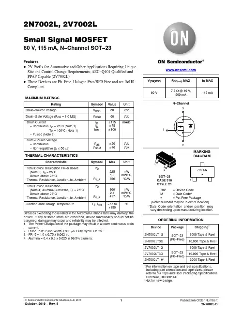

2N7002KTrenchMOS™ logic level FETRev. 01 — 20 October 2003Product dataM3D0881.Product profile1.1DescriptionN-channel enhancement mode field-effect transistor in a plastic package using TrenchMOS™ technology.1.2Features1.3Applications1.4Quick reference data2.Pinning informations Logic level compatible s Very fast switchings Subminiature surface mount package s Gate-source ESD protection diodes.s Relay drivers High speed line driver.s V DS ≤60V s I D ≤340mA s P tot ≤0.83Ws R DSon ≤3.9Ω.Table 1:Pinning - SOT23, simplified outline and symbolPin Description Simplified outlineSymbol1gate (g)SOT232source (s)3drain (d)MSB003Top view123gds03ab603.Ordering informationTable 2:Ordering informationType number PackageName Description Version2N7002K SOT23Plastic surface mounted package; 3 leads.SOT23 4.Limiting valuesTable 3:Limiting valuesIn accordance with the Absolute Maximum Rating System (IEC 60134).Symbol Parameter Conditions Min Max Unit V DS drain-source voltage (DC)25°C≤T j≤150°C-60VV DGR drain-gate voltage (DC)25°C≤T j≤150°C; R GS=20kΩ-60VV GS gate-source voltage (DC)-±15VI D drain current (DC)T sp=25°C; V GS=10V;Figure2and3-340mAT sp=100°C; V GS=10V;Figure2-215mA I DM peak drain current T sp=25°C; pulsed; t p≤10µs;Figure3-680mA P tot total power dissipation T sp=25°C;Figure1-0.83W T stg storage temperature−65+150°C T j junction temperature−65+150°C Source-drain diodeI S source (diode forward) current (DC)T sp=25°C-340mA I SM peak source (diode forward) current T sp=25°C; pulsed; t p≤10µs-680mA Electrostatic discharge voltageV esd electrostatic discharge voltage Human Body Model1; C=100pF; R=1.5kΩ-1kVFig 1.Normalized total power dissipation as afunction of solder point temperature.Fig 2.Normalized continuous drain current as afunction of solder point temperature.T sp =25°C; I DM is single pulse; V GS =10VFig 3.Safe operating area; continuous and peak drain currents as a function of drain-source voltage.03aa1704080120050100150200(%)T sp (°C)P der 03aa2504080120050100150200T sp (°C)I der (%)P der P totP tot 25C °()-----------------------100%×=I der I DI D 25C °()-------------------100%×=03an6610-210-11110102V DS (V)I D (A)DC100 ms10 msLimit R DSon = V DS / I D1 mst p = 10 µs100 µs5.Thermal characteristics5.1Transient thermal impedanceTable 4:Thermal characteristicsSymbol ParameterConditionsMin Typ Max Unit R th(j-sp)thermal resistance from junction to solder point Figure 4--150K/W R th(j-a)thermal resistance from junction to ambientminimum footprint;mounted on a printed-circuit board-350-K/WFig 4.Transient thermal impedance from junction to solder point as a function of pulse duration.03aa3911010210310-510-410-310-210-1110t p (s)Z th(j-sp)(K/W)single pulseδ = 0.50.20.10.050.02t pt p TPtTδ =6.CharacteristicsTable 5:CharacteristicsT j=25°C unless otherwise specified.Symbol Parameter Conditions Min Typ Max Unit Static characteristicsV(BR)DSS drain-source breakdown voltage I D=10µA; V GS=0VT j=25°C6075-VT j=−55°C55--VV(BR)GSS drain-source breakdown voltage I G=±1mA; V DS=0V1622-VV GS(th)gate-source threshold voltage I D=1mA; V DS=V GS;Figure9VT j=25°C12-VT j=150°C0.6--VT j=−55°C-- 3.5VI DSS drain-source leakage current V DS=48V; V GS=0VT j=25°C-0.011µAT j=150°C--10µA I GSS gate-source leakage current V GS=±10V; V DS=0V-50500nA R DSon drain-source on-state resistance V GS=10V; I D=500mA;Figure7and8T j=25°C- 2.8 3.9ΩT j=150°C- 5.27.2ΩV GS=4.5V; I D=200mA;Figure7and8- 3.8 5.3ΩDynamic characteristicsC iss input capacitance V GS=0V; V DS=10V; f=1MHz;Figure11-1340pFC oss output capacitance-830pF C rss reverse transfer capacitance-410pFt on turn-on time V DD=50V; R L=250Ω;V GS=10V;R G=50Ω; R GS=50Ω-310nst off turn-off time-915ns Source-drain diodeV SD source-drain (diode forward) voltage I S=300mA; V GS=0V;Figure12-0.93 1.5Vt rr reverse recovery time I S=300mA; dI S/dt=−100A/µs;V GS=0V; V R=25V -30-nsQ r recovered charge-30-nCT j =25°C T j =25°C and 150°C; V DS >I D x R DSonFig 5.Output characteristics: drain current as afunction of drain-source voltage;typical values.Fig 6.Transfer characteristics: drain current as afunction of gate-source voltage; typical values.T j =25°CFig 7.Drain-source on-state resistance as a functionof drain current; typical values.Fig 8.Normalized drain-source on-state resistance factor as a function of junction temperature.03an7000.10.20.30.40.500.511.52V DS (V)I D (A) 3.5 VT j = 25 °CV GS = 10V4 V4.5 V3 V6 V03an7200.10.20.30.40.50246V GS (V)I D (A)V DS > I D x R DSonT j = 25 °C150 °C03an71024681000.10.20.30.40.5I D (A)R DSon (Ω)V GS = 3.5 VT j = 25 °C4.5 V4 V10 V6 V 03aa2800.61.21.82.4-6060120180a T j (°C)a RDSon R DSon 25C °()----------------------------=I D =1mA; V DS =V GS T j =25°C; V DS =5VFig 9.Gate-source threshold voltage as a function ofjunction temperature.Fig 10.Sub-threshold drain current as a function ofgate-source voltage.V GS =0V; f =1MHzFig 11.Input, output and reverse transfer capacitances as a function of drain-source voltage; typical values.03aa3400.61.21.82.4-6060120180T j (°C)V GS(th)(V)typmin03aa3710-610-510-410-310-210-100.61.21.82.4V GS (V)I D (A)typmin03aa4611010210-11 10102V DS (V)C (pF)C issC ossC rssT j =25°C and 150°C; V GS =0V I D =0.5A; V DD =48VFig 12.Source (diode forward) current as a function ofsource-drain (diode forward) voltage; typical values.Fig 13.Gate-source voltage as a function of gatecharge; typical values.03an7300.10.20.30.40.500.30.60.91.2V SD (V)I S (A)T j = 25 °C150 °CV GS = 0 V03ab090510150.30.60.91.2Q G (nC)V GS (V)I D = 0.5AV DD = 48 V T j = 25 °C7.Package outlineFig 14.SOT23.UNIT A 1max.b p c D E e 1H E L p Q w v REFERENCESOUTLINE VERSION EUROPEAN PROJECTIONISSUE DATE 97-02-2899-09-13IECJEDEC EIAJmm0.10.480.380.150.093.02.81.41.20.95e 1.92.52.10.550.450.10.2DIMENSIONS (mm are the original dimensions)0.450.15SOT23TO-236ABb pD e 1eAA 1L pQdetail XH EE w M v M ABAB 01 2 mmscaleA 1.10.9cX123Plastic surface mounted package; 3 leadsSOT238.Revision historyTable 6:Revision historyRev Date CPCN Description0120031020Product data (9397 750 11703)分销商库存信息: NXP2N7002K,215。
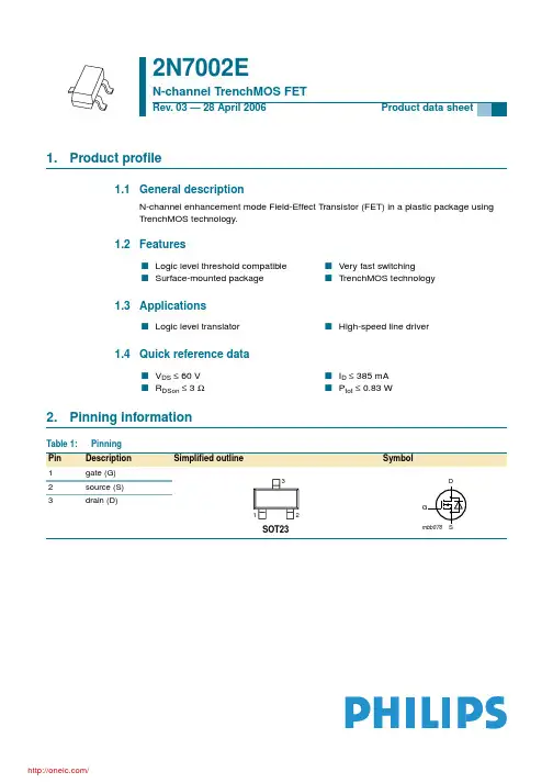
1.Product profile1.1General descriptionN-channel enhancement mode Field-Effect Transistor (FET) in a plastic package using TrenchMOS technology.1.2Features1.3Applications1.4Quick reference data2.Pinning information2N7002EN-channel TrenchMOS FETRev. 03 — 28 April 2006Product data sheets Logic level threshold compatible s Very fast switchings Surface-mounted packages TrenchMOS technologys Logic level translators High-speed line drivers V DS ≤60V s I D ≤385mA s R DSon ≤3Ωs P tot ≤0.83WTable 1:Pinning Pin Description Simplified outline Symbol1gate (G)SOT232source (S)3drain (D)123SDGmbb0763.Ordering informationTable 2:Ordering informationType number PackageName Description Version2N7002E TO-236AB plastic surface-mounted package; 3 leads SOT23 4.Limiting valuesTable 3:Limiting valuesIn accordance with the Absolute Maximum Rating System (IEC 60134).Symbol Parameter Conditions Min Max Unit V DS drain-source voltage25°C≤T j≤150°C-60VV DGR drain-gate voltage (DC)25°C≤T j≤150°C; R GS=20kΩ-60VV GS gate-source voltage-±30VV GSM peak gate-source voltage t p≤50µs; pulsed; duty cycle=25%-±40VI D drain current T sp=25°C; V GS=10V; see Figure2and3-385mAT sp=100°C; V GS=10V; see Figure2-245mA I DM peak drain current T sp=25°C; pulsed; t p≤10µs; see Figure3- 1.5AP tot total power dissipation T sp=25°C; see Figure1-0.83W T stg storage temperature−65+150°C T j junction temperature−65+150°C Source-drain diodeI S source current T sp=25°C-385mA I SM peak source current T sp=25°C; pulsed; t p≤10µs- 1.5mAFig 1.Normalized total power dissipation as afunction of solder point temperatureFig 2.Normalized continuous drain current as afunction of solder point temperatureT sp =25°C; I DM is single pulseFig 3.Safe operating area; continuous and peak drain currents as a function of drain-source voltage03aa174080120050100150200T sp (°C)P der (%)03aa254080120050100150200T sp (°C)I der (%)P der P totP tot 25C °()------------------------100%×=I der I DI D 25C °()--------------------100%×=03ai1010-210-1110 110102V DS (V)I D (A)DC1 ms 100 µsLimit R DSon = V DS / I D10 ms 100 ms10 µst p =5.Thermal characteristics[1]Mounted on a printed-circuit board; minimum footprint; vertical in still airTable 4:Thermal characteristicsSymbol ParameterConditions Min Typ Max Unit R th(j-sp)thermal resistance from junction to solder point see Figure 4--150K/W R th(j-a)thermal resistance from junction to ambient[1]--350K/WFig 4.Transient thermal impedance from junction to solder point as a function of pulse duration003aab35811010210310-510-410-310-210-1110t p (s)Z th(j-sp) (K/W)single pulse0.20.10.05δ = 0.50.026.CharacteristicsTable 5:CharacteristicsT j=25°C unless otherwise specified.Symbol Parameter Conditions Min Typ Max Unit Static characteristicsV(BR)DSS drain-source breakdownvoltage I D=10µA; V GS=0VT j=25°C60--V T j=−55°C55--VV GS(th)gate-source threshold voltage I D=0.25mA;V DS=V GS;see Figure9and10T j=25°C12 2.5VT j=150°C0.6--VT j=−55°C-- 2.75V I DSS drain leakage current V DS=48V; V GS=0VT j=25°C--1µAT j=150°C--10µA I GSS gate leakage current V GS=±15V; V DS=0V-10100nAR DSon drain-source on-stateresistance V GS=10V; I D=500mA; see Figure6and8T j=25°C-0.783ΩT j=150°C- 1.45 5.5ΩV GS=4.5V; I D=75mA; see Figure6and8- 1.24ΩDynamic characteristicsQ G(tot)total gate charge I D=300mA; V DS=30V; V GS=10V;see Figure11and12-0.69-nCQ GS gate-source charge-0.1-nC Q GD gate-drain charge-0.27-nCC iss input capacitance V GS=0V; V DS=10V; f=1MHz;see Figure14-3150pFC oss output capacitance- 6.830pF C rss reverse transfer capacitance- 3.510pFt on turn-on time V DS=50V; R L=250Ω; V GS=10V;R G=50Ω; R GS=50Ω- 2.510nst off turn-off time-1115ns Source-drain diodeV SD source-drain voltage I S=300mA; V GS=0V; see Figure13-0.85 1.5V t rr reverse recovery time I S=300mA; dI S/dt=−100A/µs; V GS=0V-30-ns Q r recovered charge-30-nCT j =25°C T j =25°CFig 5.Output characteristics: drain current as afunction of drain-source voltage; typical valuesFig 6.Drain-source on-state resistance as a functionof drain current; typical valuesT j =25°C and 150°C; V DS >I D ×R DSonFig 7.Transfer characteristics: drain current as afunction of gate-source voltage; typical valuesFig 8.Normalized drain-source on-state resistancefactor as a function of junction temperature03ai120.20.40.60.8100.51 1.52V DS (V)I D (A)1054.543.5V GS (V) =03ai141000200030004000500000.20.40.60.81I D (A)R DSon (m Ω)454.510V GS (V) =03ai160.20.40.60.810246V GS (V)I D (A)T j = 150 °C25 °C03aa2800.61.21.82.4-60060120180T j (°C)a a R DSonR DSon 25C °()------------------------------=I D =0.25mA; V DS =V GS T j =25°C; V DS =5VFig 9.Gate-source threshold voltage as a function ofjunction temperatureFig 10.Sub-threshold drain current as a function ofgate-source voltageI D =0.3A; V DS =30VFig 11.Gate-source voltage as a function of gatecharge; typical valuesFig 12.Gate charge waveform definitions003aab1010123-60060120180T j (°C)V GS(th)(V)mintypmax003aab10010-610-510-410-30123V GS (V)I D (A)min typ max003aab35924681000.20.40.60.8Q G (nC)V GS (V)I D = 0.3 A T j = 25 °C V DS = 30 V003aaa508V GSV GS(th)Q GS1Q GS2Q GDV DSQ G(tot)I DQ GSV GS(pl)T j =25°C and 150°C; V GS =0V V GS =0V; f =1MHzFig 13.Source current as a function of source-drainvoltage; typical valuesFig 14.Input,output and reverse transfer capacitancesas a function of drain-source voltage; typical values03ai1700.20.40.60.810.20.40.60.81V SD (V)I S (A)T j = 25 °C150 °C03ai1811010210-11 10102V DS (V)C (pF)C issC rssC oss7.Package outlineFig 15.Package outline SOT23UNIT A 1max.b p c D E e 1H E L p Q w v REFERENCESOUTLINE VERSION EUROPEAN PROJECTIONISSUE DATE 04-11-0406-03-16IECJEDEC JEITAmm0.10.480.380.150.093.02.81.41.20.95e 1.92.52.10.550.450.10.2DIMENSIONS (mm are the original dimensions)0.450.15SOT23TO-236ABb pD e 1eAA 1L pQdetail XH EE w M v M ABAB 01 2 mmscaleA 1.10.9cX123Plastic surface-mounted package; 3 leadsSOT238.Revision historyTable 6:Revision historyDocument ID Release date Data sheet status Change notice Doc. number Supersedes 2N7002E_320060428Product data sheet--2N7002E_2 Modifications:•Table 5 “Characteristics”: V GS(th) I D condition modified•Table 5 “Characteristics”: V GS(th) maximum limits modified•Table 5 “Characteristics”: R DSon typical values modified•Table 5 “Characteristics”: g fs removed•Table 5 “Characteristics”: Addition of Q G(tot), Q GS and Q GD•Table 5 “Characteristics”: C iss, C oss and C rss values modified•Table 5 “Characteristics”: t on and t off typical values modified•Figure3,4,5,6,7,9,10,13 and14: modified•Figure11: added2N7002E_220050426Product data sheet-9397 750 149442N7002E-01 2N7002E-0120020211Product data-9397 750 09095-分销商库存信息: NXP2N7002E,215。
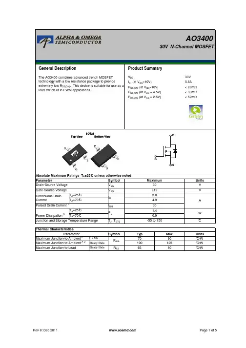

2N7002ESmall Signal MOSFET60 V, 310 mA, Single, N−Channel, SOT−23Features•Low R DS(on)•Small Footprint Surface Mount Package•Trench Technology•This is a Pb−Free DeviceApplications•Low Side Load Switch•Level Shift Circuits•DC−DC Converter•Portable Applications i.e. DSC, PDA, Cell Phone, etc.MAXIMUM RATINGS (T J = 25°C unless otherwise stated)Rating Symbol Value Unit Drain−to−Source Voltage V DSS60V Gate−to−Source Voltage V GS±20VDrain Current (Note 1)Steady State T A = 25°CT A = 85°Ct < 5 s T A = 25°CT A = 85°C I D260190310220mAPower Dissipation (Note 1) Steady Statet < 5 s P D300420mWPulsed Drain Current (t p = 10 m s)IDM 1.2AOperating Junction and Storage Temperature Range T J, T STG−55 to+150°CSource Current (Body Diode)I S300mALead Temperature for Soldering Purposes (1/8″ from case for 10 s)T L260°CStresses exceeding Maximum Ratings may damage the device. Maximum Ratings are stress ratings only. Functional operation above the Recommended Operating Conditions is not implied. Extended exposure to stresses above the Recommended Operating Conditions may affect device reliability. THERMAL CHARACTERISTICSCharacteristic Symbol Max Unit Junction−to−Ambient − Steady State(Note1)R q JA417°C/W Junction−to−Ambient − t ≤ 5 s (Note 1)R q JA3001.Surface−mounted on FR4 board using 1 in sq pad size (Cu area = 1.127 insq [1 oz] including traces)Device Package Shipping†ORDERING INFORMATION2N7002ET1G3000/Tape & ReelSOT−23(Pb−Free)†For information on tape and reel specifications, including part orientation and tape sizes, please refer to our T ape and Reel Packaging Specifications Brochure, BRD8011/D.ELECTRICAL CHARACTERISTICS (T J = 25°C unless otherwise specified)Parameter Symbol Test Condition Min Typ Max Units OFF CHARACTERISTICSDrain−to−Source Breakdown Voltage V(BR)DSS V GS = 0 V, I D = 250 m A60V Drain−to−Source Breakdown VoltageTemperature CoefficientV(BR)DSS/T J75mV/°CZero Gate Voltage Drain Current I DSS VGS = 0 V,V DS = 60 V T J = 25°C1m A T J = 125°C500Gate−to−Source Leakage Current I GSS V DS = 0 V, V GS = ±20 V±100nA ON CHARACTERISTICS (Note 2)Gate Threshold Voltage V GS(TH)V GS = V DS, I D = 250 m A 1.0 2.5V Negative Threshold TemperatureCoefficientV GS(TH)/T J 4.4mV/°C Drain−to−Source On Resistance R DS(on)V GS = 10 V, I D = 240 mA0.86 2.5WV GS = 4.5 V, I D = 50 mA 1.1 3.0Forward Transconductance g FS V DS = 5 V, I D = 200 mA80S CHARGES AND CAPACITANCESInput Capacitance C ISSV GS = 0 V, f = 1 MHz,V DS = 25 V 26.7pFOutput Capacitance C OSS 4.6 Reverse Transfer Capacitance C RSS 2.9Total Gate Charge Q G(TOT)V GS = 5 V, V DS = 10 V;I D = 240 mA 0.81nCThreshold Gate Charge Q G(TH)0.31 Gate−to−Source Charge Q GS0.48 Gate−to−Drain Charge Q GD0.08 SWITCHING CHARACTERISTICS, V GS = V (Note 3)Turn−On Delay Time t d(ON)V GS = 10 V, V DD = 30 V,I D = 200 mA, R G = 10 W 1.7nsRise Time t r 1.2 Turn−Off Delay Time t d(OFF) 4.8 Fall Time t f 3.6 DRAIN−SOURCE DIODE CHARACTERISTICSForward Diode Voltage V SD VGS = 0 V,I S = 200 mA T J = 25°C0.79 1.2V T J = 85°C0.72.Pulse Test: pulse width ≤ 300 m s, duty cycle ≤ 2%3.Switching characteristics are independent of operating junction temperaturesFigure 5. On −Resistance vs. Gate −to −SourceVoltage Figure 6. On −Resistance Variation withTemperatureV GS , GATE −TO −SOURCE VOLTAGE (V)T J , JUNCTION TEMPERATURE (°C)I D , D R A I N C U R R E N T (A )R D S (o n ), D R A I N −T O −S O U R C E R E S I S T A N C E (W )R D S (o n ), D R A I N −T O −S O U R C E R E S I S T A N C E (W )Figure 9. Diode Forward Voltage vs. CurrentV SD , SOURCE −TO −DRAIN VOLTAGE (V)10203040C , C A P A C I T A N C E (p F )PACKAGE DIMENSIONSSOT −23 (TO −236)CASE 318−08ISSUE AHSTYLE 21:PIN 1.GATE2.SOURCE3.DRAINV NOTES:*For additional information on our Pb −Free strategy and soldering details, please download the ON Semiconductor Soldering and Mounting Techniques Reference Manual, SOLDERRM/D.SOLDERING FOOTPRINT*ON Semiconductor and are registered trademarks of Semiconductor Components Industries, LLC (SCILLC). SCILLC reserves the right to make changes without further notice to any products herein. SCILLC makes no warranty, representation or guarantee regarding the suitability of its products for any particular purpose, nor does SCILLC assume any liability arising out of the application or use of any product or circuit, and specifically disclaims any and all liability, including without limitation special, consequential or incidental damages.“Typical” parameters which may be provided in SCILLC data sheets and/or specifications can and do vary in different applications and actual performance may vary over time. All operating parameters, including “Typicals” must be validated for each customer application by customer’s technical experts. SCILLC does not convey any license under its patent rights nor the rights of others. SCILLC products are not designed, intended, or authorized for use as components in systems intended for surgical implant into the body, or other applications intended to support or sustain life, or for any other application in which the failure of the SCILLC product could create a situation where personal injury or death may occur. Should Buyer purchase or use SCILLC products for any such unintended or unauthorized application, Buyer shall indemnify and hold SCILLC and its officers, employees, subsidiaries, affiliates,and distributors harmless against all claims, costs, damages, and expenses, and reasonable attorney fees arising out of, directly or indirectly, any claim of personal injury or death associated with such unintended or unauthorized use, even if such claim alleges that SCILLC was negligent regarding the design or manufacture of the part. SCILLC is an Equal Opportunity/Affirmative Action Employer. This literature is subject to all applicable copyright laws and is not for resale in any manner.PUBLICATION ORDERING INFORMATION。