电磁炉芯片
- 格式:doc
- 大小:27.50 KB
- 文档页数:14

电磁炉芯片电磁炉芯片是指能够实现电磁炉基本功能的核心部件。
它通过控制功率电子器件的开启与关闭,来实现电磁炉的加热、温度控制和保护等功能。
电磁炉芯片作为电磁炉的“大脑”,对整个电磁炉的效率、安全性和使用寿命起到非常重要的作用。
首先,电磁炉芯片负责控制功率电子器件的开关。
电磁炉使用的是交流电,而电磁炉芯片通过对交流电进行适当的调整,将其转换为适合电磁炉使用的直流电。
这样可以确保功率电子器件能够正常工作,并且提高电磁炉的效率。
同时,电磁炉芯片还能够控制功率电子器件的开启与关闭时间,从而精确控制电磁炉的加热功率,使得食物可以均匀、快速地受热。
其次,电磁炉芯片还负责控制电磁炉的温度。
电磁炉芯片通过传感器感知电磁炉和食物的温度,再根据用户设定的温度,通过对功率电子器件的控制,实现对电磁炉的温度调节。
这样,无论是煮开水还是烹饪美食,都可以根据需要进行温度调节,保证食物的烹饪效果。
此外,电磁炉芯片还拥有丰富的保护功能。
电磁炉芯片可以监测功率电子器件和传感器的工作状态,一旦发现故障,如过载、短路或温度异常,电磁炉芯片会立即切断电源,以保护电磁炉和用户的安全。
此外,电磁炉芯片还有过热保护功能,当温度超过设定的安全范围时,电磁炉芯片会自动降低功率或关闭电源,以防止电磁炉的过热。
电磁炉芯片还具备通信功能,通过与电磁炉控制面板的互联,可以实现对电磁炉的参数设置和菜谱选择等功能。
电磁炉芯片还可以进行远程控制,通过手机等设备远程控制电磁炉的开关、温度和功率等参数,提供了更加便捷的使用体验。
总的来说,电磁炉芯片通过控制功率电子器件的开关、温度调节和保护功能,实现了电磁炉的基本功能。
它能够提高电磁炉的加热效率,保证食物的烹饪效果,同时还能保护电磁炉和用户的安全。
随着科技的进步,电磁炉芯片的功能也在不断提升,为用户带来更加便捷、安全、智能的使用体验。
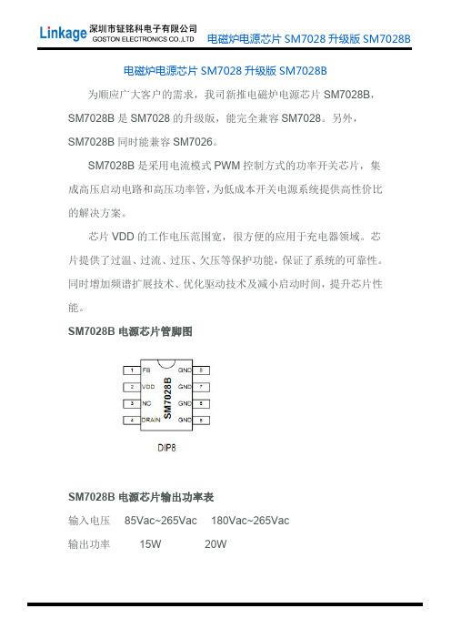
电磁炉电源芯片SM7028升级版SM7028B
为顺应广大客户的需求,我司新推电磁炉电源芯片SM7028B,SM7028B是SM7028的升级版,能完全兼容SM7028。
另外,
SM7028B同时能兼容SM7026。
SM7028B是采用电流模式PWM控制方式的功率开关芯片,集成高压启动电路和高压功率管,为低成本开关电源系统提供高性价比的解决方案。
芯片VDD的工作电压范围宽,很方便的应用于充电器领域。
芯片提供了过温、过流、过压、欠压等保护功能,保证了系统的可靠性。
同时增加频谱扩展技术、优化驱动技术及减小启动时间,提升芯片性能。
SM7028B电源芯片管脚图
SM7028B电源芯片输出功率表
输入电压85Vac~265Vac180Vac~265Vac
输出功率15W20W
注:输出功率10W以上,建议根据实际方案增加散热措施:
1.5678脚增加PCB散热;
2.增加独立散热片;
3.其他散热措施。
典型示意电路图
SM7028B特点:
1.85Vac~265Vac宽电压输入
2.9V~30V宽VDD工作电压范围
3.60KHz固定开关频率
4.待机功耗小于120mW@220Vac
5.集成高压启动电路
6.集成高压功率开关
7.电流模式PWM控制方式
8.开机软启动功能
9.内置频谱扩展技术,改善EMC性能
10.内置过温、过流、过压、欠压等保护功能
11.封装形式:EDIP8
SM702B广泛应用于小家电电源、小功率充电器、适配器、待机电源、DVD/DVB以及其他便携式设备电源等领域。
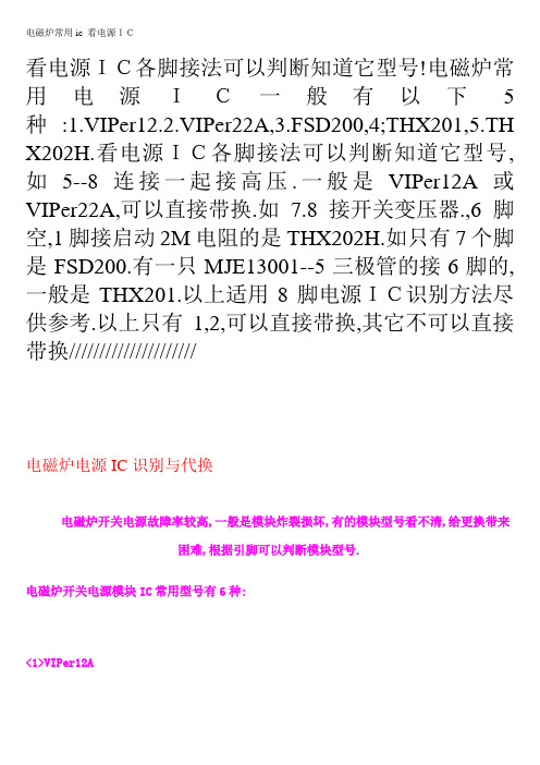
电磁炉常用ic 看电源IC看电源IC各脚接法可以判断知道它型号!电磁炉常用电源IC一般有以下5种:1.VIPer12.2.VIPer22A,3.FSD200,4;THX201,5.TH X202H.看电源IC各脚接法可以判断知道它型号,如5--8连接一起接高压.一般是VIPer12A或VIPer22A,可以直接带换.如7.8接开关变压器.,6脚空,1脚接启动2M电阻的是THX202H.如只有7个脚是FSD200.有一只MJE13001--5三极管的接6脚的,一般是THX201.以上适用8脚电源IC识别方法尽供参考.以上只有1,2,可以直接带换,其它不可以直接带换/////////////////////电磁炉电源IC识别与代换电磁炉开关电源故障率较高,一般是模块炸裂损坏,有的模块型号看不清,给更换带来困难,根据引脚可以判断模块型号.电磁炉开关电源模块IC常用型号有6种:<1>VIPer12A<2>VIPer22A<3>THX201A<4>THX202H<5>FSD200<6>LNK364P如引脚5,6,7.8.接300V高压.1.2.脚接地.一般是:VIPer12A或VIPer22A<1><2>.两者可以直接带换.如引脚7脚接三极管MJE13007的基极,6脚接三极管的发射极,4.脚接地.2脚空,是:THX201A.如:只有7只脚.8脚接高压.7.脚接开关变压器.1.2.3.脚接地.无6脚.4.脚接三极管集电极.是:FSD200.如1脚接启动电阻.7.8.脚接开关变压器.3脚接地.6.脚空.是:THX202H.如1.2.7.8.脚接地.5脚接开关变压器,无6脚是LNK364P.供维修参考FSD200 电磁炉常用电源IC。

电磁炉电源芯片12a3脚对地电阻值文档下载说明Download tips: This document is carefully compiled by this editor. I hope that after you download it, it can help you solve practical problems. The document 电磁炉电源芯片12a3脚对地电阻值can be customized and modified after downloading, please adjust and use it according to actual needs, thank you! In addition, this shop provides you with various types of practical materials, such as educational essays, diary appreciation, sentence excerpts, ancient poems, classic articles, topic composition, work summary, word parsing, copy excerpts, other materials and so on, want to knowdifferent data formats and writing methods, please pay attention!电磁炉电源芯片是电磁炉的核心部件之一,其功能主要是对电源进行管理和控制,以确保电磁炉正常运行。
而电源芯片的12A3脚对地电阻值则是电磁炉电路中一个重要的参数,它直接影响到电磁炉的工作效率和安全性。
12A3脚对地电阻值是指电源芯片的第12脚到地之间的电阻数值。
这个数值一般是测量电源芯片的接地电阻,用来判断电源芯片是否正常工作。

电磁炉常用开关电源芯片介绍电磁炉虽然品牌厂家众多,但其内部构成原理都大同小异,今天我来给大家扒一扒电磁炉中常用的几种开关电源管理芯片,希望对从事此方面维修的师傅有所帮助。
•VIPER12AVPIER 12A是采用电流模式PWM控制方式的功率开关芯片,集成高压启动电路和高压功率管,为低成本开关电源系统提供高性价比的解决方案。
芯片VDD的工作电压范围宽,很方便的应用于充龟器领域。
另外还提供了过温、过流、过压等保护功能,保证了解系统的可靠性。
管脚示意图如下。
其中4脚VDD为芯片电源供电端,1、2脚为芯片内部MOS管的源极,同时也是芯片地。
3脚FB为反馈输入端,5678脚为芯片的启动端,同时作为内部MOS管的漏极。
维修时,可以用VIPER22A替换使用。
•THX203HTHX203H为高效能电流模式PWM控制器。
专为高性价比AC/DC转换器设计。
在85V-265V的宽电压范围内提供高达12W的连续输出功率,峰值输出功率更可以达到18W。
该电源控制器可工作于典型的反激电路拓扑中,构成简洁的AD/DC转换器。
其管脚示意图如下其中2脚和3脚为别为芯片供电端和接地端。
1脚OB为启动电流输入端,外接启动电阻。
4脚CT为振荡电容端,外接定时电容。
5脚FB为反馈端。
6脚IS为开关电流取样端口,外接取样电阻。
7脚和8脚为输出端,接开关变压器。
FSD200该芯片为双列直插7脚封装,内含700V耐压 SenseFET功率开关管。
工作电压230VAC,±15%时,输出功率5W;工作电压85-265VAC时,输出功率4W。
最高开关频率134kHz。
该控制芯片由一个耐压700V 的功率MOSFET 开关管和电源控制器两部分组成。
其控制方式不同于传统的PWM 型开关电源,采用简单的开/关控制输出电压,其瞬态响应时间比传统的PWM型要快,而且具有线电压欠压保护功能。
管脚图见下图。
其5脚VCC为供电脚,123脚GND为接地端,4脚VFB为电压反馈引脚,7脚DRAIN为内部MOS管的漏极,8脚VSTR为启动引脚。

电磁炉的晶板有什么作用电磁炉是一种利用电磁感应原理加热的厨房电器,它的工作原理是利用电磁感应加热锅具底部,从而实现加热食物的目的。
而电磁炉的晶板则是电磁炉的关键部件之一,它具有多种重要的作用,下面我们就来详细了解一下电磁炉的晶板有什么作用。
1. 传热效果好。
电磁炉的晶板是由特殊的材料制成的,可以有效地将电磁感应产生的热量传导到锅具底部,从而实现快速加热食物的目的。
晶板的材料通常是铁、铝等具有良好导热性能的金属材料,因此可以有效地提高电磁炉的传热效果,节约能源的同时也能够快速烹饪食物。
2. 温度控制精准。
电磁炉的晶板可以根据用户的设定精准地控制加热温度,从而实现更加精细化的烹饪操作。
晶板内部集成了先进的温控技术,可以实时监测锅具底部的温度并进行调节,确保食物的加热温度恰到好处,避免过热或者过冷的情况发生,保证食物的口感和营养。
3. 节能环保。
电磁炉的晶板在加热食物的过程中可以减少能量的浪费,因为它可以直接将热量传导到锅具底部,而不会像传统的燃气灶一样产生大量的热量散失。
此外,晶板还可以根据锅具的大小自动调节加热面积,避免能量的浪费,从而实现节能环保的效果。
4. 安全可靠。
晶板的材料通常是不易燃烧的金属材料,因此具有较高的耐高温性能和抗氧化性能,可以确保在高温环境下不会产生有害气体。
此外,晶板内部还集成了多种安全保护装置,可以在发生异常情况时及时切断电源,保障用户和设备的安全。
5. 易于清洁。
晶板的表面通常采用特殊的防污涂层处理,可以有效地防止食物残渣和油渍的附着,从而使清洁工作更加轻松。
用户只需用湿布擦拭晶板表面即可轻松清除污垢,不需要使用任何化学清洁剂,既方便又环保。
总的来说,电磁炉的晶板作为电磁炉的重要组成部分,具有传热效果好、温度控制精准、节能环保、安全可靠、易于清洁等多种重要作用。
它不仅可以提高电磁炉的加热效率,还可以保障用户和设备的安全,是电磁炉不可或缺的关键部件。
随着科技的不断进步,相信电磁炉的晶板会在未来发展出更多更加先进的功能,为用户带来更加便捷、高效的烹饪体验。
电磁炉电源芯片有几种电磁炉电源芯片主要有以下几种类型:1. PWM调制器芯片:PWM调制器芯片是一种常见的电磁炉电源芯片,它能够广泛应用于电磁炉的功率控制。
这种芯片通过改变脉冲宽度调制(PWM)的方式来改变电磁炉的输出功率,从而实现对电磁炉的温度控制。
PWM调制器芯片具有高效率、精确控制和稳定性强等特点,被广泛应用于电磁炉的控制系统中。
2. 开关电源芯片:开关电源芯片是电磁炉电源芯片中重要的一种类型。
开关电源芯片能够将输入电源的交流电转换成恒定的直流电,并提供给电磁炉的各个部件。
开关电源芯片具有高效率、小型化、稳定性好、输出电流能力强等优点,在电磁炉中的应用十分广泛。
3. 锁相环芯片:锁相环芯片是一种用于在电磁炉中生成定频脉冲的电源芯片。
锁相环芯片通过接收和分析外部频率信号,并根据设定的频率输出脉冲信号,从而控制电磁炉的工作频率。
锁相环芯片具有快速响应、频率稳定等特点,被广泛用于电磁炉的频率控制部分。
4. 驱动芯片:驱动芯片是电磁炉中用来驱动电源开关管的芯片。
它通过控制电源开关管的导通和断开,来实现对电源的开关控制,从而控制电磁炉的工作状态。
驱动芯片具有输出电流能力强、响应速度快等特点,被广泛应用于电磁炉的控制系统中。
5. 控制芯片:控制芯片是电磁炉电源芯片的核心部分,它负责电磁炉整个控制系统的功能实现。
控制芯片可以集成多种功能,如温度监测、自动控制、故障检测等。
这种芯片可以根据不同的需求和规格进行选择和设计,具有较高的灵活性和可定制性。
以上是电磁炉电源芯片的主要类型,它们在电磁炉的功率调节、工作频率控制、输出电流驱动等方面发挥着重要的作用。
不同类型的芯片可根据电磁炉的需求进行选择和组合使用,以实现电磁炉的稳定运行和高效工作。
LM139/LM239/LM339/LM2901/LM3302Low Power Low Offset Voltage Quad ComparatorsGeneral DescriptionThe LM139series consists of four independent precision voltage comparators with an offset voltage specification as low as 2mV max for all four comparators.These were de-signed specifically to operate from a single power supply over a wide range of voltages.Operation from split power supplies is also possible and the low power supply current drain is independent of the magnitude of the power supply voltage.These comparators also have a unique characteris-tic in that the input common-mode voltage range includes ground,even though operated from a single power supply voltage.Application areas include limit comparators,simple analog to digital converters;pulse,squarewave and time delay gen-erators;wide range VCO;MOS clock timers;multivibrators and high voltage digital logic gates.The LM139series was designed to directly interface with TTL and CMOS.When op-erated from both plus and minus power supplies,they will di-rectly interface with MOS logic —where the low power drain of the LM339is a distinct advantage over standard compara-tors.Advantagesn High precision comparatorsn Reduced V OS drift over temperature n Eliminates need for dual supplies n Allows sensing near GNDn Compatible with all forms of logicnPower drain suitable for battery operationFeaturesn Wide supply voltage range—LM139/139A Series 2to 36V DC or ±1to ±18V DC —LM2901:2to 36V DC or ±1to ±18V DC —LM3302:2to 28V DC or ±1to ±14V DC n Very low supply current drain (0.8mA)—independent of supply voltagen Low input biasing current:25nAn Low input offset current:±5nA n Offset voltage:±3mV n Input common-mode voltage range includes GND n Differential input voltage range equal to the power supply voltagen Low output saturation voltage:250mV at 4mA n Output voltage compatible with TTL,DTL,ECL,MOS and CMOS logic systemsConnection DiagramsDS005706-27Order Number LM139AW/883or LM139W/883(Note 1)LM139AWRQML and LM139AWRQMLV (Note 3)See NS Package Number W14BLM139AWGRQML and LM139AWGRQMLV (Note 3)See NS Package Number WG14ANovember 1999LM139/LM239/LM339/LM2901/LM3302Low Power Low Offset Voltage Quad Comparators©1999National Semiconductor Corporation Connection Diagrams(Continued)Note 1:Available per JM38510/11201Note 2:Available per SMD #5962-8873901Note 3:See STD Mil Dwg 5962R96738for Radiation Tolerant DeviceDual-In-Line PackageDS005706-2Order Number LM139J,LM139J/883(Note 1),LM139AJ,LM139AJ/883(Note 2),LM239J,LM239AJ,LM339J,LM139AJRQML and LM139AJRQMLV (Note 3)See NS Package Number J14AOrder Number LM339AM,LM339M or LM2901MSee NS Package Number M14AOrder Number LM339N,LM339AN,LM2901N or LM3302NSee NS Package Number N14AL M 139/L M 239/L M 339/L M 2901/L M 3302 2LM139/LM239/LM339/LM2901/LM3302 Absolute Maximum Ratings(Note13)If Military/Aerospace specified devices are required,please contact the National Semiconductor Sales Office/ Distributors for availability and specifications.LM139/LM239/LM339LM139A/LM239A/LM339A LM3302LM2901Supply Voltage,V+36V DC or±18V DC28V DC or±14V DC Differential Input Voltage(Note11)36V DC28V DCInput Voltage−0.3V DC to+36V DC−0.3V DC to+28V DCInput Current(V IN<−0.3V DC),(Note6)50mA50mAPower Dissipation(Note4)Molded DIP1050mW1050mWCavity DIP1190mWSmall Outline Package760mWOutput Short-Circuit to GND,(Note5)Continuous ContinuousStorage Temperature Range−65˚C to+150˚C−65˚C to+150˚CLead Temperature(Soldering,10seconds)260˚C260˚COperating Temperature Range−40˚C to+85˚CLM339/LM339A0˚C to+70˚CLM239/LM239A−25˚C to+85˚CLM2901−40˚C to+85˚CLM139/LM139A−55˚C to+125˚CSoldering InformationDual-In-Line PackageSoldering(10seconds)260˚C260˚CSmall Outline PackageVapor Phase(60seconds)215˚C215˚CInfrared(15seconds)220˚C220˚CSee AN-450“Surface Mounting Methods and Their Effect on Product Reliability”for other methods of soldering surface mount devices.ESD rating(1.5kΩin series with100pF)600V600VElectrical Characteristics(V+=5V DC,T A=25˚C,unless otherwise stated)Parameter Conditions LM139A LM239A,LM339A LM139UnitsMin Typ Max Min Typ Max Min Typ MaxInput Offset Voltage(Note12) 1.0 2.0 1.0 2.0 2.0 5.0mV DCInput Bias Current I IN(+)or I IN(−)with Output in251002525025100nA DCLinear Range,(Note8),V CM=0VInput Offset Current I IN(+)−I IN(−),V CM=0V 3.025 5.050 3.025nA DCInput Common-Mode V+=30V DC(LM3302,0V+−1.50V+−1.50V+−1.5V DCVoltage Range V+=28V DC)(Note9)Supply Current R L=∞on all Comparators,0.8 2.00.8 2.00.8 2.0mA DC R L=∞,V+=36V, 1.0 2.5 1.0 2.5mA DC(LM3302,V+=28V DC)Voltage Gain R L≥15kΩ,V+=15V DC502005020050200V/mV V o=1V DC to11V DCLarge Signal V IN=TTL Logic Swing,V REF=300300300nsResponse Time 1.4V DC,V RL=5V DC,R L=5.1kΩResponse Time V RL=5V DC,R L=5.1kΩ, 1.3 1.3 1.3µs(Note10)3Electrical Characteristics(Continued)(V +=5V DC ,T A =25˚C,unless otherwise stated)ParameterConditionsLM139A LM239A,LM339A LM139UnitsMin TypMaxMin Typ MaxMin TypMaxOutput Sink Current V IN(−)=1V DC ,V IN(+)=0, 6.016 6.016 6.016mA DC V O ≤1.5V DCSaturation Voltage V IN(−)=1V DC ,V IN(+)=0,250400250400250400mV DC I SINK ≤4mAOutput Leakage V IN(+)=1V DC ,V IN(−)=0,0.10.10.1nA DC CurrentV O =5V DCElectrical Characteristics(V +=5V DC ,T A =25˚C,unless otherwise stated)ParameterConditions LM239,LM339LM2901LM3302Units MinTyp Max Min TypMax Min TypMax Input Offset Voltage (Note 12)2.0 5.0 2.07.0320mV DC Input Bias Current I IN(+)or I IN(−)with Output in 252502525025500nA DC Linear Range,(Note 8),V CM =0V Input Offset Current I IN(+)−I IN(−),V CM =0V 5.0505503100nA DC Input Common-Mode V+=30V DC (LM3302,0V +−1.50V +−1.50V +−1.5V DC Voltage Range V+=28V DC )(Note 9)Supply CurrentR L =∞on all Comparators,0.8 2.00.8 2.00.8 2.0mA DC R L =∞,V +=36V, 1.02.51.02.51.02.5mA DC (LM3302,V+=28V DC )Voltage Gain R L ≥15k Ω,V +=15V DC 5020025100230V/mV V o =1V DC to 11V DCLarge Signal V IN =TTL Logic Swing,V REF =300300300nsResponse Time 1.4V DC ,V RL =5V DC ,R L =5.1k Ω,Response Time V RL =5V DC ,R L =5.1k Ω, 1.31.3 1.3µs (Note 10)Output Sink Current V IN(−)=1V DC ,V IN(+)=0, 6.016 6.016 6.016mA DC V O ≤1.5V DCSaturation Voltage V IN(−)=1V DC ,V IN(+)=0,250400250400250500mV DC I SINK ≤4mAOutput Leakage V IN(+)=1V DC ,V IN(−)=0,0.10.10.1nA DCCurrentV O =5V DCElectrical Characteristics(V +=5.0V DC ,(Note 7))ParameterConditionsLM139A LM239A,LM339A LM139UnitsMin TypMax Min TypMax Min TypMax Input Offset Voltage (Note 12)4.0 4.09.0mV DC Input Offset Current I IN(+)−I IN(−),V CM =0V100150100nA DC Input Bias Current I IN(+)or I IN(−)with Output in300400300nA DC Linear Range,V CM =0V (Note 8)Input Common-Mode V +=30V DC (LM3302,0V +−2.00V +−2.00V +−2.0V DC Voltage Range V +=28V DC )(Note 9)Saturation VoltageV IN(−)=1V DC ,V IN(+)=0,700700700mV DCI SINK ≤4mAL M 139/L M 239/L M 339/L M 2901/L M 33024Electrical Characteristics(Continued) (V+=5.0V DC,(Note7))Parameter ConditionsLM139A LM239A,LM339ALM139Units Min Typ Max Min Typ Max Min Typ MaxOutput Leakage Current V IN(+)=1V DC,V IN(−)=0, 1.0 1.0 1.0µA DCV O=30V DC,(LM3302,V O=28V DC)Differential Input Voltage Keep all V IN’s≥0V DC(or V−,363636V DCif used),(Note11)Electrical Characteristics(V+=5.0V DC,(Note7))Parameter Conditions LM239,LM339LM2901LM3302UnitsMin Typ Max Min Typ Max Min Typ MaxInput Offset Voltage(Note12)9.091540mV DCInput Offset Current I IN(+)−I IN(−),V CM=0V150********nA DCInput Bias Current I IN(+)or I IN(−)with Output in4002005001000nA DC Linear Range,V CM=0V(Note8)Input Common-Mode V+=30V DC(LM3302,V+=28V DC)V+−2.00V+−2.00V+−2.0V DC Voltage Range(Note9)Saturation Voltage V IN(−)=1V DC,V IN(+)=0,700400700700mV DCI SINK≤4mAOutput Leakage Current V IN(+)=1V DC,V IN(−)=0, 1.0 1.0 1.0µA DC V O=30V DC,(LM3302,V O=28V DC)Differential Input Voltage Keep all V IN’s≥0V DC(or V−,363628V DC if used),(Note11)Note4:For operating at high temperatures,the LM339/LM339A,LM2901,LM3302must be derated based on a125˚C maximum junction temperature and a thermal resistance of95˚C/W which applies for the device soldered in a printed circuit board,operating in a still air ambient.The LM239and LM139must be derated basedon a150˚C maximum junction temperature.The low bias dissipation and the“ON-OFF”characteristic of the outputs keeps the chip dissipation very small(P D≤100 mW),provided the output transistors are allowed to saturate.Note5:Short circuits from the output to V+can cause excessive heating and eventual destruction.When considering short circuits to ground,the maximum output current is approximately20mA independent of the magnitude of V+.Note6:This input current will only exist when the voltage at any of the input leads is driven negative.It is due to the collector-base junction of the input PNP tran-sistors becoming forward biased and thereby acting as input diode clamps.In addition to this diode action,there is also lateral NPN parasitic transistor action on the IC chip.This transistor action can cause the output voltages of the comparators to go to the V+voltage level(or to ground for a large overdrive)for the time duration that an input is driven negative.This is not destructive and normal output states will re-establish when the input voltage,which was negative,again returns to a value greater than−0.3V DC(at25˚)C.Note7:These specifications are limited to−55˚C≤T A≤+125˚C,for the LM139/LM139A.With the LM239/LM239A,all temperature specifications are limited to−25˚C≤T A≤+85˚C,the LM339/LM339A temperature specifications are limited to0˚C≤T A≤+70˚C,and the LM2901,LM3302temperature range is−40˚C≤T A≤+85˚C.Note8:The direction of the input current is out of the IC due to the PNP input stage.This current is essentially constant,independent of the state of the output so no loading change exists on the reference or input lines.Note9:The input common-mode voltage or either input signal voltage should not be allowed to go negative by more than0.3V.The upper end of the common-mode voltage range is V+−1.5V at25˚C,but either or both inputs can go to+30V DC without damage(25V for LM3302),independent of the magnitude of V+.Note10:The response time specified is a100mV input step with5mV overdrive.For larger overdrive signals300ns can be obtained,see typical performance char-acteristics section.Note11:Positive excursions of input voltage may exceed the power supply level.As long as the other voltage remains within the common-mode range,the com-parator will provide a proper output state.The low input voltage state must not be less than−0.3V DC(or0.3V DC below the magnitude of the negative power supply, if used)(at25˚C).Note12:At output switch point,V O≅1.4V DC,R S=0Ωwith V+from5V DC to30V DC;and over the full input common-mode range(0V DC to V+−1.5V DC),at25˚C.For LM3302,V+from5V DC to28V DC.Note13:Refer to RETS139AX for LM139A military specifications and to RETS139X for LM139military specifications.LM139/LM239/LM339/LM2901/LM33025Typical Performance CharacteristicsLM139/LM239/LM339,LM139A/LM239A/LM339A,LM3302Typical Performance CharacteristicsLM2901Supply CurrentDS005706-34Input CurrentDS005706-35Output Saturation VoltageDS005706-36Response Time for Various Input Overdrives —Negative TransitionDS005706-37Response Time for Various Input Overdrives —Positive TransitionDS005706-38Supply CurrentDS005706-39Input CurrentDS005706-40Output Saturation VoltageDS005706-41L M 139/L M 239/L M 339/L M 2901/L M 3302 6Typical Performance CharacteristicsLM2901(Continued)Application HintsThe LM139series are high gain,wide bandwidth devices which,like most comparators,can easily oscillate if the out-put lead is inadvertently allowed to capacitively couple to the inputs via stray capacitance.This shows up only during the output voltage transition intervals as the comparator changes states.Power supply bypassing is not required to solve this problem.Standard PC board layout is helpful as it reduces stray input-output coupling.Reducing this input re-sistors to <10k Ωreduces the feedback signal levels and fi-nally,adding even a small amount (1to 10mV)of positive feedback (hysteresis)causes such a rapid transition that os-cillations due to stray feedback are not possible.Simply socketing the IC and attaching resistors to the pins will cause input-output oscillations during the small transition intervals unless hysteresis is used.If the input signal is a pulse wave-form,with relatively fast rise and fall times,hysteresis is not required.All pins of any unused comparators should be tied to the negative supply.The bias network of the LM139series establishes a drain current which is independent of the magnitude of the power supply voltage over the range of from 2V DC to 30V DC .It is usually unnecessary to use a bypass capacitor across the power supply line.The differential input voltage may be larger than V +without damaging the device.Protection should be provided to pre-vent the input voltages from going negative more than −0.3V DC (at 25˚C).An input clamp diode can be used as shown in the applications section.The output of the LM139series is the uncommitted collector of a grounded-emitter NPN output transistor.Many collectors can be tied together to provide an output OR’ing function.An output pull-up resistor can be connected to any available power supply voltage within the permitted supply voltage range and there is no restriction on this voltage due to the magnitude of the voltage which is applied to the V +terminal of the LM139A package.The output can also be used as a simple SPST switch to ground (when a pull-up resistor is not used).The amount of current which the output device can sink is limited by the drive available (which is independent of V +)and the βof this device.When the maximum current limit is reached (approximately 16mA),the output transistor will come out of saturation and the output voltage will rise very rapidly.The output saturation voltage is limited by the ap-proximately 60ΩR SAT of the output transistor.The low offset voltage of the output transistor (1mV)allows the output to clamp essentially to ground level for small load currents.Typical Applications(V +=5.0V DC )Response Time for Various Input Overdrives —Negative TransitionDS005706-42Response Time for Various Input Overdrives-Positive TransitionDS005706-43Basic ComparatorDS005706-3Driving CMOSDS005706-4Driving TTLDS005706-5LM139/LM239/LM339/LM2901/LM33027Typical Applications(V +=5.0V DC )(Continued)Typical Applications(V +=15V DC )AND GateDS005706-8OR GateDS005706-9One-Shot Multivibrator 8LM139/LM239/LM339/LM2901/LM3302Typical Applications(V+=15V)(Continued)DCOne-Shot Multivibrator with Input Lock Out Array DS005706-129Typical Applications(V +=15V DC )(Continued)Large Fan-In AND GateDS005706-13ORing the OutputsDS005706-15L M 139/L M 239/L M 339/L M 2901/L M 3302 10LM139/LM239/LM339/LM2901/LM3302Typical Applications(V+=15V)(Continued)DCPulse Generator Array DS005706-1711Typical Applications(V +=15V DC )(Continued)Time Delay GeneratorDS005706-14Non-Inverting Comparator with Hysteresis DS005706-18Inverting Comparator with HysteresisDS005706-19L M 139/L M 239/L M 339/L M 2901/L M 3302 12Typical Applications(V +=15V DC )(Continued)Squarewave OscillatorDS005706-16Basic ComparatorDS005706-24Comparing Input Voltages of Opposite PolarityDS005706-20LM139/LM239/LM339/LM2901/LM330213Typical Applications(V +=15V DC )(Continued)Output StrobingDS005706-22*Or open-collector logic gate without pull-up resistorCrystal Controlled OscillatorDS005706-25L M 139/L M 239/L M 339/L M 2901/L M 3302 14Typical Applications(V +=15V DC )(Continued)T w o -D e c a d e H i g h -F r e q u e n c y V C OD S 005706-23V +=+30V D C250m V D C ≤V C ≤+50V D C700H z ≤f o ≤100k H zLM139/LM239/LM339/LM2901/LM330215Typical Applications(V +=15V DC )(Continued)Split-Supply Applications(V +=+15V DC and V −=−15V DC )Transducer AmplifierDS005706-28Zero Crossing Detector (Single Power Supply)DS005706-30MOS Clock DriverDS005706-31L M 139/L M 239/L M 339/L M 2901/L M 3302 16Split-Supply Applications(V +=+15V DC and V −=−15V DC )(Continued)Schematic DiagramZero Crossing DetectorDS005706-32Comparator With a NegativeReferenceDS005706-33DS005706-1LM139/LM239/LM339/LM2901/LM330217Physical Dimensionsinches (millimeters)unless otherwise notedCeramic Dual-In-Line Package (J)Order Number LM139J,LM139J/883,LM139AJ,LM139AJ/883,LM239J,LM239AJ,LM339JNS Package Number J14AS.O.Package (M)Order Number LM339AM,LM339M or LM2901MNS Package Number M14AL M 139/L M 239/L M 339/L M 2901/L M 3302 18Physical Dimensionsinches (millimeters)unless otherwise noted (Continued)Molded Dual-In-Line Package (N)Order Number LM339N,LM339AN,LM2901N or LM3302NNS Package Number N14AOrder Number LM139AW/883or LM139W/883NS Package Number W14BLM139/LM239/LM339/LM2901/LM330219NotesLIFE SUPPORT POLICYNATIONAL’S PRODUCTS ARE NOT AUTHORIZED FOR USE AS CRITICAL COMPONENTS IN LIFE SUPPORT DEVICES OR SYSTEMS WITHOUT THE EXPRESS WRITTEN APPROVAL OF THE PRESIDENT AND GENERAL COUNSEL OF NATIONAL SEMICONDUCTOR CORPORATION.As used herein:1.Life support devices or systems are devices or systems which,(a)are intended for surgical implant into the body,or (b)support or sustain life,and whose failure to perform when properly used in accordance with instructions for use provided in the labeling,can be reasonably expected to result in a significant injury to the user.2.A critical component is any component of a life support device or system whose failure to perform can be reasonably expected to cause the failure of the life support device or system,or to affect its safety or effectiveness.National Semiconductor Corporation AmericasTel:1-800-272-9959Fax:1-800-737-7018Email:support@National Semiconductor EuropeFax:+49(0)180-5308586Email:europe.support@Deutsch Tel:+49(0)180-5308585English Tel:+49(0)180-5327832Français Tel:+49(0)180-5329358Italiano Tel:+49(0)180-5341680National Semiconductor Asia Pacific Customer Response Group Tel:65-2544466Fax:65-2504466Email:sea.support@National Semiconductor Japan Ltd.Tel:81-3-5639-7560Fax:81-3-5639-7507L M 139/L M 239/L M 339/L M 2901/L M 3302L o w P o w e r L o w O f f s e t V o l t a g e Q u a d C o m p a r a t o r sNational does not assume any responsibility for use of any circuitry described,no circuit patent licenses are implied and National reserves the right at any time without notice to change said circuitry and specifications.。
电磁炉电源管理芯片VIPer22A测量电磁炉常用的电源芯片22A,它的型号全称是VIPer22A,这是一个常用的小功率开关电源驱动芯片,芯片集成了功率开关管,输入电压合适散热良好的情况下,其最大的输出功率可以到20W。
这个电源芯片是家用电器,比如电磁炉、饮水机等非常常用的。
VIPer22A芯片简介VIPer22A芯片基本参数VIPer22A是ST公司推出的一款小功率内置开关管的开关电源驱动芯片,欧标电压输入范围内,直插封装的最大输出功率可以到20W,贴片封装的输出功率为12W;如果是宽电压输入范围,直插封装的输出功率为12W,贴片封装的输出功率为7W。
VIPer22A的工作电压范围比较宽,为9V-38V;它的开关震荡频率固定,典型值为60kHz。
VIPer22A芯片内部结构VIPer22A芯片引脚功能排序VIPer22A芯片的引脚功能如下:1、2号引脚为内部开关管的源极;3号引脚为反馈信号输入端;4号引脚为芯片的电源供电端;5-8号引脚为内部开关管的漏极。
VIPer22A 芯片应用电路及工作原理。
电磁炉电源芯片8脚测量都是300V是怎么回事上图是以22A作为主控芯片的电磁炉电源电路,这是一个非隔离型开关电源,电路原理中省略掉了交流输入的整流及滤波电路。
它的工作过程是:300V左右的直流电压输入之后,通过变压器的初级绕组连接到芯片内部开关管的漏极,由芯片内部的电压源从开关管漏极获得电源,经过降压后给芯片提供启动电压。
芯片启动后,内部的开关管就会产生高速开关,将输入的直流电变换成脉动直流后输入到开关变压器的初级,由变压器次级感应出的电压分为两路,一路为18V 电压,一路为经过7805稳压后的5V电压。
18V电压同时返回芯片的4号引脚,给芯片供电。
由于这个电源为非隔离型电源,所以它的电压反馈没有经过光耦的隔离,而是由输出端经过稳压二极管输入到芯片的3号引脚,也就是电压反馈端。
当输出的电压超过稳压二极管的稳压值后,二极管会击穿,从而是芯片调整脉宽,控制输出电压。
美的电磁炉05年标准通用板,是在04年通用板,基础上改进的。
改进后缩小电路板体积,同时采用贴片电阻、电容、元器件,电源供电部份,由变压器改为,开关电源。
在设计开关电源电路时,采用FGD200(七脚)、和VIPER12(八脚)电源芯片,使电磁炉整机性能达到:高效、稳定、节能、易维修、等特点并深受维修界赞美,目前美的电磁炉市场占有率高深得客户认可。
新产品电磁炉大部份选用05年标准通用板。
为了让更多售后维修人员,及家电维修爱好者,了解和快速维修好05年标准通用板MC-IH-M00、MC-IH-M01、M C-IH-M02的常见故障。
我们在电磁炉售后维修标准通用板中,收集部份《论美的电磁炉05年标准通用板故障与维修》实例。
献给售后维修人员、及家电维修爱好者,希望能对大家在今后售后维修中有所帮助。
由于作者水平及条件有限难免有不妥之处,敬请同行、读者指正。
一、标准通用板-开关电源维修:A、开关电源七脚芯片FSD200的维修;1、当通电后待机时,用500型“三用表”直流电压500 V、50V、10V档,测开关电源电路EC90对地+305V 电压为正常。
若0电压时,则电源芯片U1(FGD200)已击穿受损,由于U1受损,均会造成整流二极管D90(1N4007)、及电阻R90(22Ω/2W)开路。
更新受损元器件U1、R90后整机恢复正常。
2、当通电后待机时,测开关电源电路EC91对地+18V 电压为正常。
若0电压时,则电源芯片U1(FGD200)失效、三极管Q90(8050)集电极C与发射极E漏电、或击穿、受损、稳压二极管Z90(15V)漏电、或击穿、电解电容器EC91(220μF/25V)EC95(4.7μF/ 35V)漏电、或击穿、高频开关电源变压器T90初级线圈存在匝间短路,更新受损元器件后整机恢复正常。
3、当通电后待机时,测开关电源电路电容器C91对地+ 5V电压为正常。
若0电压时,则电阻R92开路、高频开关电源变压器T90次级第6脚与第7脚之间绕组开路、或整流二极管D92开路、和D92正向电阻变大受损、电容器C90、电解电容器EC93击穿、及三端稳压器(U90)失常,更新受损元器件后整机恢复正常。
4、当通电后待机时,测开关电源电路电容器C91对地+ 5V电压为正常。
若测开关电源EC91对地电压上升至+4 5V(正常为+18V)。
用“三用表”电阻档X100Ω,测三极管Q90(8050)发现集电极C与发射极E断结开路、或Q90脱焊。
均会导致开关电源EC91对地电压上升,更新Q90或重焊Q90后整机恢复正常。
5、当通电后待机时,测开关电源电路电容器C91对地+ 5V电压为正常。
若测开关电源EC91对地电压上升至+2 5V(正常为+18V)。
用“三用表”电阻档X100Ω,测三极管Q90(8050)、稳压二极管Z90(15V)、二极管D94(4148)、电解电容器EC95(4.7µF/3 5V)均正常。
最后检查时,发现电源芯片U1(FGD20 0)七脚被取下停用。
在电路未改动时,更新换上电源芯片U2(VIPER12)八脚并直接焊入使用,均导致开关电源EC91对地电压上升。
将电源芯片U2(VIPER1 2)八脚拆下,重新更新换上电源芯片U1(FGD200)七脚后整机恢复正常。
6、当高频开关电源变压器T90损坏,在无配件更换时可自制修复。
其数据如下:可用高强度漆包线¢0. 19在初级绕组第1脚至第2脚绕180T;用高强度漆包线¢0.51在次级绕组第5脚至第6脚绕15T;可在第6脚至第7脚绕12T。
绕制时,在各级之间加一层绝缘青壳纸后,即可上电试机整机就恢复正常。
B、开关电源八脚芯片VIPER12的维修;1、当通电后待机时,测开关电源电路EC90对地+305V 电压为正常。
若0电压时,则电源芯片U2(VIPER12)已击穿受损。
由于U2受损,均会造成整流二极管D90(1N4007)、及电阻R90(22Ω/2W)开路。
更新受损元器件U2、R90、后整机恢复正常。
2、当通电后待机时,测开关电源EC91对地+18V电压为正常。
若0电压时,则电源芯片U2(VIPER12)失效、稳压二极管Z90(18V)击穿、二极管D94(414 8)击穿、电解电容器EC91(220μF/25V)、EC95(4. 7μF/35V)击穿、及高频开关电源变压器T90初级线圈存在匝间短路,更新受损元器件后整机恢复正常。
3、当通电后待机时,测开关电源C91对地+5V电压正常。
若0电压时,则电阻R92开路、高频开关电源变压器T90次级第6脚与第7脚之间绕组开路、或整流二极管D92开路受损、电容器C90、电解电容器EC93击穿、及三端稳压器(U90)失常。
更新受损元器件后整机恢复正常。
当T90次级绕组第6脚与第7脚开路时,可将电阻R92(10Ω/1W)拆下,同时在电阻R98空位上,再将电阻(10Ω/1W)焊入,整机就恢复正常工作。
4、当高频开关电源变压器T90损坏,在无配件更换时可自制修复,其数据如下:可用高强度漆包线¢0. 19在初级绕组第1脚至第2脚绕180T;用高强度漆包线¢0.51在次级绕组第5脚至第6脚绕15T;可在第6脚至第7脚绕12T。
绕制时,在各级之间加一层绝缘青壳纸后,即可上电试机整机就恢复正常。
5、当主电路板上保险管FUSEI(12A)爆裂,及交流过电压保护装置压敏电阻CNRI(431)爆裂保护,使主电路板发黑。
这就是电网超电压造成的故障,更新受损元件后整机恢复正常。
C、开关电源芯片代换1、首先将拆除,电磁炉主板开关电路中贴片元件,三极管Q90、电阻R94、电容器C94、和已受损的七脚电源芯片U91(FGD200)及开关电源限流电阻R90(2 2Ω/1W)。
2、更新焊上电阻R90(22Ω/1W)、在电源芯片U92备用空位置上焊入八脚(VIPEY12A)电源芯片、在开关二极管D94位置上焊入IN4148、并在主电路板电源芯片U92(VIPEY12A)第3脚与第4脚之间接入稳压二极管(18V),第4脚接稳压二极管的正极,第3脚接稳压二极管的负极。
检查无误后即可上电开机,若整机+1 8V为0电压时,可将18V的稳压二极管两脚对调,但不会影响和损坏开关电源电路。
D、开关电源芯片置换当美的MC-EP186、MC-SH2115电磁炉主板七脚电源芯片一旦击穿受损时。
在配件紧缺,一时又无法提供元件来进行修复时,可将采用八脚(VIPEY12)电源芯片直接焊入U91,来置换原受损的七脚电源芯片,通过改变外围“联接线”方法,均能达到原开关电源的效果。
其方法如下;1、将受损元件:电源芯片U91(FGD200)、电阻R9 0(22Ω/2W)、和电阻R96、R97、稳压二极管Z90(15V)从开关电源板上拆除悼。
2、在U91位置上直接焊入更新的八脚(VIPEY12)电源芯片,换上限流电阻R90(22Ω/2W)、及稳压二极管Z90(18V)。
3、A切断原开关电源U91第8脚与R90相连电路;B 切断第5脚与D94相连电路;C切断U91第3脚与第2脚相连电路。
切断后U91第8脚与第7、6、5、脚相连;切断后D94(IN4148)电路应改接到U91第4脚上,(如D94是空件应在U91第4脚与第3脚之间加上D94,正极接4脚负极接3脚);切断后U91第3脚电路应改接到Z90、18V稳压二极管负极上。
检查无误后即可上电开机正常后,并在U91电路周围,再打上美的电磁炉专用硅胶加以固定。
二、标准通用板-IGBT屡爆故障维修:当供电电网供电质量不良、使用电磁炉不当、及电磁炉底部积累大量油污粉尘造成排风口受阻。
1、由于油污粉尘顺排风扇带入机内,同时会造成主电路板电路漏电、使加热线盘绕组绝缘下降,或绕组存在匝间短路,及加热线盘底部磁片碳化。
2、电容器C4、C5、容量过大、容量变小、漏电、击穿失效。
3、C6击穿、三极管Q3、Q4参数失常、电阻R37变值、比较器LM339参数失常。
4、微处理器CPU芯片受损。
5、维修不当,均会导致IGBT出现直接、间接、击穿受损故障。
以往在维修售后电磁炉IGBT受损故障时,在无法确定故障情况下,先更新换上IGBT等元器件后就盲目上电开机,有时就出现IGBT直接击穿受损。
我们从多次故障中总结出经验:“维修IGBT连爆检测靠灯泡,灯泡全亮故障存在”。
利用灯泡安全检测法即能降低维修费用,又能提高维修电磁炉IGBT击穿故障的准确率。
1、当电磁炉IGBT击穿受损时,应先拆下加热线盘,用220V/40W灯泡代替加热线盘接入电路,并通过观察灯泡“亮与否”,就能准确地判断出故障“存与否”。
在维修时针对有怀疑或受损元器件先进行更新替换,更新替换元器件后再用“灯泡检测法”,检测电磁炉主电路及IGBT工作点“正常与否”,从而更有效地保护IGBT 不再受损。
待整机修复后,再接上加热线盘上电进行试机。
2、先更新焊上IGBT、保险管后,断开电阻R37(10Ω/1W)与IGBT、控制极(G极)电路。
上电待机时,测整机C4对地+305V电压为正常。
若偏低时,则电容器C4失容或开路。
测C92对地+18V电压为正常,若0电压时,则电源芯片、稳压二极管Z90、高频开关电源变压器T90等损坏。
测三端稳压器U90输出端对地+5电压为正常,若偏低、或0电压时,则D92、R92、EC9 2、U90等损坏。
开关电源维修请按以上方法进行。
(在确保电磁炉,整机对地电压+305V、+18V、+5V 均正常后,再继续维修。
)3、若测整机电压均正常,但故障未排除时。
在开机的瞬间,测已断开电阻R37(10Ω/1W)与IGBT、控制极(G极)电路,若对地0电压,是正常。
当断开电源插头后电压向上回升+1V为正常。
若大于1V以上时,为故障。
则上电延时电路、或浪涌保护电路存在故障,应再维修。
4、若测断开电阻R37(10Ω/1W)对地是0电压。
但故障未排除,应再检查电容器C5、C6、三极管Q3、Q 4、电阻R37、比较器LM339、微处理器CPU芯片、及加热线盘其中某一元器件受损时,均会导致IGBT击穿损坏。
当测LM339每脚对地电压,及外围电路元件均正常。
应恢复焊上电阻R37(10Ω/1W)上电试机,试机时若“灯泡全亮”应测R37对地是否有电压,是。
则LM339已失常损坏。
更新LM339后上电再试机“灯泡不亮,且不报警” 正常。
将灯泡取下装上加热线盘后,上电试机故障排除整机恢复正常。
另外;在维修电磁炉IGBT受损故障,用“灯泡检测法”对已修复主电路板,及控制电路板进行检测,检测时有以下三种情况均属正常。
1、检测时,如:(美的MC-PY18B、MC-EP201、M C-SH2115等机型)均出现“灯泡不亮不报警” 该机已修复正常。