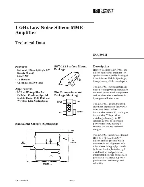
DescriptionHewlett-Packard’s INA-30311 is a Silicon monolithic amplifier for applications to 1.0 GHz. Packaged in a miniature SOT-143 package,it requires very little board space.The INA-30311 uses an internally biased topology which eliminates the need for external components and provides decreased sensitiv-ity to ground inductance.The INA-30311 is designed with an output impedance that varies from near 200 Ω at lowfrequencies to near 50 Ω at higher frequencies. This provides a matching advantage for IF circuits, as well as improved power efficiency, making it suitable for battery powered designs.The INA-30311 is fabricated using HP’s 30 GHz f MAX ISOSAT TM Silicon bipolar process which uses nitride self-alignment sub-micrometer lithography, trench isolation, ion implantation, gold metallization, and polyimide intermetal dielectric and scratch protection to achieve superior performance, uniformity, and reliability.1 GHz Low Noise Silicon MMIC Amplifier Technical DataINA-30311Features• Internally Biased, Single 3 V Supply (6 mA)• 3.5 dB NF • 13 dB Gain• Unconditionally StableApplications• LNA or IF Amplifier for Cellular, Cordless, Special Mobile Radio, PCS, ISM, and Wireless LAN ApplicationsSOT-143 Surface MountPackagePin Connections and Package MarkingEquivalent Circuit (Simplified)GNDOUTPUTINPUTV CCAbsolute Maximum RatingsAbsolute Symbol ParameterUnits Maximum [1]V CC Device Voltage, to ground V 12P in CW RF Input Power dBm +13T j Junction Temperature °C 150T STGStorage Temperature°C-65 to 150INA-30311 Electrical Specifications [3], T C = 25°C, Z O = 50 Ω, V CC = 3 VSymbol Parameters and Test ConditionsUnits Min.Typ.Max.G p Power Gain (|S 21|2) f = 900 MHz dB 1113NF Noise Figuref = 900 MHz dB 3.5P 1dB Output Power at 1 dB Gain Compression f = 900 MHz dBm -11IP 3Third Order Intercept Point f = 900 MHz dBm-2VSWR Input VSWR f = 900 MHz1.7I cc Device Current mA 6.37.5ιdGroup Delayf = 900 MHz ps 325INA-30311 Typical Scattering Parameters [3], T C = 25°C, Z O = 50 Ω, V CC = 3 VFreq.S 11S 21S 12S 22K GHz Mag Ang dB Mag Ang dB Mag Ang Mag Ang Factor 0.050.09-116.12 6.40-6-38.10.01220.57-1 4.350.100.09-216.11 6.39-12-38.20.01240.56-3 4.430.200.10-616.12 6.40-25-38.40.01280.56-7 4.410.300.13-1616.14 6.41-38-38.90.011130.55-11 4.830.400.16-2916.07 6.36-52-39.40.011190.54-14 4.880.500.18-4215.90 6.24-66-40.10.010270.52-18 5.600.600.21-5915.56 6.00-81-40.70.009400.50-20 6.580.700.22-7515.04 5.65-95-40.70.009570.47-237.260.800.24-9214.34 5.21-109-39.60.011740.46-24 6.490.900.25-10713.44 4.70-122-37.60.013860.44-24 6.231.000.26-12212.53 4.23-135-35.50.017940.43-25 5.351.200.27-14410.50 3.35-155-32.30.0241000.42-26 4.831.400.27-1628.50 2.66-173-29.60.0331010.42-27 4.431.600.27-177 6.69 2.16172-27.50.0421000.42-28 4.311.800.27173 5.01 1.78159-25.70.052990.42-30 4.222.000.27163 3.58 1.51147-24.10.062970.42-32 4.172.200.27156 2.35 1.31136-22.50.075950.42-35 3.972.400.26150 1.21 1.15126-21.40.085920.41-37 4.042.500.261470.751.09122-20.90.091910.41-393.99Note:3. Reference plane per Figure 9 in Applications Information section.Thermal Resistance [2]:θj-c = 550°C/WNotes:1. Operation of this device above any one of these limits may cause permanent damage.2. T C = 25°C (T C is defined to be thetemperature at the package pins where contact is made to the circuit board).INA-30311 Typical Performance, T C = 25°C, Z O = 50 Ω, V CC = 3 VFigure 7. Input and Output VSWR vs.Frequency.Figure 8. Supply Current vs. Voltage and Temperature.Figure 1. Power Gain vs. Frequency and Voltage.Figure 2. Noise Figure vs. Frequency and Voltage.G A I N (d B )0.10FREQUENCY (GHz)0.7201051.515 1.10.30.50.9 1.3 3.3 V 3.0 V 2.7 VN O I S E F I G U R E (d B )0.10FREQUENCY (GHz)0.74.02.01.0 1.53.0 1.10.30.50.9 1.3 2.7 V 3.0 V 3.3 V0.51.52.53.5P 1 d B (d B m )0.1-14FREQUENCY (GHz)0.70-6-10 1.5-4 1.10.30.50.9 1.33.3 V 3.0 V2.7 V -12-8-2V S W R (n :1)FREQUENCY (GHz)Figure 5. Noise Figure vs. Frequency and Temperature.Figure 6. Output Power for 1 dB Gain Compression vs. Frequency and Temperature.G A I N (d B )0.10FREQUENCY (GHz)0.7201051.515 1.10.30.50.9 1.3-40+25+85N O I S E F I G U R E (d B )0.10FREQUENCY (GHz)0.7521 1.541.10.30.50.9 1.3-40+25+853P 1 d B (d B m )0.1-12FREQUENCY (GHz)0.7-8-10-111.5-91.10.30.50.9 1.3-40+25+85Figure 3. Output Power for 1 dB Gain Compression vs. Frequency and Voltage.Figure 4. Gain vs. Frequency and Temperature.I C C (mA )V CC (V)INA-30311 Applications InformationIntroductionThe INA-30311 is a silicon RF integrated circuit that provides an easy-to-use solution for low noise or multi-purpose gain block applications up to 1000 MHz. This two-stage amplifier design uses resistive feedback to provide flat gain over a wide frequency range. This device is assembled in a miniature, surface mount package and is intended for use in low cost wireless communication products.A unique feature of the INA-30311 is that it is designed with a 50Ωinput impedance and an output impedance that approaches 200Ωat lower frequencies. This imped-ance converting feature is very useful for applications such as receiver IF circuits in which the INA-30311 is followed by highinput impedance devices like signal processing circuits, filters, or mixed signal ICs.In addition to simplifying the match to higher impedance devices, a key benefit of the higher output impedance feature is an improvement in power efficiency.Phase Reference PlanesThe positions of the reference planes used to measureS-Parameters are shown in Figure9. As seen in the illustra-tion, the reference planes are located at the point where the package leads contact the test circuit.MATCHEDΩOUTPUT BiasingThe INA-30311 is a voltage biaseddevice and operates from a single+3 volt power supply. With acurrent drain of 6 mA, thisamplifier is suitable for use inbattery powered applications. Allbias circuitry is fully integratedinto the IC eliminating the needfor external DC components. RFperformance is very stable for3-volt battery supplies that mayrange from 2.7 to 3.3 volts,depending on battery “freshness”or state of charge in the case ofrechargeable batteries.While the INA-30311 wasdesigned for use in +3 volt batterypowered applications, theinternal bias regulation circuitryallows it to be used with anypower supply voltage from +2.7to +5 volts.Typical ConfigurationsThe way in which the INA-30311is used depends on the particularapplication and operatingfrequency.• For receiver IF amplifier appli-cations up to several hundredMHz, the relatively higher out-put impedance level of theINA-30311 may be used toadvantage when interfacingdirectly with devices havinghigher than 50Ω input imped-ances, such as certain signalprocessing or mixed signal ICs.This application is shown inFigure 10.• A second implementation,shown in Figure 11, uses asimple reactive network at theamplifier’s output to match theoutput impedance to 50 Ω.This matched output arrangementwill provide an additional 0.9 dBof gain and output power at900MHz when driving into a 50Ωstage.• The third way to use the INA-30311 is to simply cascadeseveral INA-30311’s with 50Ωstages and neglect the effects ofthe output mismatch.The 50 Ω cascade withoutimpedance matching, shown inFigure 12, trades off theimprovement in stage gain andoutput power for a moresimplified interstage circuit andreduced circuit board space.Figure 11. Impedance MatchedOutput.Figure 12. Simple Cascade withoutImpedance Matching.Figure 10. INA-30311 Driving a HighInput Impedance Stage.RF RFFigure 13. Basic Amplifier Application.900 MHz Matched ExampleThis section describes ademonstration circuit for900␣MHz that is based on thematched output configurationshown in Figure11.The output VSWR of the INA-30311 is approximately 2.6:1 at900 MHz and results in a 0.9 dBmismatch loss when used in a50Ω system. The use of a simpleimpedance matching circuit at theoutput will increase both gain andoutput power by 0.9 dB. Thenoise figure of the amplifierremains the same and does notdepend on whether or not theoutput is matched.There are many circuit topologiesthat may be used to match theoutput impedance of theINA-30311 to a 50 Ω load. Theexample presented in Figure 15 isdesigned to match the amplifier’soutput for frequencies near900␣MHz.This circuit is representative forapplications in the 800 MHzcellular or 900 MHz unregulatedfrequency bands. This exampleuses a series capacitor to resonatewith a shunt, high impedancetransmission line. The transmis-sion line is tapped at a 50 Ω levelfor the output. This circuitprovides the desired impedancetransformation with a minimumof components, using only onechip capacitor that also doublesas the output DC block.used to the amplifier to the V CCsupply, additional bypasscapacitors may be needed toprevent resonances that wouldotherwise result in undesirablegain responses. A well-bypassedV CC line is also desirable toprevent possible oscillations thatmay occur due to feedbackthrough the bias line from otherstages in a cascade.Adequate grounding is needed toobtain maximum performance.The ground pin of the INA-30311should be connected to directlyto RF ground by using platedthrough holes (vias) near thepackage terminals.FR-4 or G-10 PCB material is agood choice for most low costwireless applications. Typicalboard thickness is 0.025 or0.031␣inches. The width of 50 Ωmicrostriplines in these PCBthicknesses is also convenient formounting chip components suchas the series DC blockingcapacitors.50 Ω ExampleThe demonstration circuit in Figure14 shows the INA-30311 usedwithout output impedancematching and is an example of thecascade depicted in Figure 12. Thislayout illustrates the simplestimplementation of the INA-30311by using 50 Ω microstriplineswith DC blocking capacitors forboth the input and output. TheV CC supply connection is RFbypassed very close to the lead ofthe RFIC. Provision is also madefor an additional bypass capacitoron the V CC line near the edge ofthe PCB.Operating DetailsThe basic application of the INA-30311 is shown in Figure 13. DC blocking capacitors should be placed in series with the RF Input and RF Output to isolate adjoin-ing circuits from the internal bias voltages that are present at these terminals. The values of the blocking capacitors are deter-mined by the lowest frequency of operation for a particular applica-tion. The capacitor’s reactances are chosen to be 5% or less of the amplifier’s input or output imped-ance at the lowest operating frequency. For example, an ampli-fier to be used in an application covering the 902 to 928 MHz band would require an input blocking capacitor of at least 70pF, which is 2.5 Ω of reactance, or 5% of50␣Ω at 902MHz.The V CC connection to the amplifier must be RF bypassed by placing a capacitor to ground directly at the bias pin of the package. Like the DC blocking capacitors, the value of the V CC bypass capacitor is determined by the lowest operating frequency for the ampli-fier. This value is typically the same as that of the DC blocking capacitors. If long bias lines areINA-30311 Part Number Ordering InformationPart Number Devices per ContainerContainer INA-30311-TR13,0007" reel INA-30311-BLK100Antistatic bagFigure 14. 50 Ω Input/Output Example.Figure 15. Matched Output Example.DIMENSIONS ARE IN MILLIMETERS (INCHES)0.10 (0.004) 0.013 (0.0005)END VIEWSIDE VIEWPackage Dimensions。