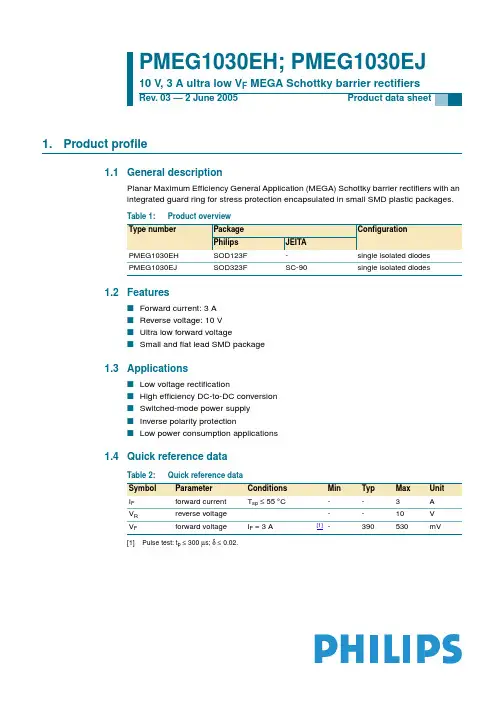
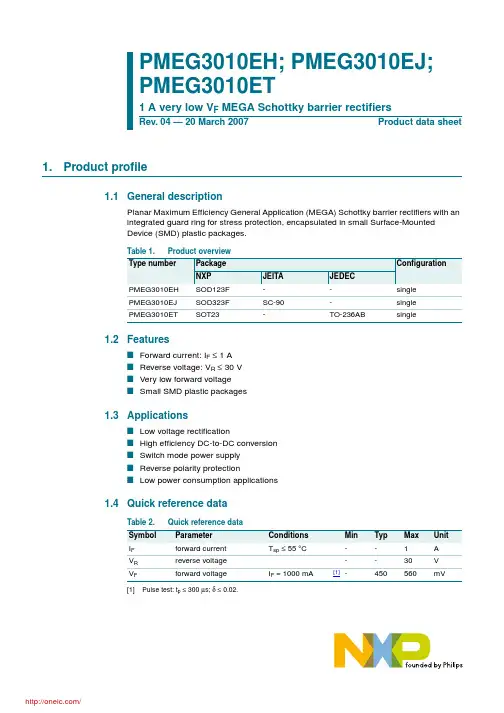
Product Data Sheet DS656The Bridgelux SMD 3030 high power LED is hot-color targeted, which ensures that the LEDs fall within their specified color bin at the typical application conditions of 85°C. With its broad lumen coverage and wide range of CCT options, the SMD 3030 provides unparalleled design-in flexibility for indoor and outdoor lighting applications. The SMD 3030 is ideal as a drop-in replacement for emitters with an industry standard 3.0mm x 3.0mm footprint.Features• Industry-standard 3030 footprint• 5 bin color control• Hot-color targeting ensures that color is within the ANSI bin at the typical application conditions of 85°C • Enables 3- and 6-step MacAdam ellipse custom binning kits• RoHS compliant and lead free• Multiple CCT configurations for a wide range of lighting applicationsBenefits• Lower operating and manufacturing cost • Ease of design and rapid go-to-market • Uniform, consistent white light• Reliable and constant white point• Compliant with environmental standards • Design flexibilityContentsProduct Feature Map2 Product Nomenclature2 Product Test Conditions2 Product Selection Guide3 Electrical Characteristics4 Absolute Maximum Ratings5 Product Bin Definitions6 Performance Curves9 Typical Radiation Pattern12 Typical Color Spectrum 13 Mechanical Dimensions14 Reliability 15 Reflow Characteristics16 Packaging17 Design Resources19 Precautions19 Disclaimers19 About Bridgelux20Product Feature MapCathode MarkYellow phosphor Light Emitting Surface (LES)Product NomenclatureThe part number designation for Bridgelux SMD 3030 is explained as follows:Product Test ConditionsBridgelux SMD 3030 LEDs are tested and binned with a 10ms pulse of 100mA at Tj (junction temperature)=T sp (solder point temperature) =25°C. Forward voltage and luminous flux are binned at a T j =T sp =25°C.while color is hot targeted at a T sp of 85°C.1 2 3 4 5 6 7 8 9 10 11 12 13 14 15 16 17Product FamilyColor Bin OptionsFlux Bins Minimum CRIE = 80 CRIForward Voltage Bins Nominal CCT27 = 2,700K 30 = 3,000K 35 = 3,500K 40 = 4,000K 50 = 5,000K 57 = 5,700K 65 = 6,500KBXEM – 30 E – 1 3 H – 9 CS – 00 – 0 – 0Product Version High PowerDie count in parallelTypical Forward VoltageDie count in series Bridgelux SMD LED products come in industry standard package sizes and follow ANSI binning standards. These LEDs are optimized for cost and performance, helping to ensure highly competitive system lumen per dollar performance while addressing the stringent efficacy and reliability standards required for modern lighting applications.Product Selection GuideThe following product configurations are available:Table 1: Selection Guide, Pulsed Measurement Data at 100mA (T j =T sp =25°C)Notes for Tables 1 & 2:1. The last 6 characters (including hyphens ‘-’) refer to flux bins, forward voltage bins, and color bin options, respectively. “00-0-0” denotes the full distribution of flux, forward voltage, and 6 SDCM color.Example: BXEM-30E-13H-9CS-00-0-0 refers to the full distribution of flux, forward voltage, and color within a 3000K 6-step ANSI standard chromaticity region with a minimum of 80CRI, 1x3 die configuration, 8.9V typical forward voltage.2. Product CCT is the nominal CCT at Tsp = 85°C as defined by ANSI C78.377-2011.3. Listed CRIs are minimum values at Tsp = 85°C and include test tolerance.4. Products tested under pulsed condition (10ms pulse width) at nominal drive current where Tj=Tsp=25°C.5. Bridgelux maintains a ±7.5% tolerance on luminous flux measurements, ±0.1V tolerance on forward voltage measurements, and ±2 tolerance on CRI measurements for the SMD 3030.6. Refer to Table 5 and Table 6 for Bridgelux SMD 3030 Luminous Flux Binning and Forward Voltage Binning information.7. Typical pulsed test performance values are provided as reference only and are not a guarantee of performance.8. Typical performance is estimated based on operation under pulsed current with LED emitter mounted onto a heat sink with thermal interfacematerial and the solder point temperature maintained at 85°C. Based on Bridgelux test setup, values may vary depending on the thermal design of the luminaire and/or the exposed environment to which the product is subjected.Table 2: Selection Guide, Pulsed Test Performance (T sp = 85°C)7,8Electrical CharacteristicsTable 3: Electrical CharacteristicsNotes for Table 3:1. The last 6 characters (including hyphens ‘-’) refer to flux bins, forward voltage bins, and color bin options, respectively. “00-0-0” denotes the full distribution of flux, forward voltage, and 6 SDCM color.Example: BXEM-30E-13H-9CS-00-0-0 refers to the full distribution of flux, forward voltage, and color within a 3000K 6-step ANSI standardchromaticity region with a minimum of 80CRI, 1x3 die configuration, high power, 8..9V typical forward voltage.2. Bridgelux maintains a tolerance of ± 0.1V on forward voltage measurements. Voltage minimum and maximum values at the nominal drive current are guaranteed by 100% test.3. Products tested under pulsed condition (10ms pulse width) at nominal drive current where Tsp = 25°C.4. Thermal resistance value was calculated using total electrical input power; optical power was not subtracted from input power.Absolute Maximum RatingsTable 4: Maximum RatingsNotes for Table 4:1. Bridgelux recommends a maximum duty cycle of 10% and pulse width of 10 ms when operating LED SMD at maximum peak pulsed current specified.Maximum peak pulsed current indicate values where LED SMD can be driven without catastrophic failures.2. Light emitting diodes are not designed to be driven in reverse voltage and will not produce light under this condition. no rating is providedProduct Bin DefinitionsTable 5:Luminous flux Bin Definitions at 100mA, T sp =25°CTable 5 lists the standard photometric luminous flux bins for Bridgelux SMD 3030 LEDs. Although several bins are listed, product availability in a particular bin varies by production run and by product performance. Not all bins are available in all CCTs.Table 6: Forward Voltage Bin Definition at 100mA, T sp=25°CNote for Table 6:1. Bridgelux maintains a tolerance of ± 0.1V on forward voltage measurements.Note for Table 5:1.Bridgelux maintains a tolerance of ± 7.5% on luminous flux measurements.Product Bin DefinitionsTable 7: 3- and 6-step MacAdam Ellipse Color Bin DefinitionsNotes for Table 7:1. Color binning at T=85°C unless otherwise specifiedsp2. Bridgelux maintains a tolerance of ± 0.007 on x and y color coordinates in the CIE 1931 color space.Product Bin DefinitionsFigure 1: C.I.E. 1931 Chromaticity Diagram (5 Color Bin Structure, Hot-color Targeted at Tsp=85°C)Note for Figure 3:1. Pulse width modulation (PWM) is recommended for dimming effects.Figure 2: Drive Current vs. Voltage (T sp =25°C)Figure 4: Typical Relative Flux vs. Solder Point TemperatureFigure 5: Typical ccx Shift vs. Solder Point TemperatureNotes for Figures 4 & 5:1. Characteristics shown for neutral white based on 4000K 80 CRI.2. For other color SKUs, the shift in color will vary. Please contact your Bridgelux Sales Representative for more information.Figure 6: Typical ccy Shift vs. Solder Point TemperatureD r a2. For other color SKUs, the shift in color will vary. Please contact your Bridgelux Sales Representative for more information.Typical Radiation PatternFigure 7: Typical Spatial Radiation Pattern at 100mA, T sp =25°CFigure 8: Typical Polar Radiation Pattern at 100mA, T sp =25°CNotes for Figure 7:1. Typical viewing angle is 120⁰.2. The viewing angle is defined as the off axis angle from the centerline where luminous intensity (Iv) is ½ of the peak value.Typical Color Spectrum Figure 9: Typical Color SpectrumNotes for Figure 9:1. Color spectra measured at nominal current for Tsp = 25°C2. Color spectra shown for 80 CRI products.Mechanical Dimensions Figure 10: Drawing for SMD 3030Notes for Figure 10:1. Drawings are not to scale.2. Drawing dimensions are in millimeters.3. Unless otherwise specified, tolerances are ± 0.10mm. Recommended PCB Soldering Pad PatternReliabilityTable 8: Reliability Test Items and ConditionsNotes for Table 8:1. Measurements are performed after allowing the LEDs to return to room temperature2. T sld : reflow soldering temperature; T a: ambient temperaturePassing CriteriaFigure 11 : Reflow ProfileReflow CharacteristicsFigure 12 : Pick and PlaceNote for Figure 12:1. When using a pick and place machine, choose a nozzle that has a larger diameter than the LED’s emitting surface. Using a Pick-and-Place nozzle witha smaller diameter than the size of the LEDs emitting surface will cause damage and may also cause the LED to not illuminate.Is greater than LEDsemitting surfacePackagingFigure 13: Emitter Reel DrawingsNote for Figure 13:1. Drawings are not to scale. Drawing dimensions are in millimeters. Figure 14: Emitter Tape DrawingsNote for Figure 14:1. Drawings are not to scale. Drawing dimensions are in millimeters.PackagingFigure 15: Emitter Reel Packaging DrawingsNote for Figure 15:1.Drawings are not to scale.5 k10 kDesign ResourcesDisclaimersPrecautionsPlease contact your Bridgelux sales representative for assistance.MINOR PRODUCT CHANGE POLICYThe rigorous qualification testing on products offered by Bridgelux provides performance assurance. Slight cosmetic changes that do not affect form, fit, or function may occur as Bridgelux continues product optimization.CAUTION: CHEMICAL EXPOSURE HAZARDExposure to some chemicals commonly used in luminaire manufacturing and assembly can cause damage to the LED emitter. Please consult Bridgelux Application Note AN51 for additional information.CAUTION: EYE SAFETYEye safety classification for the use of Bridgelux SMD LED emitter is in accordance with IECspecification EN62471: Photobiological Safety of Lamps and Lamp Systems. SMD LED emitters are classified as Risk Group 1 when operated at or belowthe maximum drive current. Please use appropriate precautions. It is important that employees working with LEDs are trained to use them safely.CAUTION: RISK OF BURNDo not touch the SMD LED emitter during operation. Allow the emitter to cool for a sufficient period of time before handling. The SMD LED emitter may reachelevated temperatures such that could burn skin when touched.CAUTIONCONTACT WITH LIGHT EMITTING SURFACE (LES) Avoid any contact with the LES. Do not touch the LES of the emitter or apply stress to the LES (yellow phosphor resin area). Contact may cause damage to the emitterOptics and reflectors must not be mounted in contact with the LES (yellow phosphor resin area).STANDARD TEST CONDITIONSUnless otherwise stated, LED emitter testing is performed at the nominal drive current.About Bridgelux: Bridging Light and Life™© 2021 Bridgelux, Inc. All rights reserved 2021. Product specifications are subject to change without notice. Bridgelux and the Bridgelux stylized logo design are registered trademarks of Bridgelux, Inc. All other trademarks are the property of their respective owners.46410 Fremont Boulevard Fremont, CA 94538 USA Tel (925) 583-8400Fax (925) At Bridgelux, we help companies, industries and people experience the power and possibility of light. Since 2002, we’ve designed LED solutions that are high performing, energy efficient, cost effective and easy to integrate. Our focus is on light’s impact on human behavior, delivering products that create better environments, experiences and returns—both experiential and financial. And our patented technology drives new platforms for commercial and industrial luminaires.For more information about the company, please visit /Bridgelux /Bridgelux/user/Bridgelux WeChat ID: BridgeluxInChina https:///company/bridgelux-inc-_2。