
26-423_ZH_TI_PCD1-PCD2
- 格式:pdf
- 大小:11.72 MB
- 文档页数:20
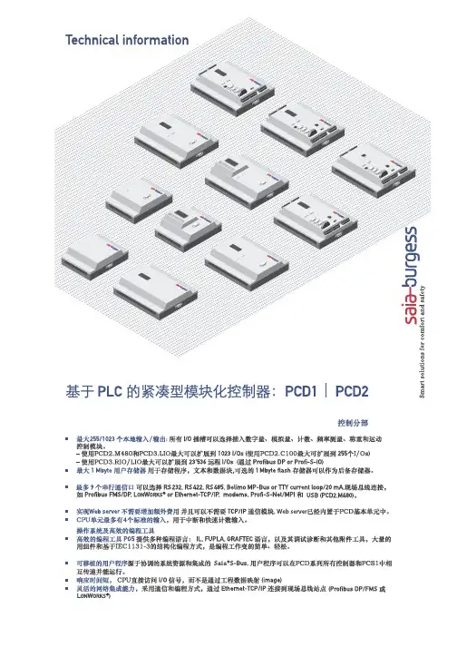

DS-2SE7C432MWG-EB/26(F0)TandemVu 4 MP 32 × Network PTZ Camera⏹Panoramic channel supports image stitching, with 180°horizontal field of view⏹High quality imaging with 6 MP resolution inpanoramicand channel and 4 MP resolution in PTZchannel⏹Secures an expansive area with 32 × optical zoom and 16 ×digital zoom⏹AcuSense technology focuses on human and vehicletargets classification and supports face capture to detect,capture and select faces in motion⏹Expansive night view with up to 200 m IR distance in PTZchannel and 30 m white light in panoramic channel⏹Active strobe light and audio alarm to warn intruders off⏹Smart-linkage between panoramic channel and PTZchannelSpecification CameraImage Sensor [Panoramic channel] 1/2.5" Progressive Scan CMOS [PTZ channel] 1/2.8" Progressive Scan CMOSShutter Speed 1 s to 1/30,000 sMin. Illumination [PTZ channel] Color: 0.005 Lux @ (F1.5, AGC ON), B/W: 0.001 Lux @ (F1.5, AGC ON), 0 lux with IR[Panoramic channel] Color: 0.0005 Lux @ (F1.0, AGC ON), 0 Lux with LightSlow Shutter yesDay &Night IR cut filterHLC yes3D DNR yesWhite Balance auto,ATW,sodium lamp,fluorescent lamp,indoor,outdoor,MWB,Locked WB Zoom 32 × optical,16 × digitalMax. Resolution [Panoramic channel] 3632 × 1632 [PTZ channel] 2560 × 1440LensFOV [Panoramic channel] horizontal field of view: 180°±10°, vertical field of view: 80°±5°[PTZ channel] horizontal field of view: 60.2° to 2.3°Focus Auto,semi-auto,manualZoom Speed [Panoramic channel] No [PTZ channel] approx. 5.6 sFocal Length [Panoramic channel] 2.8 mm [PTZ channel] 5.9 to 188.8 mmAperture [Panoramic channel] F1.0 [PTZ channel] Max. F1.5IlluminatorWhite Light Distance Panoramic channel: 30 mSupplement Light Range IR distance: up to 200 mPTZMovement Range (Pan) 360°Movement Range (Tilt) -15° to 90°Pan Speed Pan speed: configurable from 0.1° to 160°/s, preset speed: 240°/s Tilt Speed Tilt speed: configurable from 0.1° to 120°/s, preset speed 200°/s Proportional Pan YesPresets 300Patrol Scan 8 patrols, up to 32 presets for each patrolPattern Scan 4 pattern scans, record time over minutes for each scan Power-off Memory YesPark Action Preset,pattern scan,patrol scan,auto scan,tilt scan,random scan,frame scan,panorama scan3D Positioning Yes PTZ Status Display Yes Preset Freezing YesScheduled Task Preset,pattern scan,patrol scan,auto scan,tilt scan,random scan,frame scan,panorama scan,dome reboot,aux output,dome adjustVideoStream Type main stream,sub-stream,third streamMain Stream [PTZ channel] 50 Hz: 25 fps (2560 × 1440, 1920 × 1080, 1280 × 960, 1280 × 720), 60 Hz: 30 fps (2560 × 1440, 1920 × 1080, 1280 × 960, 1280 × 720)[Panoramic channel] 50 Hz: 25 fps (3632 × 1632, 3680 × 1656), 60 Hz: 30 fps (3632 × 1632, 3680 × 1656)Sub-Stream [PTZ channel] 50 Hz: 25 fps (704 × 576, 640 × 480, 352 × 288), 60 Hz: 30 fps (704 × 480, 640 × 480, 352 × 240)[Panoramic channel] 50 Hz: 25 fps (1200 × 536, 960 × 432), 60 Hz: 30 fps (1200 × 536, 960 × 432)Third Stream [PTZ channel] 50 Hz: 25 fps (1920 × 1080, 1280 × 960, 1280 × 720, 704 × 576, 640 × 480, 352 × 288), 60 Hz: 30 fps (1920 × 1080, 1280 × 960, 1280 × 720, 704 × 480, 640 × 480, 352 × 240)[Panoramic channel] NoVideo Compression Main stream: H.265+/H.265/H.264+/H.264, Sub-stream: H.265/H.264/MJPEG,Third stream: H.265/H.264/MJPEGVideo Bit Rate 32 Kbps to 16384 MbpsH.264 Type Baseline Profile,Main Profile,High ProfileH.265 Type Main ProfileScalable Video Coding (SVC) yesRegion of Interest (ROI) fixed regionAudioAudio Compression G.711,G.722.1,G.726,MP2L2,PCM,AAC-LC,MP3Audio Bit Rate 32 to 192 Kbps (MP2L2),16 to 64Kbps (AAC-LC),8 to 320 Kbps (MP3)Audio Sampling Rate MP2L2: 16kHz, 32kHz, 48kHz AAC-LC: 16kHz, 32kHz, 48kHz PCM: 8kHz, 16kHz, 32kHz, 48kHz MP3: 8kHz, 16KHz, 32KHz, 48KHzEnvironment Noise Filtering yesSmart FeaturesSmart Record ANR (Automatic Network Replenishment), Dual-VCA NetworkProtocols TCP/IP,ICMP,HTTP,HTTPS,FTP,DHCP,DNS,DDNS,RTP,RTSP,RTCP,PPPoE,NTP,UPnP,SMTP ,SNMP,IGMP,802.1X,QoS,IPv4/IPv6,UDP,Bonjour,WebSocket,WebSockets,SRTPNetwork Storage NAS (NFS, SMB/CIFS),auto network replenishment (ANR) API ISUP,SDK,ISAPI,ONVIF (Profile S, Profile G, Profile T) Simultaneous Live View 20User/Host 32Security Password protection,HTTPS encryption,802.1X authentication (EAP-TLS, EAP-LEAP, EAP-MD5),host authentication (MAC address),IP address filterClient iVMS-4200,HikCentral Pro,Hik-ConnectWeb Browser IE 11+, Chrome 57+, Firefox 52+, Safari 12+, Edge79.0.309.65+ ImageWide Dynamic Range (WDR) [Panoramic channel] Digital WDR [PTZ channel] 120 dBDay/Night Switch Day,night,auto,scheduleImage Enhancement BLC,HLC,3D DNRDefog yesImage Stabilization yesRegional Exposure yesRegional Focus yesImage Settings saturation, brightness, contrast, sharpnessImage Parameters Switch YesPrivacy Mask 24 programmable polygon privacy masks, mask color or mosaic configurableSNR >52dBInterfaceEthernet Interface 1 RJ45 10/100M self-adaptive Ethernet portOn-board Storage Built-in memory card slot, support Micro SD/Micro SDHC/Micro SDXC, up to 512 GB Alarm 2 input(s), 1 output(s)Audio 1 input (line in), max. input amplitude: 2-2.4 vpp, input impedance: 1 KΩ ± 10%, 1 output (line out), line level, output impedance: 600 ΩReset Yes EventBasic Event Motion detection,video tampering alarm,alarm input and output,exception (network disconnected, IP address conflict, illegal login, HDD full, HDD error, abnormal restart)Smart Event Line crossing detection,intrusion detection,region entrance detection,region exiting detection,audio exception detectionLinkage Upload to FTP/NAS/memory card,notify surveillance center,send email,trigger alarm output,trigger recording,and PTZ actions (such as preset, patrol scan, pattern scan),audible warning,white light flashingSmart Linkage panorama linkage, tracking takeover, track in turn Smart Tracking Manual tracking,auto-trackingDeep Learning FunctionFace Capture Support detecting up to 5 faces at the same time. Support detecting, capturing, grading, selecting of face in motion, and output the best face picture of the faceGeneralPower 24 VAC, Max. 60 W, Hi-PoEMaterial ADC12,Plastic,PC+10%GFGeneral Function mirror,watermark,password protection,IP address filterOperating Condition -30 °C to 65 °C (-22 °F to 149 °F). Humidity 90% or less (non-condensing)Demist YesDimension Ø222.3 mm × 387.2 mm (Ø8.75" × 15.2")Weight Approx. 4.75 kg (10.47 lb.)ApprovalProtection IP66 (IEC 60529-2013)DORIThe DORI (detect, observe, recognize, identify) distance gives the general idea of the camera ability to distinguish persons or objects within its field of view. It is calculated based on the camera sensor specification and the criteria given by EN 62676-4: 2015.DORI Detect Observe Recognize Identify Definition 25 px/m 63 px/m 125 px/m 250 px/m Distance (Tele)3060.0 m (10039.4 ft.)1214.3 m (3983.9 ft.)612 m (2007.9 ft.)306.0 m (1004.0 ft.)⏹Dimension⏹Accessory⏹OptionalDS-1602ZJ-PoleDS-1681ZJ-2DS-1661ZJDS-1602ZJDS-1602ZJ-CornerDS-2681ZJ⏹Available ModelDS-2SE7C432MWG-EB/26(F0)。

(1-x)PST-xPZT铁电陶瓷的介电与热释电性能研究1蓝德均、江一杭、陈异、陈强、肖定全、朱建国*(四川大学材料科学与工程学院 四川成都 610064)E-mail: nic0400@摘要:以普通氧化物混合烧结法制备了高钙钛矿相的(1-x)PST-xPZT铁电弛豫陶瓷。
发现烧结温度和PZT掺入量对样品中的焦绿石相的存在影响很大。
样品的钙钛矿相成分随烧结温度升高而增加。
介电性能测试表明(1-x)PST-xPZT铁电弛豫陶瓷具有弥散型介电响应特征,(1-x)PST-xPZT铁电弛豫陶瓷的居里点T c和压电常数d33随PZT的掺入量的增加而增加。
室温下x=0.1的(1-x)PST-xPZT陶瓷样品的热释电系数可达到约15×10-8C/(cm2.K)。
关键词:PST-PZT陶瓷;弛豫铁电陶瓷;钙钛矿相;一步烧结制备1.引言钽钪酸铅Pb(Sc1/2Ta1/2)O3(PST)是一种热释电性能优良的典型B位复合铅基钙钛矿弛豫铁电陶瓷[1~3]。
由于纯PST的居里点较低(-5℃-25℃),需要在约1500℃的高温下烧结才能获得致密、具有钙钛矿结构且性能良好的材料[4],从而限制了PST陶瓷材料的应用领域。
为了避免会引起陶瓷性能恶化的焦绿石相的形成,通常制备B位复合铅基钙钛矿驰豫铁电陶瓷的方法是先驱体法,即先将B位化合物或一种B位组份与一种A位组份[5]先行在高温下进行焙烧,制备出一种中间材料后再将组成陶瓷的其它组份化合物与前驱体混合后烧结得到所需的陶瓷。
但是有也研究表明[6,7],用传统电子陶瓷制备工艺(以下简称一步法,One-Step-Sintering Method,OSSM),也可以制备出B位复合纯钙钛矿相陶瓷材料。
由于一般二元系的准同型相界(Morphotropic Phase Boundary,MPB)是一个范围很窄的区间,通过MPB成分的调整而达到调整材料综合性能的自由度很小;但对于三元或更多元系来说,其准同型相界一般是曲线甚至是曲面,故而在MPB附近进行组分调控可望进一步优化材料的综合性能[8]。

Features Array•AM/FM Tuner Front End with Integrated PLL•AM Up-conversion System (AM-IF: 10.7MHz)•FM Down-conversion System (FM-IF: 10.7MHz)•IF Frequencies up to 25MHz•Fine-tuning Steps: AM=1kHz and FM=50kHz/25kHz/12.5kHz•Fast Fractional PLL (Lock Time < 1ms) Inclusive Spurious Compensation•Fast RF-AGC, Programmable in 1-dB Steps•Fast IF-AGC, Programmable in 2-dB Steps•Fast Frequency Change by 2 Programmable N-divider•Two DACs for Automatic Tuner Alignment•High S/N Ratio•3-wire Bus (Enable, Clock and Data; 3V and 5V Microcontrollers-compatible)1.DescriptionThe T4260 is an advanced AM/FM receiver with integrated fast PLL as a single-chip solution based on Atmel®’s high-performance BICMOS II technology. The low-imped-ance driver at the IF output is designed for the A/D of a digital IF. The fast tuning concept realized in this part is based on patents held by Atmel and allows lock times less than 1ms for a jump over the FM band with a step width of 12.5kHz. The AM up-conversion and the FM down-conversion allows an economic filter concept. An automatic tuner alignment is provided by built-in DACs for gain and offset compensa-tion. The frequency range of the IC covers the FM broadcasting band as well as the AM band. The low current consumption helps the designers to achieve economicpower consumption concepts and helps to keep the power dissipation in the tuner low.24528M–AUDR–03/08T4260Figure 1-1.Block Diagram34528M–AUDR–03/08T42602.Pin ConfigurationFigure 2-1.Pinning SSO44Table 2-1.Pin DescriptionPin Symbol Function 1DAC1DAC1 output 2DAC2DAC2 output 3FMAGCO FM AGC current 4MXFMIA FM mixer input A 5MXFMIB FM mixer input B 6GNDRF RF ground7MXAMIB AM mixer input B 8MXAMIA AM mixer input A 9AMAGCO AM AGC current 10IFAGCA2AM IF-AGC filter 211SW2/AGC Switch 2/AM AGC voltage 12RFAGCA2RF AM-AGC filter 213SW1Switching output 114VRVCO VCO reference voltage 15VSPLL PLL supply voltage 16FMLF FM loop filter 17AMLF AM loop filter 18VTUNE Tuning voltage 19OSCGND Oscillator ground 20OSCEOscillator emitter44528M–AUDR–03/08T42603.Functional DescriptionThe T4260 implements an AM up-conversion reception path from the RF input signal to the IF output signal. A VCO and an LO prescaler for AM are integrated to generate the LO frequency to the AM mixer. The FM reception path generates the same LO frequency from the RF input sig-nal by a down-conversion to the IF output. The IF A/D output is designed for digital signal processing. The IF can be chosen in the range of 10MHz to 25MHz. Automatic gain control (AGC) circuits are implemented to control the preamplifier stages in the AM and FM reception paths.For improved performance, the PLL has an integrated special 2-bit shift fractional logic with spu-rious suppression that enables fast frequency changes in AM and FM mode by a low step frequency (f PDF ). In addition, two programmable DACs (Digital to Analog Converter) support the alignment via a microcontroller.For a double-tuner concept, external voltage can be applied at the input of the DACs, the inter-nal PLL can switched off and the OSC buffer (output) can also be used as input.Several register bits (bit 0 to bit 145) are used to control the circuit’s operation and to adapt cer-tain circuit parameters to the specific application. The control bits are organized in four 8-bit, four 16-bit and three 24-bit registers that can be programmed by the 3-wire bus protocol. The bus protocol and the bit-to-register mapping is described in Section 8. “3-wire Bus Description” on page 10. The meaning of the control bits is mentioned in the following sections.21OSCB Oscillator base22OSCBUF Oscillator buffer output/input 23EN 3-wire bus Enable 24CLK 3-wire bus Clock 25DA TA 3-wire bus Data26VRPLL PLL reference voltage 27REFFREQ PLL reference frequency 28GNDPLL PLL ground 29IFOUTB IF output B 30IFOUTA IF output A31IFAGCFM FM IF-AGC filter 32IFAGCA1AM IF-AGC filter 133RFAGCFM RF FM-AGC filter34IFREF IF amplifier reference input 35IFINAM IF amplifier AM input 36IFINFM IF amplifier FM input 37VRT Tuner reference voltage 38GNDT Tuner ground39MXAMOB AM mixer output B 40MXAMOA AM mixer output A 41VST Tuner supply voltage 42RFAGCA1RF AM-AGC filter 143MXFMOA FM mixer output A 44MXFMOBFM mixer output BTable 2-1.Pin Description (Continued)Pin Symbol Function54528M–AUDR–03/08T42604.Absolute Maximum RatingsStresses beyond those listed under “Absolute Maximum Ratings” may cause permanent damage to the device. This is a stress rating only and functional operation of the device at these or any other conditions beyond those indicated in the operational sections of this specification is not implied. Exposure to absolute maximum rating conditions for extended periods may affect device reliability.All voltages are referred to GND ParametersSymbol Value Unit Analog supply voltage, pins 15 and 41V ST , V SPLL10V Maximum power consumption P tot 1.0W Ambient temperature range T amb –40 to +85°C Storage temperature range T stg –40 to +150°C Junction temperatureT j150°C5.Thermal ResistanceParametersSymbol Value Unit Junction ambient, soldered to PCBR thJA52K/W6.Operating RangeParametersSymbol Min.Typ.Max.Unit Supply voltage range (1), pins 15 and 41V ST , V SPLL88.510V Ambient temperature T amb –4085°C Oscillator frequency, pin 21R fi60175MHzNote:1.V ST and V SPLL must have the same voltage.7.Electrical CharacteristicsT est conditions (unless otherwise specified): V ST /V SPLL = +8.5V , T amb = +25°C No.Parameters Test ConditionsPinSymbolMin.Typ.Max.UnitType*1PowerSupply 1.1Supply voltage 15, 41V S 88.510V C 1.2Supply current AM and FM mode,V S = 10V15, 41I S7085110mAA2PLL Divider 2.1Programmable R-divider14-bit register 316383A 2.2Programmable (VCO) N-divider(1 kHz step frequency)2-bit ×18-bit register switchable via bit 53262143A 2.3Reference oscillator input voltage f = 0.1MHz to 3MHz 27100mV rms B2.4Reference frequencyFM AM12012015028501000010000kHz kHz*) T ype means: A = 100% tested, B = 100% correlation tested, C = Characterized on samples, D = Design parameter Note:1.Minimum and maximum limits are characterized for entire temperature range (–40°C to +85°C) but are tested at +25°C64528M–AUDR–03/08T42602.5Settling time in FM mode (switching from87.5MHz to 108MHz or vice versa)f PD = 50 kHz I PD = 2 mA1msB3AMLF/FMLF 3.1Output current 1FMLF , AMLF =1.8V 16, 17405060µA A (1)3.2Output current 2FMLF , AMLF =1.8V 16, 1780100120µA A (1)3.3Output current 3FMLF , AMLF =1.8V 16, 1785010001250µA A (1)3.4Output current 4FMLF , AMLF =1.8V 16, 17165020002450µA A (1)3.5Leakage current FMLF , AMLF =1.8V16, 1710nAA (1)4VTUNE4.1Saturation voltage LOWV SA TL = V TUNEMIN 18V SATL 100200400mV C 4.2Saturation voltage HIGH V SA TH =V SPLL - V TUNEMAX18V SA TH500mVC5DAC1, DAC25.1Output current 1, 2I DAC1,21mA D 5.2Output voltage 1, 2V DAC1,20.3V S –0.6V A 5.3Maximum offset range Offset = 0, gain = 581, 20.90.98 1.1V A (1)5.4Minimum offset range Offset = 127, gain = 581, 2–0.9–0.98–1.1V A (1)5.5Maximum gain range Gain = 255, offset = 641, 2 2.06 2.09 2.13–A (1)5.6Minimum gain range Gain = 0, offset = 641, 20.630.670.73–A (1)6Oscillator 6.1Frequency range 2160170MHz B 6.2Fractional frequency range Fractional mode2160140MHz A 6.3Buffer output 22150mV rms C 6.4Buffer input Slave mode 22100mV rms C 6.5Input voltage 21V OSC150mV rmsA7FM Mixer 7.1Frequency range 75163MHz B 7.2Input IP3133dBµV C 7.3Input impedance 3.5k ΩD 7.4Input capacitance 4pF D 7.5Noise figure F14dB C 7.6Conversiontransconductance2.63.13.6msD (1)7.Electrical Characteristics (Continued)T est conditions (unless otherwise specified): V ST /V SPLL = +8.5V , T amb = +25°C No.ParametersTest Conditions PinSymbolMin.Typ.Max.Unit Type**) T ype means: A = 100% tested, B = 100% correlation tested, C = Characterized on samples, D = Design parameter Note:1.Minimum and maximum limits are characterized for entire temperature range (–40°C to +85°C) but are tested at +25°C74528M–AUDR–03/08T42608AM Mixer (Symmetrical Input)8.1Frequency range 0.07526MHz B 8.2Input IP3133dBµV C 8.3Input impedance 2.5k ΩD 8.4Noise figure F10dB C 8.5Conversiontransconductance 2.63.13.6mSD (1)9Isolation 9.1Isolation AM-FM 40dB C 9.2IF suppression 40dBC10RF-AGC 10.1Frequency range FM AM 750.07516326MHz MHz A 10.2Output current FM AM55mA mA B 10.3Output current time constantFM rising FM fallingAM symmetrical 25040ms ms ms C 10.4RF-AGC AM threshold (programmable with bit 12-bit 15)88 dBµV 42878890dBµV A (1)89 dBµV 42888991dBµV A (1)90 dBµV 42899092dBµV A (1)91 dBµV 42909193dBµV A (1)92 dBµV 42919294dBµV A (1)93 dBµV 42929395dBµV A (1)94 dBµV42939496dBµV A (1)95 dBµV 42949597dBµV A (1)96 dBµV 42959698dBµV A (1)97 dBµV 42969799dBµV A (1)98 dBµV 429798100dBµV A (1)99 dBµV 429899101dBµV A (1)100 dBµV 4299100102dBµV A (1)101 dBµV 42100101103dBµV A (1)102 dBµV 42101102104dBµV A (1)103 dBµV42102103107dBµVA (1)7.Electrical Characteristics (Continued)T est conditions (unless otherwise specified): V ST /V SPLL = +8.5V , T amb = +25°C No.Parameters Test ConditionsPinSymbolMin.Typ.Max.Unit Type**) T ype means: A = 100% tested, B = 100% correlation tested, C = Characterized on samples, D = Design parameterNote:1.Minimum and maximum limits are characterized for entire temperature range (–40°C to +85°C) but are tested at +25°C84528M–AUDR–03/08T426010.5RF-AGC FM threshold (programmable with bit 12-bit 15)91 dBµV 33909193dBµV A (1)92 dBµV 33919295dBµV A (1)93 dBµV 33929396dBµV A (1)94 dBµV 33939496dBµV A (1)95 dBµV 33949598dBµV A (1)96 dBµV 33959699dBµV A (1)97 dBµV339697102dBµV A (1)98 dBµV 339798101dBµV A (1)99 dBµV 339899102dBµV A (1)100 dBµV 3399100104dBµV A (1)101 dBµV 33100101104dBµV A (1)102 dBµV 33101102105dBµV A (1)103 dBµV 33102103106dBµV A (1)104 dBµV 33103104107dBµV A (1)105 dBµV 33104105108dBµV A (1)106 dBµV33105106109dBµVA (1)11IF Amplifier 11.1Frequency range 1025MHz A 11.2Output voltage 117dBµV B 11.3Distortion (2-tone IM3)f1 = 10.7 MHz f2 = 10.75 MHz RL = 2 × 300Ω55dB A 11.4Gain (programmable in 2-dB steps)Minimum gain Maximum gain 1242dB dB A 11.5Input impedance FM AM36, 353302500ΩΩD12IF-AGC12.1IF-AGCAM/FM threshold(programmable with bit 0 - bit 2)109 dBµV 29/30108109112dBµV A (1)111 dBµV29/30110111114dBµV A (1)113 dBµV 29/30111113115dBµV A (1)115 dBµV 29/30113115117dBµV A (1)117 dBµV 29/30116117121dBµV A (1)118 dBµV 29/30117118122dBµV A (1)119 dBµV 29/30118119123dBµV A (1)121 dBµV29/30120121126dBµV A (1)12.2AGC dynamic range 40dB B 12.3AGC time constant (external capacity ≤100nF)FM rising FM fallingAM symmetrical164200µs ms msD7.Electrical Characteristics (Continued)T est conditions (unless otherwise specified): V ST /V SPLL = +8.5V , T amb = +25°C No.ParametersTest Conditions Pin SymbolMin.Typ.Max.Unit Type**) T ype means: A = 100% tested, B = 100% correlation tested, C = Characterized on samples, D = Design parameter Note:1.Minimum and maximum limits are characterized for entire temperature range (–40°C to +85°C) but are tested at +25°C94528M–AUDR–03/08T426013IF Gain13.1IF gain(programmable with bit 6 - bit 9)12 dB 91214dB A (1)14 dB 121416dB A (1)16 dB 141618dB A (1)18 dB 171820dB C (1)20 dB 172022dB A (1)22 dB 192224dB C (1)24 dB212426dB C (1)26 dB 232628dB C (1)28 dB 252830dB A (1)30 dB 273032dB C (1)32 dB 293234dB C (1)34 dB 313436dB C (1)36 dB 333638dB C (1)38 dB 353840dB C (1)40 dB 374042dB C (1)42 dB394244dBA (1)14SWO1 (Open Drain)14.1Output voltage LOW I = 1 mA,V SWO1 = 8.5V13V SWOL 100160200mV A 14.2Output leakage current HIGH13I OHL10µA A 14.3Maximum output voltage138.5VC15SW2/AGC (Open Drain in Switch Mode)15.1Output voltage LOW I = 1 mA,V11 = 6 V11V SWOL 100160200mV A 15.2Output leakage current HIGH11I OHL10µA A 15.3Maximum output voltage116VC163-wire Bus, ENABLE, DATA, CLOCK 16.1Input voltage High Low23-25V BUS V BUS2.7-0.35.3+0.8V V A A 16.2Clock frequency 24 1.0MHz B 16.3Period of CLK 24t H t L 250250ns ns C C 16.4Rise time EN, DA T A, CLK23-25t R 400ns C 16.5Fall time EN, DA TA, CLK 23-25t F 100ns C 16.6Set-up time 23-25t S 100ns C 16.7Hold time EN 23t HEN 250ns C 16.8Hold time DA T A25t HDA0nsC7.Electrical Characteristics (Continued)T est conditions (unless otherwise specified): V ST /V SPLL = +8.5V , T amb = +25°C No.Parameters Test ConditionsPinSymbolMin.Typ.Max.UnitType**) T ype means: A = 100% tested, B = 100% correlation tested, C = Characterized on samples, D = Design parameterNote:1.Minimum and maximum limits are characterized for entire temperature range (–40°C to +85°C) but are tested at +25°C104528M–AUDR–03/08T42608.3-wire Bus DescriptionThe register settings of the T4260 are programmed by a 3-wire bus protocol. The bus protocol consists of separate commands. A defined number of bits is transmitted sequentially during each command.One command is used to program all bits of one register. The different registers available (see chapter “3-wire Bus Data Transfer” on page 12) are addressed by the length of the command (number of transmitted bits) and by two address bits that are unique to each register of a given length. 8-bit registers are programmed by 8-bit commands, 16-bit registers are programmed by 16-bit commands and 24-bit registers are programmed by 24-bit commands.Each bus command starts with a falling edge on the enable line (EN) and ends with a rising edge on EN. EN has to be kept LOW during the bus command.The sequence of transmitted bits during one command starts with the MSB of the first byte and ends with the LSB of the last byte of the register addressed. To transmit one bit (0/1), DATA has to be set to the appropriate value (LOW/HIGH) and a LOW-to-HIGH transition has to be per-formed on the clock line (CLK) while DATA is valid. The DATA is evaluated at the rising edges of CLK. The number of LOW-to-HIGH transitions on CLK during the LOW period of EN is used to determine the length of the command.Figure 8-1.3-wire Pulse Diagram114528M–AUDR–03/08T4260Figure 8-2.3-wire Bus Timing Diagram124528M–AUDR–03/08T42609.3-wire Bus Data TransferNote: 1.Value has to be 0.Note: 1.Value has to be 0.Table 9-1.Control RegistersA24_10MSBBYTE 1LSBMSBBYTE 2LSBMSB BYTE 3LSBR-DividerR-Divider ADDR.PDAM/ PDFM Fractio-nal Divider VCO 2726252423222120x x 2132122112102928101/00/123222120131130129128127126125124139138137136135134133132xx145144143142141140A24_01MSB BYTE 1LSBMSBBYTE 2LSBMSB BYTE 3LSB N2-Divider N2-Divider ADDR.x x x x N2-Divider27262524232221202152142132122112102928010(1)0(1)0(1)0(1)217216109108107106105104103102117116115114113112111110xx123122121120119118A24_00MSB BYTE 1LSBMSBBYTE 2LSBMSB BYTE 3LSB N1-Divider N1-Divider ADDR.x x x x N1-Divider27262524232221202152142132122112102928000(1)0(1)0(1)0(1)21721687868584838281809594939291908988xx10110099989796A16_11MSB BYTE 1LSBMSB BYTE 2LSBDAC2-Gain ADDR.272625242322212011x x x x x x 7372717069686766xx797877767574A16_10MSBBYTE 1LSBMSB BYTE 2LSB DAC2-OffsetADDR.SW-AMLF Osc.-Buffer Low c. CP High c.CP SW-impulse SW-wire x 2625242322212010 1 =standard ON/OFF HI/ LO HI/ LOON/ OFF ON/ OFF 5958575655545352xx656463626160A16_01MSBBYTE 1LSBMSB BYTE 2LSBDAC1-GainADDR.1=SW2 0=AGC SW2 1=low SW1 1=low 272625242322212001x x x 1/01/01/04544434241403938xx515049484746134528M–AUDR–03/08T4260Note: 1.Value has to be 0.Note: 1.Value has to be 0.Note: 1.Value has to be 0.A16_00MSB BYTE 1LSBMSB BYTE 2LSB DAC1-Offset ADDR.x x x x x SHIFT x 262524232221200000000(1)1/03130292827262524xx373635343332A8_11MSB BYTE 1LSB ADDR.Delay time high cur. CP2Delay timehigh cur. CP1x HCDEL 11ON/ OFF HI/LO ON/ OFF HI/ LO 0(1)1/0xx232221201918A8_10MSB BYTE 1LSBADDR.AM/FM IF-AGC RF-AGC101/01/023222120xx171615141312A8_01MSB BYTE 1LSB ADDR.IF-IN VCO IF-Gain 01AM/FM HI/LO 23222120xx11109876A8_00MSB BYTE 1LSBADDR.N2/N1PLLON/ OFF PD TE/ PD IF-AGC 001/01/00(1)222120xx54321144528M–AUDR–03/08T426010.Bus Control10.1IF-AGCThe IF-AGC controls the level of the IF signal that is passed to the external ceramic filter and the IF input (AM pin 35 or FM pin 36 and pin 34). In AM mode the time constant can be selected by the external capacitors at pin 32 (IFAGCA1) and pin 10 (IFAGCA2) and in FM mode by an exter-nal capacitor at pin 31 (IFAGCFM). In AM mode, the double pole (by the capacitors at pin 32 and pin 10) allows a better harmonic distortion by a lower time constant.The IF-AGC threshold can be controlled by setting bits 0 to 2 as given in Table 10-1.The IF-AGC ON/OFF can be controlled by bit 16 as given in Table 10-2.10.2PD TestA special test mode for PD is implemented for final production test only. This mode is activated by setting bit 3=1. This mode is not intended to be used by customer application. For normal operation bit 3 has to be set to 0.Table 10-1.IF-AGC ThresholdIF-AGC B2B1B0109 dBµV 000111 dBµV 001113 dBµV 010115 dBµV 011117 dBµV 100118 dBµV 101119 dBµV 110121 dBµV111Table 10-2.IF-AGCIF-AGC ON/OFF B16IF-AGC ON 0IF-AGC OFF1Table 10-3.PD-Test ModePD TE/PDB3Pin 17 = AMLF output (standard)0Pin 17 = PD Test mode1154528M–AUDR–03/08T426010.3N1/N2The N2/N1 bit controls the active N-divider. Only one of the two N-Divider can be active. The N1-Divider is activated by setting bit 5 = 0, the N2-Divider by setting bit 5=1.10.4IF AmplifierThe IF gain amplifier can be used in AM and FM mode to compensate the loss of the external ceramic bandfilters.The IF gain can be controlled in 2-dB steps by setting bit 6 to bit 9 as given in Table 10-5.The selection of the IF amplifier input can be controlled by bit 11 as given in Table 10-6.The AM input (pin 35) has an input impedance of 2.5k Ω for matching with a crystal filter. The FM input (pin 36) has an input impedance of 330Ω for matching with a ceramic filter.10.5VCOThe VCO HI/LO function is controlled by means of bit 10.Table 10-4.N-DividerN2/N1B5N1-divider active 0N2-divider active1Table 10-5.IF GainIF Gain B9B8B7B612 dB 000014 dB 000116 dB 001018 dB 001120 dB 0100...............40 dB 111042 dB1111Table 10-6.IF-IN Operating ModeIF-IN AM/FM B11IF-IN FM 0IF-IN AM1Table 10-7.VCO Operating ModeVCO HI/LO B10VCO high current 0VCO low current1164528M–AUDR–03/08T426010.6RF-AGCThe AM and FM RF-AGC controls the current into the AM and FM pin diodes (FM pin 3 and AM pin 9) to limit the level at the AM or FM mixer input. If the level at the AM or FM mixer input exceeds the selected threshold, then the current into the AM or FM pin diodes increases. If this step is not sufficient in AM mode, the source drain voltage of the MOSFET (pin 11) can be decreased. In AM mode, the time constants can be selected by the external capacitors at pin 42(RFAGCA1) and at pin 12 (RFAGCAM2) and in FM mode by an external capacitor at pin 33(RFAGCFM). In AM mode, the double pole (by the capacitors at pin 42 and pin 12) allows a bet-ter harmonic distortion by a higher time constant.The RF-AGC can be controlled in 1-dB steps by setting the bits 12 to 15. The values for FM and AM are controlled by bit 17.10.7Reception ModeThere are two different operation modes, AM and FM, which are selected by means of bit 17 and bit 145 according to Table 9-1 on page 12 and Table 10-1 on page 14. In AM mode (bit 17 =1),the AM mixer, the AM RF-AGC, the AM divider (prescaler) and the IF AM amplifier (input at pin 35) are activated. In FM mode (bit 17=0), the FM mixer, the FM RF-AGC and the IF FM amplifier (input at pin 36) are activated.In AM or FM reception mode, bit 145 has to be set to the corresponding mode. The buffer ampli-fier input can be connected to pin 16 (with the external FM loop filter) by bit 145=0 and to pin 17(with the external AM loopfilter) by bit 145=1.The AM/FM function for the tuner part is controlled by bit 17 as given in Table 10-9.Table 10-8.RF-AGCRF-AGC AMRF-AGC FM B15B14B13B1288 dBµV 91 dBµV 000089 dBµV 92 dBµV 000190 dBµV 93 dBµV 001091 dBµV 94 dBµV 001192 dBµV 95 dBµV 0100..................102 dBµV 105 dBµV 1110103 dBµV106 dBµV1111Table 10-9.Tuner Operating ModesAM/FM B17FM 0AM1174528M–AUDR–03/08T426010.8PLLThe PLL can switch off by bit 4 = 0. In this case, the N-Divider input signal is internally connected to ground.10.9HCDELThere are two registers, HCDEL 1 (bits 20 and 21) and HCDEL 2 (bits 22 and 23), to control the delay time of the high-current charge pump and to deactivate them. bit 18 (HCDEL) determines whether register HCDEL 1 or 2 is used.If bits 20 and 21 (HCDEL 1) or bits 22 and 23 (HDCEL 2) are both set to 0, then the high-current charge pump is deactivated. Otherwise, the delay time can be selected as described in Table 10-12.Table 10-10.PLL ModePLL ON/OFF B4PLL OFF 0PLL ON1Table 10-11.High-current Charge Pump Delay Time RegisterHCDEL 1/2 Select ModeHCDEL (B18)HCDEL 10HCDEL 21Table 10-12.Delay Time of HCDEL RegisterHigh-current Charge PumpB21/B23B20/B22OFF 00Delay time 5 ns 01Delay time 10ns 10Delay time 15 ns11184528M–AUDR–03/08T426010.102-bit ShiftA divider 2-bit shift (bit 32=0) allows faster frequency changes by using a four times higher step frequency (e.g., f PDF =50 kHz instead of f PDF =12.5 kHz). If the PLL is locked (after the fre-quency change), the normal step frequency (e.g., f PDF =12.5kHz) will be active again.If no 2-bit shift is used (bit 32=1), the frequency changes will be done with the normal step fre-quency (12.5kHz).In 2-bit shift mode the N- and R-divider are shifted by two bits to the right (this corresponds by a R- and N-divider division by 4). An important condition for this mode is that the R-divider has to be a multiple of 4.10.11SW1 (Pin 13)The switching output SW1 (pin 13) is controlled by bit 46 as given in Table 10-14. Note:SW1 is an open-drain output.Figure 10-1.Internal Components at SW1Table 10-13.Manual and Lock Detect Shift Mode2-bit Shift B32Dividers 2-bit shift0No shift1Table 10-14.Switching OutputSW1B46High 0Low1194528M–AUDR–03/08T426010.12SW2/AGC (Pin 11)The pin SW2/AGC works as a switching output (open drain, pin 11) or as an AM AGC-control pin to control the cascade stage of an external AM-preamplifier.The SW2/AGC is controlled by bits 47 and 48 as given in Table 10-15.Note:In AGC mode, the output voltage is 6V down to 1V .Figure 10-2.Internal Components at SW2/AGC10.13Test ModeA special test mode is implemented for final production test only. This mode is activated by set-ting bit 123=1. This mode is not intended to be used by customer application. For normal operation bit 123 has to be set to 0.Table 10-15.Switching Output 2/AGC ModeSW2/AGC B48B47AGC function0X High 10Low11Table 10-16.Test ModeTest ModeB123ON 1OFF204528M–AUDR–03/08T426010.14AM MixerThe AM mixer is used for up-conversion of the AM reception frequency to the IF frequency.Therefore, an AM prescaler is implemented to generate the necessary LO frequency from the VCO frequency.The VCO divider can be controlled by the bits 140 to 143 as given in Table 10-17. (The VCO divider is only active in AM mode)10.15FM MixerIn the FM mixer stage, the FM reception frequency is down-converted to the IF frequency. The VCO frequency is used as LO frequency for the mixer.10.16PLL Loop FilterThe PLL loop filter selection for AM and FM mode can be controlled by bit 145 as given in Table 10-18.Table 10-17.Divider Factor of the AM PrescalerDivider AM PrescalerB143B142B141B140Divide by 20000Divide by 30001Divide by 40010Divide by 50011Divide by 60100Divide by 70101Divide by 80110Divide by 90111Divide by 101xxxTable 10-18.Loop Filter Operating ModePDAM/PDFM B145PDFM active 0PDAM active1T426010.17Fractional ModeThe activated fractional mode (bit 144=0) in connection with the direct shift (bit 32=0) allowsfast frequency changes (with the help of the 2-bit shift) with a four times higher step frequency.After the frequency change, the normal step frequency is active again.If the fractional mode is deactivated (bit 144=1) and direct shift mode is active, (bit32=0) theVCO frequency is set to the next lower frequency which is many times the amount frequency of4 times step frequency. This means that the 2 shifted bits of the active N-Divider are not used inthis mode. The shift bits are interpreted as logic 0.The fractional mode with direct shift mode deactivated (bit 32=1) allows normal frequencychanges with a step frequency of 12.5kHz.Table 10-19.Fractional ModeFractional B144ON0OFF110.18Spurious SuppressionIn fractional and direct shift mode the spurious suppression is able by SW wire and SW impulse.Table 10-20.Spurious Suppression by SW WireSW Wire B60OFF0ON1Table 10-21.Spurious Suppression by Correction Current Charge PumpSW Impulse B61OFF0ON110.19Charge Pump (AMLF/FMLF)AMLF/FMLF is the current charge pump output of the PLL. The current can be controlled by set-ting the bits62 and 63. The loop filter has to be designed correspondingly to the chosen pumpcurrent and the internal reference frequency.During the frequency change, the high-current charge pump (bit 62) is active to enable fast fre-quency changes. After the frequency change, the current will be reduced to guarantee a highS/N ratio. The low-current charge pump (bit 63) is then active. The high current charge pumpcan also be switched off by setting the bits of the active HCDEL register to 0 (bit 20 and bit 21[HCDEL 1] or bit 22 and bit 23 [HCDEL 2]).The current of the high-current charge pump is controlled by bit62 as given in Table 10-22.Table 10-22.High-current Charge PumpHigh-current Charge Pump B621 mA02 mA1The current of the low-current charge pump is controlled by bit63 as given in Table 10-23.Table 10-23.Low-current Charge PumpLow Current Charge Pump B6350µA0100 µA110.20External Voltage at AMLF (Oscillator)The oscillator (pin22) can be switched on/off by bit65. It is possible to use the oscillator bufferas an input or as an output. At the AMLF (pin17), an external tuning voltage can be applied(bit65=0). If this is not done, the IC operates in standard mode (bit65=1).The oscillator, oscillator buffer and the AMLF are controlled by the bits 65 and 64 as given inTable 10-24 on page 22.Table 10-24.Oscillator Operating ModesOscillator Oscillator Buffer AMLF (Pin 17)B65B64OFF INPUT INPUT f. DAC’s0XON OFF AMLF (standard)10ON OUTPUT AMLF (standard)11。