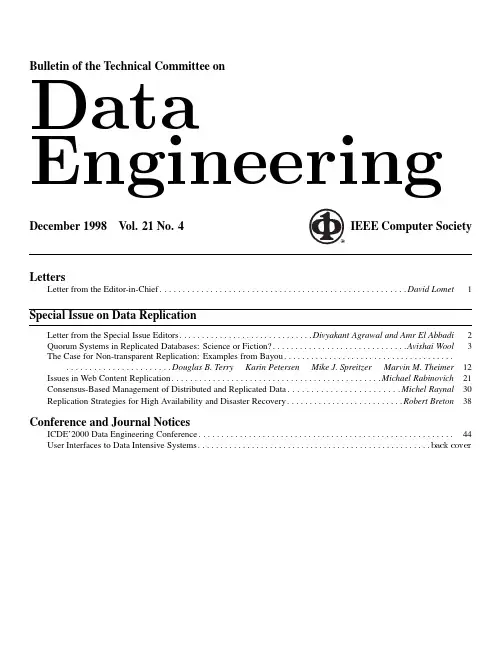
Bulletin of the Technical Committee onDecember1998Vol.21No.4IEEE Computer Society LettersLetter from the Editor-in-Chief......................................................David Lomet1 Special Issue on Data ReplicationLetter from the Special Issue Editors..............................Divyakant Agrawal and Amr El Abbadi2 Quorum Systems in Replicated Databases:Science or Fiction?..............................Avishai Wool3 The Case for Non-transparent Replication:Examples from Bayou.............................................................Douglas B.Terry Karin Petersen Mike J.Spreitzer Marvin M.Theimer12 Issues in Web Content Replication..............................................Michael Rabinovich21 Consensus-Based Management of Distributed and Replicated Data........................Michel Raynal30 Replication Strategies for High Availability and Disaster Recovery..........................Robert Breton38 Conference and Journal NoticesICDE’2000Data Engineering Conference (44)User Interfaces to Data Intensive Systems....................................................Editorial BoardEditor-in-ChiefDavid B.LometMicrosoft ResearchOne Microsoft Way,Bldg.9Redmond WA98052-6399lomet@Associate EditorsAmr El AbbadiDept.of Computer ScienceUniversity of California,Santa BarbaraSanta Barbara,CA93106-5110Surajit ChaudhuriMicrosoft ResearchOne Microsoft Way,Bldg.9Redmond WA98052-6399Donald KossmannLehrstuhl f¨u r Dialogorientierte SystemeUniversit¨a t PassauD-94030Passau,GermanyElke RundensteinerComputer Science DepartmentWorcester Polytechnic Institute100Institute RoadWorcester,MA01609The Bulletin of the Technical Committee on Data Engi-neering is published quarterly and is distributed to all TC members.Its scope includes the design,implementation, modelling,theory and application of database systems and their technology.Letters,conference information,and news should be sent to the Editor-in-Chief.Papers for each issue are so-licited by and should be sent to the Associate Editor re-sponsible for the issue.Opinions expressed in contributions are those of the au-thors and do not necessarily reflect the positions of the TC on Data Engineering,the IEEE Computer Society,or the authors’organizations.Membership in the TC on Data Engineering(http: www.is open to all current members of the IEEE Com-puter Society who are interested in database systems. The web page for the Data Engineering Bulletin is /research/db/debull. The web page for the TC on Data Engineering is /groups/IEEE/tcde/index.html.TC Executive Committee ChairBetty SalzbergCollege of Computer ScienceNortheastern UniversityBoston,MA02115salzberg@ Vice-ChairErich J.NeuholdDirector,GMD-IPSIDolivostrasse15P.O.Box1043266100Darmstadt,Germany Secretry/TreasurerPaul LarsonMicrosoft ResearchOne Microsoft Way,Bldg.9Redmond WA98052-6399 SIGMOD LiasonZ.Meral OzsoyogluComputer Eng.and Science Dept.Case Western Reserve UniversityCleveland,Ohio,44106-7071 Geographic Co-ordinatorsMasaru Kitsuregawa(Asia)Institute of Industrial ScienceThe University of Tokyo7-22-1Roppongi Minato-kuTokyo106,JapanRon Sacks-Davis(Australia)CITRI723Swanston StreetCarlton,Victoria,Australia3053Svein-Olaf Hvasshovd(Europe)ClustRaWestermannsveita2,N-7011Trondheim,NORWAY DistributionIEEE Computer Society1730Massachusetts AvenueWashington,D.C.20036-1992(202)371-1013twoods@Letter from the Editor-in-ChiefOur New Financial Plan–For the Last TimeThe TC on Data Engineering does not generate enough revenue to adequately fund the Bulletin.As TC Chair Betty Salzberg explained it in the June issue,“we will no longer be automatically mailing out paper copies of the Bulletin to all members of the TC.This will cut down on the expenses of the TC without,we hope,causing undue inconvenience to our members,most of whom will get their copies of the Bulletin through the Bulletin web page.”This information is included in the Bulletin,as hardcopy distribution is our only sure way to reach all TC members.If you are unable to access the Bulletin via our web site and want to continue receiving it,you must contact Tracy Woods,IEEE Computer Society,1730Massachusetts Ave.,Washington,DC20036now.This issue is the last issue that will be sent in hardcopy to all members.The Bulletin and the SIGMOD AnthologyAs most of you undoubtedly know,ACM SIGMOD has undertaken to produce an Anthology CDRom containing the complete set of SIGMOD and PODS conference proceedings.The Anthology is being edited by Michael Ley, who has produced a preliminary version for the SIGMOD and DBLP web sites.These sites index all the articles to be included in the anthology.The index plus full articles will appear on the Anthology CD.The anthology is an initiative of SIGMOD chair Rick Snodgrass,who envisioned a portable,fully-searchable, electronic repository of all relevant database conferences and publications.Currently,the Anthology is slated to include the SIGMOD,PODS,and VLDB proceedings and SIGMOD Record.In addition,the TC on Data Engineering was happy to agree to have the Bulletin(1993-1998)also included.So,even when you are not“on-line”,there is no reason to be without full access to these issues of the Bulletin-and of course,to the database material from the ACM and VLDB.I regard the Anthology project as an incredible plus for our community,and applaud the efforts of Rick and Michael in making it a reality.It has been a real pleasure to participate in this collaborative effort of ACM SIGMOD,VLDB and IEEE TCDE and to see the Bulletin included in the anthology.You can get an early look at the anthology by visiting the SIGMOD web site for it at/sigmod/dblp/db/anthology.html.This IssueDatabase replication has become an increasing exploited technology.It is an important technique for ensur-ing high availability,and plays an important role in performance of distributed database mercial database vendors have supported replication for a number of years.Sybase was one of the earliest in this market, and the issue contains an article describing its approach.But replication is by no means a”done deal”.It is still an area of active research.These include exploiting replication on the web and using it to improve distributed sys-tems algorithms.And then there is the perennial topic of managing replicas,of how rapidly to propagate changes to replicated data,and how to sort out which replicas need to be read and/or written.I want to thank Amr El Ab-badi and Divy Agrawal,who jointly edited the issue,and the authors for producing this interesting and timely issue containing articles addressing these subjects.David LometMicrosoft Research1Letter from the Special Issue EditorsData replication is one of the oldest and most persistent topics of research in distributed databases.It holds the promise of solving both problems of fault-tolerance and performance.By replicating the data on remote sites, failures may occur and users may still be able to access data;alternatively,if a data item is replicated on a localor nearby site,accesses to that copy are efficient and may involve very low overhead.To obtain these benefits, however,complex and expensive synchronization mechanisms are often needed to maintain the consistency and integrity of data.In fact it has often been argued that due to the synchronization overheads and the increased possibility of deadlock,replication is impractical.Nevertheless,the appeal of replication persists and sometimes even migrates to commercial industrial products.In this special issue various researchers and practitioners will address the current state of replication and its promises.Thefirst paper,written by Avishai Wool,addresses head-on the promise of replication and asks the question:Is it science orfiction?He explores this question in the context of quorum-based replication and discusses its potential to solve the problems of managing replicated databases.Avishai explains why quorum systems have not fulfilled their old promises,but at the same time argues why new technological advances and applications have brought new requirements that can be addressed by quorums.In fact,he shows that quorum systems may offer a way to scale up throughput in heavily loaded systems.Many replicated storage systems have advocated relaxed consistency models to get improved availability, scalability and performance.Doug Terry,Karin Petersen,Mike Spreitzer and Marvin Theimer discuss the case for non-transparent replication using the Bayou system.The Bayou system developed at Xerox PARC is an exampleof a replicated storage system that was designed to strike a balance between application control and complexity.In this paper the authors discuss the tension between overburdening and underpowering applications.They discuss two bayou applications,a calendar manager and a mail reader,and illustrate ways in which they utilize Bayou’s features to manage their data in an application-specific manner.The web is a natural context for replication with its increasing scalability and performance demands.Micha Rabinovich examines various issues that arise in Web content replication,paying special attention to challengesin dynamic replication.The paper starts with an overview of the current state of replication and caching on the web.It then proceeds to offer valuable insights into open questions and research issues both from architecturalas well as from algorithmic points of view.In the next paper,Michel Raynal addresses the problem of atomic commitment in distributed replicated databases. He shows that solutions to the consensus problem can be very useful in developing solutions to the atomic com-mitment problem.In particular,he develops a solid theoretical foundation for identifying the minimal assump-tions a system must satisfy in order to develop non-blocking replica control protocols in spite of process crashes and asynchrony.Finally,Bob Breton presents the evolution of a replication system,Sybase’s Replication Server,and discusses how it supports disaster recovery as well as support for high availability business requirements.In particular,he discusses the need for replication as a means for disaster recovery in real applications that have very stringent availability requirements.In the paper he also discusses a number of alternatives for high availability database architectures and outlines the main risks and benefits of each approach.Divyakant Agrawal and Amr El AbbadiUC Santa Barbara2Quorum Systems in Replicated Databases:Science or Fiction?Avishai WoolBell Labs,Lucent Technologies,Murray Hill,New Jersey,USAE-mail:yash@/˜yash/AbstractA quorum system is a collection of subsets of servers,every two of which intersect.Quorum systemshave been suggested as a tool for concurrency control in replicated databases almost twenty years ago.They promised to guarantee strict consistency and to provide high availability and fault-tolerance in the face of server crashes and network partitions.Despite these promises,current commercial replicated databases typically do not use quorum systems.Instead they use mechanisms which guarantee much weaker consistency,if any.Moreover,the interest in quorum systems seems to be waning even in the database research community.This paper attempts to explain why quorum systems have not fulfilled their old promises,and at the same time to argue why the current state of affairs may change.As technological advances bring new capabilities,and new applications bring new requirements,the time may have come to review the validity of some long standing criticisms of quorum systems.Another theme of this paper is to argue that if quorum systems are to play a role in database research, it is not likely to be for their claimed fault-tolerance capabilities.Rather,more attention should be given to a somewhat overlooked feature of quorum systems:they allow load balancing among servers while maintaining strict consistency.Thus quorum systems may offer a way to scale up the throughput of heavily loaded servers.1IntroductionA quorum system is a collection of subsets(quorums)of servers,every two of which intersect.During the late 70’s and early80’s,quorum systems were proposed as a basic mechanism for concurrency control in replicated databases[Tho79,Gif79,GB85,Mae85,Her86].Informally,a quorum-based replication scheme works as fol-lows.Data items are timestamped and written to some quorum of servers.In order to read a data item,the reader accesses the copies held by a(possibly different)quorum of servers,and uses the value with the highest times-tamp.The quorum intersection property guarantees that at least one server observes both operations,so the reader Copyright1998IEEE.Personal use of this material is permitted.However,permission to reprint/republish this material for ad-vertising or promotional purposes or for creating new collective works for resale or redistribution to servers or lists,or to reuse any copyrighted component of this work in other works must be obtained from the IEEE.Bulletin of the IEEE Computer Society Technical Committee on Data Engineering3in fact obtains the most up-to-date value.It is easy to see that this approach,coupled with standard two-phase protocols,ensures that strict consistency can be maintained and that the transactions can be globally serialized.Quorum systems were attractive to database researchers mainly because they offer a de-centralized approach that tolerates failures.For instance,quorum-based databases are able to maintain their consistency even in the presence of network partitions[DGS85]and server crashes(as quantified by their fault-tolerance[BG86]).How-ever,the quorum approach’s promise of high availability was arguably its most desirable feature,and it certainly generated a substantial amount of research(e.g.,[BG87,ET89,PW95,AW98]).Availability is the probability that the member servers of at least one quorum are functioning,assuming that the servers crash independently with afixed probability,and that the complete database is replicated at every server.Many quorum systems,such as those of[KC91,Kum91,AE91,RST92,PW97b,PW97a,Baz96],exhibit very high availability,and moreover, their availability tends to1very rapidly as the system scales up and more servers are added.Despite these features,quorum systems are not in wide-spread use within commercial replicated databases. As an example,we can consider the Oracle8product[Ora97],which provides several modes of data replication. Among these,the only mode that guarantees serializability,called Synchronized Data Propagation,uses a Read-One-Write-All(ROWA)approach(cf.[HHB96]).Oracle’s product documentation in fact recommends not to use this mode because“it can function only when all sites in the system are concurrently available”[Ora97, p.30–26],i.e.,it has very poor write-availability.All the other modes of replication supported by Oracle8es-sentially take a lazy replication,primary-copy approach,coupled with various heuristics which attempt to detect and resolve some common conflict scenarios.It is well known that such schemes do not guarantee serializability, and in fact serializability can only be guaranteed if the data placement graph is acyclic[CRR96].There are some valid reasons why quorum systems have not yet been used in replicated databases.In the next section we shall list the more common criticisms,and discuss whether they are still valid today.Then in Section3 we contrast the situation in the database world with other domains where quorum systems have been successfully deployed.In Section4we suggest that by shifting the focus from fault-tolerance to improved performance,we can realize that the load-balancing capability of quorum systems has significant,yet overlooked,potential.We also briefly touch upon some new applications that may benefit from a quorum-based replicated database,and we conclude with Section5.2Common Arguments Against Quorum Systems2.1The Local Read ParadigmOne of the most common arguments against quorum systems is that they require accessing one or more remote copies for read operations,and that incurring a network delay for reads is prohibitively expensive.If this view is adopted,we reach the local read paradigm:read operations are only allowed to access items that are stored on the local machine.An immediate consequence is that variants of ROWA become the only allowable replication schemes,and in particular quorum-based replication is excluded.However,technological advances are working against this argument,since data networks are improving faster than disks are.For instance,the bandwidth available on local area networks(LANs)has improved from around 10Mbps to around1Gbps—a100fold increase—over the last decade,whereas disk transfer rates only improved from about1Mbps to10Mbps over the same period.As for latency,network latency is mostly due to protocol software which improves with CPU speed,whereas disk latency is limited by the mechanics of the seek time and the disk rotation speed[GR93,pp.53,59].In the setting of LANs there should be little doubt that the local read paradigm is no longer justified.In fact, a“local”read often includes a LAN access anyway,since the client software usually runs on a separate machine rather than directly on the DB server machine.Moreover,LANs typically have hardware-based broadcast com-munication primitives,so sending a read request(such as a high level SQL command)to a quorum of servers can be achieved by a single message.The multiple reads all execute in parallel,thus the reader would not even4suffer a substantially longer delay.To some extent,remote reads over a LAN may be reasonable even for main memory databases[GS92,JLR94],or if the data is held in the cache;the incurred networking delay would be more than that of a pure memory access,but still much less than a disk access.Current wide area networks(WANs)are still somewhat slower than LANs(e.g.,155Mbps for an OC3line), and the latency in a WAN depends on the geographical distance and on the number of routers between the end-points.Nevertheless the argument that networks improve faster than disks still holds.This is especially true in a private network or a virtual private network(VPN),where quality of service can be guaranteed.So the validity of the local read paradigm is becoming more questionable in the wide-area setting too.There is some evidence that at least the database research community may be moving away from the local read paradigm.Over the last two years we have seen the emergence of several replication schemes in the database literature,schemes which do not adhere to the local read paradigm quite so strictly.For instance,the protocol of [GHOS96]includes obtaining locks from remote machines even for read-only transactions,and the protocols of[BK97]include obtaining read,write,and commit permissions from a replication-graph-manager machine. These protocols have yet to be implemented in an actual database,but simulations of their performance over WANs[ABKW98]show that the network is not a bottleneck for either protocol.We can conclude that while the local read paradigm was a valid objection to quorum-based replication for many years,its validity is diminishing with time.Remote reads should no longer be considered to be prohibitivea priori.In many settings they are quite reasonable.2.2Reads vs.WritesAnother criticism of quorum systems is that when read operations are much more frequent than write operations, which is a typical scenario,optimizing the read operations is more important than optimizing the writes[GR93]. In such scenarios the total amount of work incurred by a ROWA approach is claimed to be lower than that of a quorum-based approach(where total work is measured by the total number of disk accesses or total number of messages per operation).Since this is a quantitative issue,we can perform the following back-of-the-envelope calculation.Assume a system of machines,in which writes comprise an fraction of the submitted operations and reads comprise the other fraction.Then on average a quorum-based approach with read quorums of machines and write quorums of machines would incur a total work of(1) per operation.In comparison,a ROWA approach,whether lazy or not,would incur a total work of(2) Simple manipulations yield that when(3) and if we assume further that read and write quorums have equal size we end with the condition(4) So we see that one approach is not universally better than the other.The choice depends not only on the frequency of write operations,but also on the ratio of read quorum size to number of replicas.For instance,using Maekawa’s quorum system[Mae85],if and,a quorum-based approach incurs less work than ROWA when33%of the operations are writes.If and then the crossover5point is25%writes.In general,for this system,so the frequency of writes needs only to exceed for the quorum-based approach to be advantageous.Quorum systems with variable-sized quorums,such as those of[AE91,PW97a],offer the possibility of outperforming ROWA for even lower write rates,by directing reads to smaller sized quorums,which can be as small as for both systems.Clearly,as the number of replicas grows,quorum systems become advantageous for lower write rates.But even for reasonably small systems and moderate write rates,formula(4)shows that quorum-based systems may outperform ROWA-based ones according to the total work measure.2.3A Reality Check on AvailabilityThe promise of high availability has been an important part in the development of the theory of quorum systems. However in practice this promise seems not to have materialized as predicted by the theory.The reason is that several seemingly benign modeling assumptions are made in order to make the analysis of availability tractable. Unfortunately,these assumptions clash with the reality of network environments in crucial ways.The standard probabilistic assumptions which underly the definition of availability,as analyzed in[BG87,PW95]and others, are:1.Crashes are independent events.2.The communication network is fully connected and never fails.3.All the servers have the same crash probability.Under these assumptions,the availability of a quorum system is the probability of the event that there exists some quorum for which all the servers are functioning.Note that assumption2does not in itself conflict with the fact that quorum systems guarantee strict consis-tency despite partitions[DGS85].One may hope that assuming perfect communication,for the purpose of avail-ability analysis,would not change the qualitative predictions of the model.As we shall see,though,this modeling is problematic.Assumption3(uniform crash probability)simplifies the analysis but is not really crucial.It was shown by [SB94,AW98]that essentially the same properties hold with or without it,namely that the optimal availability quorum system is defined by weighted voting,where the optimal weights depend on the individual crash proba-bilities.If all the servers have the same crash probability this voting system reduces to either a simple majority voting,which has optimal availability when[BG87],or to a monarchy(single server)when[PW95].Assumptions1and2are not so easily dealt with,as seen from the experiments of[AW96].These experiments measured crashes and network connectivity over a period of6months,on a system that consisted of14machines on3LANs,split between two geographical locations50km apart,using Internet(UDP)communications.The experiments measured application-level“crashes”:Whenever the measuring daemon on some machine could not function,for whatever reason,a crash was counted.These experiments show that within a LAN,it is quite reasonable to assume that the communication is perfect—but the crash independence assumption is misleading.Crashes of machines on a LAN were found to be positively correlated,which is explained by a dependence on commonfile systems,domain name servers(DNS),adminis-trative staff,power supply,and so forth.Such a positive crash correlation has a dramatic effect on the availability: In the extreme case,if all the machines crash and revive at identical times,any quorum system will have precisely the same availability as that of a single server.In fact[AW96]observe that the most highly available machine on one of the LANs was down1.25%of the time,yet using a majority-based quorum system with this machine and5others on the same LAN only reduced the unavailability to1.12%.This is a far smaller boost than that predicted under the independent crashes assumption.6As for WANs,the reverse situation occurs.The experiments of[AW96]show that crash independence be-tween geographically distant sites is a valid assumption—but that the perfect communication assumption is not. The experimental system was partitioned into two or more disconnected components during6.5%of the time. Thus the portion of the Internet that took part in the study is better modeled by a tree of fully-connected clusters, where each cluster corresponds to a LAN.In such a non-fully-connected network model,it is known that the optimal-availability quorum system is completely contained in a single bi-connected component[INK95].And indeed the experiments of[AW96]showed that confining the quorum system to6machines on a single LAN gave better availability than using all14machines and allowing quorums to span the two sites.Thus the shortcomings of the crash independence and perfect communication assumptions form a double-edged sword,which severely limits the predictive power of the standard availability model.On one hand,if all the replicas are placed on a single LAN,crash correlations cancel most of the availability boosting that quorum systems claim to have.On the other hand,if the replicas are placed in geographically distant sites,network par-titions have an even more damaging effect.There are several ways to avoid these problems,but they are typically unpleasant.Crash correlation on a LAN can be decreased by duplicating and separating all the common resources,such asfile systems,DNS,power supply,etc.,which is costly and hard to work partitions are very hard to control over the public Internet,since currently nothing can be guaranteed in terms of quality of service.Therefore a high-availability wide area system would probably need to operate its own private high-connectivity network—again an expensive prospect.The latter approach is the one taken by some successful systems(see Section3),but it is hardly within every organization’s budget.The conclusion we can draw here is somewhat sobering.If quorum systems are to play a significant role in the future of replicated databases,it will not be because they offer high availability,but for some other reason.In Section4we shall see one possible such reason,which is the capability of quorum systems to support extremely high load,in a scalable way,without weakening the database’s consistency.3Some Success Stories3.1V AX Clusters and Financial ApplicationsQuorum systems are used deep within thefile system of Digital’s OpenVMS operating system,as a basic com-ponent of the V AX Cluster technology[VMS].A V AX Cluster of machines will function as long as a quorum (majority)of the machines are alive and able to communicate with each other.If the live machines in the cluster do not constitute a connected quorum,they will freeze all activity and wait for a quorum to be re-established. This assures that a cluster that has been partitioned will not allow access to the same data from multiple,discon-nected machines,since at most one component of a partition(one that still has a quorum)can write to the data. This guarantees proper access tofiles across the entire distributedfile system.The communication networks that are typically used in V AX Cluster systems are either LANs,or FDDI-based metropolitan-wide networks,running the DECnet communication protocols.Fairly large cluster configurations, comprising dozens of servers(the limit is96machines),are in actual use.This technology is especially attractive tofinancial applications,for the following reasons:(i)strict data con-sistency is crucial;(ii)high reliability is required against disasters such as the1993World Trade Center explosion and thefire at the Credit Lyonnais bank[CL98];and(iii)largefinancial institutions are able to bear the cost of the dedicated communication networks.Note that the V AX Cluster’s quorum system does not provide a quorum-based replicated database per se.The system supportsfile-system semantics but does not provide transaction processing.And in fact the rdb database product,which is now owned by Oracle but originated on Digital’s VMS systems[RDB98],uses the V AX Clus-ter’s lock manager but does not use a quorum-based replication scheme.7。